 | –≠–ª–µ–∫—Ç—Ä–æ–Ω–Ω—ã–π –∫–æ–º–ø–æ–Ω–µ–Ω—Ç: MAX4289 | –°–∫–∞—á–∞—Ç—å:  PDF PDF  ZIP ZIP |

General Description
The MAX4289 micropower, operational amplifier is opti-
mized for ultra-low supply voltage operation. The ampli-
fier consumes only 9µA of quiescent supply current and
is fully specified for operation from a single 1.0V to 5.5V
power supply. This ultra-low voltage operation together
with the low quiescent current consumption make the
MAX4289 ideal for use in battery-powered systems
operated from as little as a single alkaline cell. The
MAX4289 also features a wide input common-mode
range that includes the ground, and an output voltage
swing that is virtually Rail-to-Rail
Æ
, allowing almost all of
the power supply to be used for signal voltage.
The low input offset voltage and low input bias current
specifications along with the high open-loop gain make
the MAX4289 well-suited to applications requiring a
high degree of precision.
The MAX4289 is available in a tiny 6-pin SOT23 pack-
age. All specifications are guaranteed over the extend-
ed temperature range of -40∞C to +85∞C.
Applications
Features
o Ultra-Low Voltage Operation: Guaranteed
Specifications from 1.0V to 5.5V
o Input Common-Mode Range: 0 to (V
CC
- 0.2V)
o Ultra-Low Power Consumption: 9µA Supply
Current (typ)
o Optimized for Operation from Single-Cell
Battery-Powered Systems
o Compatible with 3.0V and 5.0V Single-Supply
Systems
o Low Offset Voltage: 0.2mV
o Low Input Bias Current: 5nA
o High Open-Loop Voltage Gain: 90dB
o Rail-to-Rail Output Stage Drives 5k Load
o No Output Phase Reversal for Overdriven Inputs
o Available in a Tiny 6-Pin SOT23 (3mm
3mm)
MAX4289
1.0V Micropower, SOT23, Operational Amplifier
________________________________________________________________ Maxim Integrated Products
1
GND
IN-
IN+
1
6
V
CC
OUT
MAX4289
SOT23-6
TOP VIEW
2
3
4
OUT
N.C.
GND
1
2
8
7
N.C.
V
CC
IN-
IN+
N.C.
SO-8
3
4
6
5
MAX4289
5
N.C.
Pin Configurations
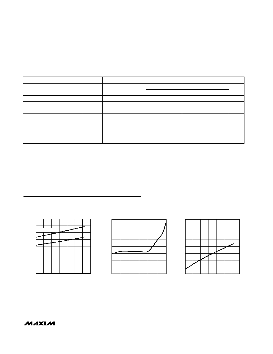
Typical Operating Characteristic
Ordering Information
19-2023; Rev 0; 1/02
For pricing, delivery, and ordering information, please contact Maxim/Dallas Direct! at
1-888-629-4642, or visit Maxim's website at www.maxim-ic.com.
PART
TEMP RANGE
PIN-
PACKAGE
TOP
MARK
MAX4289EUT-T
-40∞C to +85∞C
6 SOT23-6
AARX
MAX4289ESA
-40∞C to +85∞C
8 SO
--
50
60
70
80
90
POWER-SUPPLY REJECTION RATIO
vs. SUPPLY VOLTAGE
SUPPLY VOLTAGE (V)
PSRR (dB)
0.8
1.1
1.2
0.9
1.0
1.3
1.4
1.5
T
A
= +85
∞C
T
A
= +25
∞C
T
A
= -40
∞C
Single-Cell Systems
Portable Electronic
Equipment
Battery-Powered
Instrumentation
Hearing Aids Using Zinc
Air Battery
Strain Gauges
Cellular Phones
Notebook Computers
Sensor Amplifiers
Portable Communication
Devices
Rail-to-Rail is a registered trademark of Nippon Motorola, Ltd.

MAX4289
1.0V Micropower, SOT23, Operational Amplifier
2
_______________________________________________________________________________________
ABSOLUTE MAXIMUM RATINGS
ELECTRICAL CHARACTERISTICS
(V
CC
= 3V, V
CM
= 0, V
OUT
= V
CC
/2, R
L
tied to V
CC
/2, T
A
= T
MIN
to T
MAX
, unless otherwise noted. Typical values are at T
A
= +25∞C.)
(Note 1)
Stresses beyond those listed under "Absolute Maximum Ratings" may cause permanent damage to the device. These are stress ratings only, and functional
operation of the device at these or any other conditions beyond those indicated in the operational sections of the specifications is not implied. Exposure to
absolute maximum rating conditions for extended periods may affect device reliability.
Power-Supply Voltage (V
CC
to GND).......................................6V
Input Voltage (IN+ or IN-) ...........................(V
CC
+ 0.3V) to -0.3V
Input Current (IN+ or IN-)....................................................20mA
Output Short-Circuit Duration to V
CC
or GND ............Continuous
Continuous Power Dissipation (T
A
= +70∞C)
6-Pin SOT23 (derate 8.7mW/∞C above +70∞C).............696mW
8-Pin SO (derate 5.88mW/∞C above +70∞C).................471mW
Operating Temperature Range ...........................-40∞C to +85∞C
Junction Temperature ......................................................+150∞C
Storage Temperature Range .............................-65∞C to +150∞C
Lead Temperature (soldering, 10s) .................................+300∞C
PARAMETER
SYMBOL
CONDITIONS
MIN
TYP
MAX
UNITS
T
A
= +25∞C
1.0
5.5
Supply Voltage Range
V
CC
Inferred from the
PSRR tests
T
A
= -40∞C to +85∞C
1.2
5.5
V
V
CC
= 1.0V, T
A
= +25∞C
9
14
V
CC
= 3.0V
12
25
Quiescent Supply Current
I
CC
V
CC
= 5.5V
18
40
µA
T
A
= +25∞C
±0.2
±2.0
Input Offset Voltage
V
OS
T
A
= T
MIN
to T
MAX
±6.0
mV
Input Bias Current
I
B
±5
±15
nA
Input Offset Current
I
OS
±0.5
±2.0
nA
Differential Input Resistance
R
IN
50
M
V
CC
= 1.2V
0
V
CC
- 0.2
Input Common-Mode Voltage
Range
V
CM
Inferred from
CMRR test
V
CC
= 3.0V
0
V
CC
- 0.8
V
V
CC
= 1.2V, 0
V
CC
- 0.2V
57
V
CC
= 1.2V, 0
V
CM
V
CC
- 0.8V
57
85
Common-Mode Rejection Ratio
CMRR
V
CC
= 3.0V, 0
V
CM
V
CC
- 0.8V
57
110
dB
1.0V
V
CC
5.5V, T
A
= +25∞C
54
75
Power-Supply Rejection Ratio
PSRR
1.2V
V
CC
5.5V, T
A
= -40∞C to +85∞C
58
75
dB
R
L
= 100k
(50mV V
OUT
V
CC
- 50mV)
110
Large-Signal Voltage Gain
A
VOL
R
L
= 5k
(100mV V
OUT
V
CC
- 100mV)
80
90
dB
R
L
= 100k
0.2
10
Output Voltage Swing High
V
OH
Specified as
|V
CC
- V
OH
|
R
L
= 5k
7
40
mV
R
L
= 100k
0.4
10
Output Voltage Swing Low
V
OL
Specified as V
OL
R
L
= 5k
7
40
mV
MAX4289
1.0V Micropower, SOT23, Operational Amplifier
_______________________________________________________________________________________
3
ELECTRICAL CHARACTERISTICS (continued)
(V
CC
= 3V, V
CM
= 0, V
OUT
= V
CC
/2, R
L
tied to V
CC
/2, T
A
= T
MIN
to T
MAX
, unless otherwise noted. Typical values are at T
A
= +25∞C.)
(Note 1)
PARAMETER
SYMBOL
CONDITIONS
MIN
TYP
MAX
UNITS
V
CC
= 1.0V
0.6
Output Short-Circuit Current
I
OUT
Sourcing/sinking
current
V
CC
= 3.0V
19
mA
Power-Up Time
t
PU
300
µs
Input Capacitance
C
IN
3.0
pF
Gain-Bandwidth Product
GBW
17
kHz
Phase Margin
M
80
d egr ees
Gain Margin
GM
10
dB
Slew Rate
SR
6
V/ms
Capacitive-Load Stability
A
VCL
= +1V/V, no sustained oscillations
200
pF
Settling Time to 0.1%
t
S
A
VCL
= +1V/V, no sustained oscillations
75
µs
Note 1: All specifications are 100% production tested at T
A
= +25∞C. Temperature specification limits are guaranteed by design.
Typical Operating Characteristics
(V
CC
= 3V, V
CM
= 0, R
L
to V
CC
/2, T
A
= +25∞C, unless otherwise noted.)
SUPPLY CURRENT vs. TEMPERATURE
MAX4289 toc01
0
2
6
4
12
14
10
8
16
SUPPLY CURRENT (
µ
A)
-40
0
20
-20
40
60
80
100
TEMPERATURE (
∞C)
V
CC
= 3V
V
CC
= 1V
-0.8
-0.6
-0.4
-0.2
0
0.2
0.4
0.6
0.8
0
1.0
0.5
1.5
2.0
2.5
3.0
INPUT OFFSET VOLTAGE
vs. INPUT COMMON-MODE VOLTAGE
MAX4289 toc02
INPUT COMMON-MODE VOLTAGE (V)
INPUT OFFSET VOLTAGE (mV)
INPUT OFFSET VOLTAGE
vs. TEMPERATURE
MAX4289 toc03
-0.8
-0.6
-0.2
-0.4
0.4
0.6
0.2
0
0.8
INPUT OFFSET VOLTAGE (mV)
-40
0
20
-20
40
60
80
100
TEMPERATURE (
∞C)

MAX4289
1.0V Micropower, SOT23, Operational Amplifier
4
_______________________________________________________________________________________
Typical Operating Characteristics (continued)
(V
CC
= 3V, V
CM
= 0, R
L
to V
CC
/2, T
A
= +25∞C, unless otherwise noted.)
4
6
5
8
7
9
10
-40
20
40
-20
0
60
80
100
INPUT BIAS CURENT
vs. TEMPERATURE
MAX4289 toc04
TEMPERATURE (
∞C)
INPUT BIAS CURRENT (nA)
30
20
10
0
-10
0
1.5
0.5
1.0
2.0
2.5
3.0
INPUT BIAS CURRENT
vs. INPUT COMMON-MODE VOLTAGE
MAX4289 toc05
INPUT COMMON-MODE VOLTAGE (V)
INPUT BIAS CURRENT (nA)
0
6
4
2
10
8
18
16
14
12
20
-40
-20
0
20
40
60
80
100
OUTPUT SWING HIGH
vs. TEMPERATURE
MAX4289 toc06
TEMPERATURE (
∞C)
V
OH
(mV)
R
L
CONNECTED TO GND
R
L
= 5k
R
L
= 100k
0
6
4
2
10
8
18
16
14
12
20
-40
-20
0
20
40
60
80
100
OUTPUT SWING LOW
vs. TEMPERATURE
MAX4289 toc07
TEMPERATURE (
∞C)
V
OL
(mV)
R
L
CONNECTED TO V
CC
R
L
= 5k
R
L
= 100k
30
50
90
70
110
130
0
100
50
150
200
250
300
OPEN-LOOP GAIN
vs. OUTPUT SWING LOW
MAX4289 toc08
V
OUT
FROM GND (mV)
GAIN (dB)
R
L
= 5k
R
L
= 100k
30
50
90
70
110
130
0
100
50
150
200
250
300
OPEN-LOOP GAIN
vs. OUTPUT SWING HIGH
MAX4289 toc09
V
OUT
FROM V
CC
(mV)
GAIN (dB)
R
L
= 5k
R
L
= 100k
60
80
70
100
90
110
120
-40
20
40
-20
0
60
80
100
OPEN-LOOP GAIN vs. TEMPERATURE
MAX4289 toc10
TEMPERATURE (
∞C)
GAIN (dB)
R
L
= 5k
R
L
= 100k
R
L
CONNECTED TO GND
60
80
70
100
90
110
120
-40
20
40
-20
0
60
80
100
OPEN-LOOP GAIN vs. TEMPERATURE
MAX4289 toc11
TEMPERATURE (
∞C)
GAIN (dB)
R
L
= 5k
R
L
= 100k
R
L
CONNECTED TO V
CC
80
-20
0.01
0.1
1
10
100
GAIN AND PHASE vs. FREQUENCY
(C
L
= 0)
0
MAX4289 toc12
FREQUENCY (kHz)
GAIN (dB)
20
40
60
50
30
10
-10
70
180
-20
20
60
100
140
120
80
40
0
160
PHASE (DEGREES)
GAIN
PHASE

MAX4289
1.0V Micropower, SOT23, Operational Amplifier
_______________________________________________________________________________________
5
10
µs/div
SMALL-SIGNAL TRANSIENT RESPONSE
IN
50mV/div
OUT
50mV/div
MAX4289 toc13
200
µs/div
LARGE-SIGNAL TRANSIENT RESPONSE
IN
1V/div
OUT
1V/div
MAX4289 toc14
0.8
0.9
1.0
1.1
1.2
MINIMUM-OPERATING VOLTAGE
vs. TEMPERATURE
MAX4289 toc15
TEMPERATURE (
∞C)
V
CC
(V)
-40
20
40
-20
0
60
80
100
PSRR > 70dB
0
0.3
0.9
0.6
1.2
1.5
0
0.4
0.2
0.6
0.8
1.0
OUTPUT SINKING CURRENT
vs. OUTPUT VOLTAGE
MAX4289 toc16
OUTPUT VOLTAGE (V)
OUTPUT CURRENT (mA)
V
CC
= 1V
SINKING CURRENT
0
5
15
10
20
25
0
1.0
0.5
1.5
2.0
2.5
3.0
OUTPUT SINKING CURRENT
vs. OUTPUT VOLTAGE
MAX4289 toc17
OUTPUT VOLTAGE (V)
OUTPUT CURRENT (mA)
V
CC
= 3V
SINKING CURRENT
0
0.2
0.6
0.4
0.8
1.0
0
0.4
0.2
0.6
0.8
1.0
OUTPUT SOURCING CURRENT
vs. OUTPUT VOLTAGE
MAX4289 toc18
OUTPUT VOLTAGE (V)
OUTPUT CURRENT (mA)
V
CC
= 1V
SOURCING CURRENT
0
5
15
10
20
25
0
1.0
0.5
1.5
2.0
2.5
3.0
OUTPUT SOURCING CURRENT
vs. OUTPUT VOLTAGE
MAX4289 toc19
OUTPUT VOLTAGE (V)
OUTPUT CURRENT (mA)
V
CC
= 3V
SOURCING CURRENT
Typical Operating Characteristics (continued)
(V
CC
= 3V, V
CM
= 0, R
L
to V
CC
/2, T
A
= +25∞C, unless otherwise noted.)