 | ÐлекÑÑоннÑй компоненÑ: MAX4367 | СкаÑаÑÑ:  PDF PDF  ZIP ZIP |
Äîêóìåíòàöèÿ è îïèñàíèÿ www.docs.chipfind.ru
General Description
The MAX4366/MAX4367/MAX4368 are bridged audio
power amplifiers intended for devices with internal
speakers and headsets. The MAX4366/MAX4367/
MAX4368 are capable of delivering 330mW of continu-
ous power into a 32
load, or 200mW into a 16 load
with 1% THD+N from a single 5V supply.
The MAX4366/MAX4367/MAX4368 bridged outputs elimi-
nate the need for output-coupling capacitors minimizing
external component count. The MAX4366/MAX4367/
MAX4368 also feature a low-power shutdown mode,
clickless power-up/power-down and internal DC bias
generation. The MAX4366 is a unity-gain stable, program-
mable gain amplifier. The MAX4367/MAX4368 feature
internally preset gains of 2V/V and 3V/V, respectively.
All devices are available in space-saving 8-pin SOT23,
thin QFN and µMAX packages, and an 8-bump chip-
scale package (UCSPTM).
Applications
Cellular Phones
Two-Way Radios
PDAs
Headphones
Headsets
General-Purpose Audio
Features
o Drives 330mW into 32 (200mW into 16)
o 0.02% THD+N at 1kHz (120mW into 32)
o Internal Bridged Configuration
o No Output-Coupling Capacitors
o 2.3V to 5.5V Single-Supply Operation
o 2mA Supply Current
o Low-Power Shutdown Mode
o Clickless Power-Up and Shutdown
o Thermal Overload Protection
o Available in SOT23, Thin QFN, µMAX, and UCSP
Packages
MAX4366/MAX4367/MAX4368
330mW, Ultra-Small, Audio Power Amplifiers
with Shutdown
________________________________________________________________ Maxim Integrated Products
1
1
2
B
A
C
UCSP
TOP VIEW
(BUMP SIDE
DOWN)
3
BIAS
OUT-
SHDN
IN-
OUT+
IN+
GND
V
CC
MAX4366
MAX4367
MAX4368
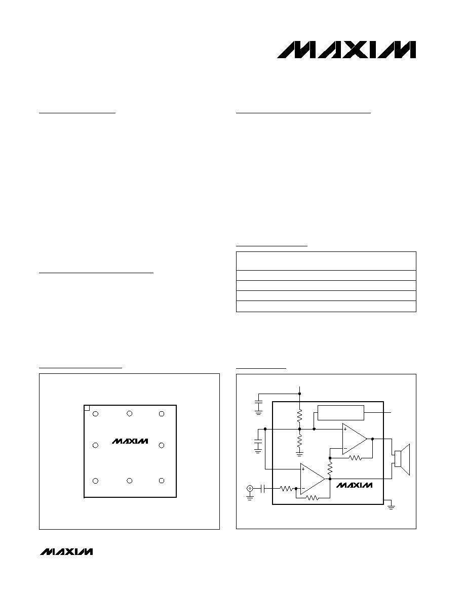
Pin Configurations
Ordering Information
V
CC
V
CC
OUT-
IN-
IN+
BIAS
AUDIO
INPUT
CLICKLESS/POPLESS
SHUTDOWNCONTROL
GND
SHDN
OUT+
MAX4367
MAX4368
Typical Operating Circuit
19-2338; Rev 2; 12/02
For pricing, delivery, and ordering information, please contact Maxim/Dallas Direct! at
1-888-629-4642, or visit Maxim's website at www.maxim-ic.com.
*EP = Exposed paddle.
Ordering Information continued at end of data sheet.
Selector Guide and Functional Diagrams appear at end of
data sheet.
Pin Configurations continued at end of data sheet.
UCSP is a trademark of Maxim Integrated Products, Inc.
PART
TEMP RANGE
PIN/BUMP-
PACKAGE
TOP
MARK
MAX4366EBL-T -40°C to +85°C
8 UCSP-8
AAK
MAX4366EKA-T -40°C to +85°C
8 SOT23-8
AAIO
MAX4366EUA
-40°C to +85°C
8 µMAX
--
MAX4366ETA
-40°C to +85°C
8 Thi n Q FN - E P *
AAC
MAX4366/MAX4367/MAX4368
330mW, Ultra-Small, Audio Power Amplifiers
with Shutdown
2
_______________________________________________________________________________________
ABSOLUTE MAXIMUM RATINGS
ELECTRICAL CHARACTERISTICS
(V
CC
= 5V, R
L
=
, R
IN
= R
F
= 30k
, C
BIAS
= 1µF to GND, SHDN = GND, IN+ = BIAS, T
A
= T
MIN
to T
MAX
, unless otherwise noted.
Typical values are at T
A
= +25°C.) (Note 3)
Stresses beyond those listed under "Absolute Maximum Ratings" may cause permanent damage to the device. These are stress ratings only, and functional
operation of the device at these or any other conditions beyond those indicated in the operational sections of the specifications is not implied. Exposure to
absolute maximum rating conditions for extended periods may affect device reliability.
V
CC
to GND ..............................................................-0.3V to +6V
IN+, IN-, BIAS, SHDN.................................-0.3V to (V
CC
+ 0.3V)
Output Short Circuit to V
CC
or GND (Note 1).............Continuous
Output Short Circuit (OUT+ to OUT-) (Note 1)...........Continuous
Continuous Power Dissipation (T
A
= +70°C)
8-Bump UCSP (derate 4.7mW/°C above +70°C)..........379mW
8-Pin SOT23 (derate 9.7mW/°C above +70°C).............777mW
8-Pin µMAX (derate 4.5mW/°C above +70°C) ..............362mW
8-Pin Thin QFN (derate 24.4mW°C above +70°C) .....1951mW
Operating Temperature Range ...........................-40°C to +85°C
Junction Temperature ......................................................+150°C
Storage Temperature Range .............................-65°C to +150°C
Lead Temperature (soldering, 10s) .................................+300°C
Bump Temperature (soldering) (Note 2)
Infrared (15s) ................................................................+220°C
Vapor Phase (60s) ........................................................+215°C
PARAMETER
SYMBOL
CONDITIONS
MIN
TYP
MAX
UNITS
Supply Voltage Range
V
CC
Inferred from PSRR test
2.3
5.5
V
Supply Current
I
CC
(Note 4)
2
4.3
mA
Shutdown Supply Current
I
SHDN
SHDN = V
CC
35
100
µA
V
IH
1.8
SHDN Threshold
V
IL
0.8
V
SHDN Input Bias Current
-400
nA
Common-Mode Bias Voltage
V
BIAS
(Note 5)
V
CC
/2
- 5%
V
CC
/2
V
CC
/2
+ 5%
V
MAX4366, R
IN
=
±5
±15
MAX4367, IN- = open
±5
±15
Output Offset Voltage
V
OS
MAX4368, IN- = open
±5
±7.5
±15
mV
MAX4366 (open loop)
100
dB
MAX4367 (internally set)
2
Differential Voltage Gain
A
V
(Note 6)
MAX4368 (internally set)
3
V/V
Input Common-Mode Range
V
CM
0.3
V
CC
-
1.0
V
Differential Input Resistance
R
IN(DIFF)
MAX4366, V
IN+
- V
IN-
= 10mV
500
k
Input Resistance
V
IN
- = 0V to V
CC
(MAX4367/MAX4368)
20
k
T
A
= +25°C
70
80
Power-Supply Rejection Ratio
PSRR
V
CC
= 2.3V to
5.5V
T
A
= T
MIN
to T
MAX
66
dB
Common-Mode Rejection Ratio
CMRR
0V
V
CM
V
CC
- 1.0V (MAX4366)
80
dB
2.7V
V
CC
5.5V,
0.6V
V
OUT
V
CC
- 0.6V
±87
±125
Output Source/Sink Current
I
OUT
(Note 7)
2.3V
V
CC
2.7V,
0.6V
V
OUT
V
CC
- 0.6V
±115
mA
R
L
= 16
60
200
Output Power
P
O
f = 1kHz,
THD+N <1%
(Note 8)
R
L
= 32
120
330
mW
MAX4366/MAX4367/MAX4368
330mW, Ultra-Small, Audio Power Amplifiers
with Shutdown
_______________________________________________________________________________________
3
ELECTRICAL CHARACTERISTICS (continued)
(V
CC
= 5V, R
L
=
, R
IN
= R
F
= 30k
, C
BIAS
= 1µF to GND, SHDN = GND, IN+ = BIAS, T
A
= T
MIN
to T
MAX
, unless otherwise noted.
Typical values are at T
A
= +25°C.) (Note 3)
PARAMETER
SYMBOL
CONDITIONS
MIN
TYP
MAX
UNITS
P
O
= 60mW, R
L
= 16
0.04
Total Harmonic Distortion Plus
Noise
THD+N
A
V
= - 2V /V , f = 1kH z
( M AX 4366)
(Notes 9 and 10)
P
O
= 120mW, R
L
= 32
0.02
0.15
%
Noise
f = 10kHz, referred to input
20
nV/
Hz
To V
CC
185
Short-Circuit Current
I
SC
To GND
215
mA
Thermal Shutdown Threshold
165
°C
Thermal Shutdown Hysteresis
10
°C
Power-Up Time
t
PU
60
ms
Shutdown Time
t
SHDN
20
ms
Enable Time from Shutdown
t
ENABLE
60
ms
Note 1: Continuous power dissipation must also be observed.
Note 2: This device is constructed using a unique set of packaging techniques that impose a limit on the thermal profile the device
can be exposed to during board-level solder attach and rework. This limit permits only the use of the solder profiles recom-
mended in the industry-standard specification, JEDEC 020A, paragraph 7.6, Table 3 for IR/VPR and convection reflow.
Preheating is required. Hand or wave soldering is not allowed.
Note 3: All specifications are 100% tested at T
A
= +25°C; temperature limits are guaranteed by design.
Note 4: Quiescent power-supply current is specified and tested with no load on the outputs. Quiescent power-supply current
depends on the offset voltage when a practical load is connected to the amplifier.
Note 5: Common-mode bias voltage is the voltage on BIAS and is nominally V
CC
/2.
Note 6: Differential voltage gain for the MAX4366 is specified as an open-loop parameter because external resistors are used to set
the closed-loop gain. The MAX4367/MAX4368 contain internal feedback resistors that preset the differential voltage gain.
Differential voltage gain is defined as (V
OUT+
- V
OUT-
) / (V
IN
- V
BIAS
). All gains are specified over an output voltage range of
0.6V
V
OUT
4.4V.
Note 7: Specification applies to either output. An amplifier peak output current of 87mA is required to support an output load power
of 60mW for a 16
load, or 120mW for a 32 load.
Note 8: Output power specifications are inferred from the output current test. For 60mW into a 16
load, I
OUT(PEAK)
is 87mA and
V
OUT(P-P)
is 1.39V per amplifier. For 120mW into a 32
load, I
OUT(PEAK)
is 87mA and V
OUT(P-P)
is 2.77V per amplifier.
Note 9: Guaranteed by design. Not production tested.
Note 10: Measurement bandwidth for THD+N is 20Hz to 20kHz.
Note 11: Power-up and shutdown times are for the output to reach 90% of full scale with C
BIAS
= 1µF.
MAX4366/MAX4367/MAX4368
330mW, Ultra-Small, Audio Power Amplifiers
with Shutdown
4
_______________________________________________________________________________________
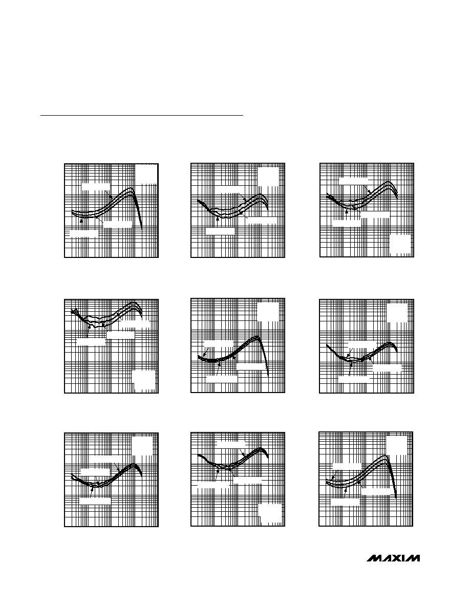
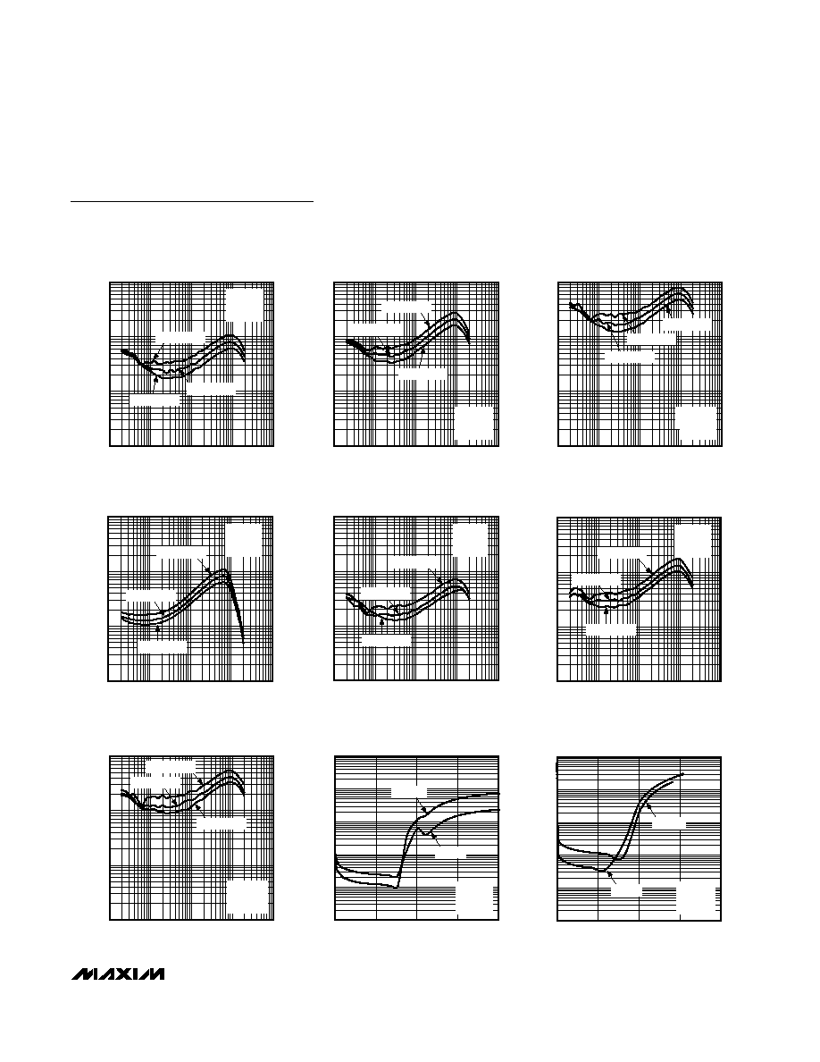
Typical Operating Characteristics
(Bridge-Tied Load, THD+N Bandwidth = 22Hz to 22kHz, C
BIAS
= 1µF.)
TOTAL HARMONIC DISTORTION PLUS NOISE
vs. FREQUENCY
MAX4366 toc01
FREQUENCY (Hz)
THD+N (%)
10k
1k
100
0.01
0.1
1
0.001
10
100k
V
CC
= 5V
A
V
= 2V/V
R
L
= 16
P
OUT
= 10mW
P
OUT
= 60mW
P
OUT
= 25mW
TOTAL HARMONIC DISTORTION PLUS NOISE
vs. FREQUENCY
MAX4366 toc02
FREQUENCY (Hz)
THD+N (%)
10k
1k
100
0.01
0.1
1
0.001
10
100k
V
CC
= 5V
A
V
= 3V/V
R
L
= 16
P
OUT
= 10mW
P
OUT
= 60mW
P
OUT
= 25mW
TOTAL HARMONIC DISTORTION PLUS NOISE
vs. FREQUENCY
MAX4366 toc03
FREQUENCY (Hz)
THD+N (%)
10k
1k
100
0.01
0.1
1
0.001
10
100k
P
OUT
= 10mW
P
OUT
= 60mW
P
OUT
= 25mW
V
CC
= 5V
A
V
= 4V/V
R
L
= 16
MAX4366 toc04
FREQUENCY (Hz)
THD+N (%)
10k
1k
100
0.01
0.1
1
0.001
10
100k
P
OUT
= 10mW
P
OUT
= 60mW
P
OUT
= 25mW
V
CC
= 5V
A
V
= 20V/V
R
L
= 16
TOTAL HARMONIC DISTORTION PLUS NOISE
vs. FREQUENCY
MAX4366 toc05
FREQUENCY (Hz)
THD+N (%)
10k
1k
100
0.01
0.1
1
0.001
10
100k
P
OUT
= 75mW
P
OUT
= 120mW
P
OUT
= 50mW
V
CC
= 5V
A
V
= 2V/V
R
L
= 32
TOTAL HARMONIC DISTORTION PLUS NOISE
vs. FREQUENCY
MAX4366 toc06
FREQUENCY (Hz)
THD+N (%)
10k
1k
100
0.01
0.1
1
0.001
10
100k
P
OUT
= 75mW
P
OUT
= 120mW
P
OUT
= 50mW
V
CC
= 5V
A
V
= 3V/V
R
L
= 32
TOTAL HARMONIC DISTORTION PLUS NOISE
vs. FREQUENCY
MAX4366 toc07
FREQUENCY (Hz)
THD+N (%)
10k
1k
100
0.01
0.1
1
0.001
10
100k
P
OUT
= 75mW
P
OUT
= 120mW
P
OUT
= 50mW
V
CC
= 5V
A
V
= 4V/V
R
L
= 32
TOTAL HARMONIC DISTORTION PLUS NOISE
vs. FREQUENCY
MAX4366 toc08
FREQUENCY (Hz)
THD+N (%)
10k
1k
100
0.01
0.1
1
0.001
10
100k
P
OUT
= 75mW
V
CC
= 5V
A
V
= 20V/V
R
L
= 32
P
OUT
= 120mW
P
OUT
= 50mW
TOTAL HARMONIC DISTORTION PLUS NOISE
vs. FREQUENCY
MAX4366 toc09
FREQUENCY (Hz)
THD+N (%)
10k
1k
100
0.01
0.1
1
0.001
10
100k
P
OUT
= 25mW
P
OUT
= 10mW
P
OUT
= 60mW
V
CC
= 3V
A
V
= 2V/V
R
L
= 16
TOTAL HARMONIC DISTORTION PLUS NOISE
vs. FREQUENCY
MAX4366/MAX4367/MAX4368
330mW, Ultra-Small, Audio Power Amplifiers
with Shutdown
_______________________________________________________________________________________
5
MAX4366 toc10
FREQUENCY (Hz)
THD+N (%)
10k
1k
100
0.01
0.1
1
0.001
10
100k
P
OUT
= 25mW
P
OUT
= 10mW
P
OUT
= 60mW
V
CC
= 3V
A
V
= 3V/V
R
L
= 16
TOTAL HARMONIC DISTORTION PLUS NOISE
vs. FREQUENCY
MAX4366 toc11
FREQUENCY (Hz)
THD+N (%)
10k
1k
100
0.01
0.1
1
0.001
10
100k
V
CC
= 3V
A
V
= 4V/V
R
L
= 16
P
OUT
= 60mW
P
OUT
= 10mW
P
OUT
= 25mW
TOTAL HARMONIC DISTORTION PLUS NOISE
vs. FREQUENCY
MAX4366 toc12
FREQUENCY (Hz)
THD+N (%)
10k
1k
100
0.01
0.1
1
0.001
10
100k
P
OUT
= 60mW
V
CC
= 3V
A
V
= 20V/V
R
L
= 16
P
OUT
= 10mW
P
OUT
= 25mW
TOTAL HARMONIC DISTORTION PLUS NOISE
vs. FREQUENCY
MAX4366 toc13
FREQUENCY (Hz)
THD+N (%)
10k
1k
100
0.01
0.1
1
0.001
10
100k
V
CC
= 3V
A
V
= 2V/V
R
L
= 32
P
OUT
= 10mW
P
OUT
= 50mW
P
OUT
= 25mW
TOTAL HARMONIC DISTORTION PLUS NOISE
vs. FREQUENCY
MAX4366 toc14
FREQUENCY (Hz)
THD+N (%)
10k
1k
100
0.01
0.1
1
0.001
10
100k
V
CC
= 3V
A
V
= 3V/V
R
L
= 32
P
OUT
= 10mW
P
OUT
= 50mW
P
OUT
= 25mW
TOTAL HARMONIC DISTORTION PLUS NOISE
vs. FREQUENCY
MAX4366 toc15
FREQUENCY (Hz)
THD+N (%)
10k
1k
100
0.01
0.1
1
0.001
10
100k
V
CC
= 3V
A
V
= 4V/V
R
L
= 32
P
OUT
= 10mW
P
OUT
= 50mW
P
OUT
= 25mW
TOTAL HARMONIC DISTORTION PLUS NOISE
vs. FREQUENCY
MAX4366 toc16
FREQUENCY (Hz)
THD+N (%)
10k
1k
100
0.01
0.1
1
0.001
10
100k
V
CC
= 3V
A
V
= 20V/V
R
L
= 32
P
OUT
= 10mW
P
OUT
= 50mW
P
OUT
= 25mW
TOTAL HARMONIC DISTORTION PLUS NOISE
vs. FREQUENCY
MAX4366 toc17
OUTPUT POWER (mW)
THD+N (%)
300
200
100
0.01
0.1
1
10
100
0.001
0
400
V
CC
= 5V
A
V
= 2V/V
R
L
= 16
f = 10kHz
f = 1kHz
TOTAL HARMONIC DISTORTION PLUS NOISE
vs. OUTPUT POWER
MAX4366 toc18
OUTPUT POWER (mW)
THD+N (%)
300
200
100
0.01
0.1
1
10
100
0.001
0
400
V
CC
= 5V
A
V
= 4V/V
R
L
= 16
f = 10kHz
f = 1kHz
TOTAL HARMONIC DISTORTION PLUS NOISE
vs. OUTPUT POWER
Typical Operating Characteristics (continued)
(Bridge-Tied Load, THD+N Bandwidth = 22Hz to 22kHz, C
BIAS
= 1µF.)