 | –≠–ª–µ–∫—Ç—Ä–æ–Ω–Ω—ã–π –∫–æ–º–ø–æ–Ω–µ–Ω—Ç: MAX4491 | –°–∫–∞—á–∞—Ç—å:  PDF PDF  ZIP ZIP |

For free samples and the latest literature, visit www.maxim-ic.com or phone 1-800-998-8800.
For small orders, phone 1-800-835-8769.
General Description
The MAX4490/MAX4491/MAX4492 single/dual/quad,
low-cost CMOS op amps feature Rail-to-Rail
Æ
input and
output capability from either a single +2.7V to +5.5V
supply or dual ±1.35V to ±2.75V supplies. These ampli-
fiers exhibit a high slew rate of 10V/µs and a gain-band-
width product of 10MHz. They can drive 2k
resistive
loads to within 55mV of either supply rail and remain
unity-gain stable with capacitive loads up to 300pF.
The MAX4490 is offered in the ultra-small, 5-pin SC70
package, which is 50% smaller than the standard 5-pin
SOT23 package. Specifications for all parts are guaran-
teed over the automotive (-40∞C to +125∞C) tempera-
ture range.
Applications
Battery-Powered Instruments
Portable Equipment
Audio Signal Conditioning
Low-Power/Low-Voltage Applications
Sensor Amplifiers
RF Power Amplifier Control
High-Side/Low-Side Current Sensors
Features
o
+2.7V to +5.5V Single-Supply Operation
o
10V/µs Slew Rate
o
Rail-to-Rail Input Common-Mode Voltage Range
o
Rail-to-Rail Output Voltage Swing
o
10MHz Gain-Bandwidth Product
o
Unity-Gain Stable with Capacitive Loads
Up to 300pF
o
50pA Input Bias Current
o
Ultra-Small, 5-Pin SC70 Package (MAX4490)
MAX4490/MAX4491/MAX4492
Low-Cost, High-Slew-Rate,
Rail-to-Rail I/O Op Amps in SC70
________________________________________________________________
Maxim Integrated Products
1
19-1525; Rev 1; 1/00
PART
MAX4490
AXK-T
MAX4490AUK-T
MAX4491
AKA-T -40∞C to +125∞C
-40∞C to +125∞C
-40∞C to +125∞C
TEMP. RANGE
PIN-
PACKAGE
5 SC70-5
5 SOT23-5
8 SOT23-8
Capacitive Load Stability
Ordering Information
Rail-to-Rail is a registered trademark of Nippon Motorola, Ltd.
MAX4492
AUD
-40∞C to +125∞C
14 TSSOP
MAX4492ASD
-40∞C to +125∞C
14 SO
TOP
MARK
AAB
ADKQ
AADB
--
--
0
100
100k
10k
1k
2000
4000
3000
6000
1000
5000
RESISTIVE LOAD (
)
CAPACITIVE LOAD (pF)
UNSTABLE
STABLE
Pin Configurations/
Functional Diagrams
Pin Configurations continued at end of data sheet.
V
SS
OUT
IN-
1
5
V
DD
IN+
MAX4490
SOT23-5/SC70-5
2
3
4
- +
TOP VIEW

MAX4490/MAX4491/MAX4492
Low-Cost, High-Slew-Rate,
Rail-to-Rail I/O Op Amps in SC70
2
_______________________________________________________________________________________
ABSOLUTE MAXIMUM RATINGS
ELECTRICAL CHARACTERISTICS
(V
DD
= +5V, V
SS
= 0, V
CM
= 0, V
OUT
= V
DD
/2, R
L
= 100k
connected to V
DD
/2, T
A
= T
MIN
to T
MAX
, unless otherwise noted. Typical
values are at T
A
= +25∞C.) (Note 1)
Stresses beyond those listed under "Absolute Maximum Ratings" may cause permanent damage to the device. These are stress ratings only, and functional
operation of the device at these or any other conditions beyond those indicated in the operational sections of the specifications is not implied. Exposure to
absolute maximum rating conditions for extended periods may affect device reliability.
Supply Voltage (V
DD
to V
SS
)..................................................+6V
All Other Pins ...................................(V
SS
- 0.3V) to (V
DD
+ 0.3V)
Output Short-Circuit Duration .................................................10s
Continuous Power Dissipation (T
A
= +70∞C)
5-Pin SC70 (derate 2.5mW/∞C above +70∞C) ............ 200mW
5-Pin SOT23 (derate 7.1mW/∞C above +70∞C).......... 571mW
8-Pin SOT23 (derate 5.26mW/∞C above +70∞C)........421 mW
14-Pin TSSOP (derate 8.3mW/∞C above +70∞C) ....... 667mW
14-Pin SO (derate 8.3mW/∞C above +70∞C).............. 667mW
Operating Temperature Range ........................ -40∞C to +125∞C
Junction Temperature ..................................................... +150∞C
Storage Temperature Range ............................ -65∞C to +150∞C
Lead Temperature (soldering, 10s) ................................ +300∞C
A
V(CL)
= 1, no sustained oscillations
= 10kHz
T
A
= +25∞C
= 10kHz
Measured from 10% to 90% of 4Vp-p step
(Note 2)
C
L
= 10pF
C
L
= 10pF
R
L
= 100k
2.7V
V
DD
5.5V
C
L
= 10pF
V
SS
V
CM
V
DD
Inferred from CMRR test
T
A
= T
MIN
to T
MAX
(Note 3)
(Note 3)
Sourcing or sinking
R
L
= 2k
CONDITIONS
pF
300
Capacitive Load Drive
fA
Hz
1
i
n
Current Noise Density
nV/
Hz
12
e
n
Voltage Noise Density
V/µs
10
SR
Slew Rate
dB
10
Gain Margin
deg
60
Phase Margin
pF
5
C
IN
Input Capacitance
MHz
10
GBWP
Gain-Bandwidth Product
mA
±50
I
OUT(SC)
Output Short-Circuit Current
65
85
mV
±1.5
±10
V
OS
Input Offset Voltage
mA
0.8
2
I
S
V
2.7
5.5
V
DD
Supply Voltage Range
Supply Current (per amplifier)
dB
110
A
V
Large-Signal Voltage Gain
dB
65
100
PSRR
Power-Supply Rejection Ratio
dB
54
75
CMRR
Common-Mode Rejection Ratio
V
V
SS
V
DD
V
CM
Input Common-Mode Range
16
nA
±0.05
±2.5
I
B
Input Bias Current
nA
±0.05
±2.5
I
OS
Input Offset Current
M
1000
R
IN
Input Resistance
UNITS
MIN
TYP
MAX
SYMBOL
PARAMETER
Note 1:
All units production tested at T
A
= +25∞C. Limits over temperature guaranteed by design.
Note 2:
Guaranteed by the Power-Supply Rejection Ratio (PSRR) test.
Note 3:
Input Offset Voltage, Input Bias Current, and Input Offset Current are all tested and guaranteed at both ends of the common-
mode range.
(V
SS
+ 0.25V)
V
OUT
(V
DD
- 0.25V)
R
L
= 100k
R
L
= 2k
55
200
mV
1.5
V
OH
Output Voltage Swing High
Specified as
V
DD
- V
OH
R
L
= 100k
R
L
= 2k
35
150
mV
1.5
V
OL
Output Voltage Swing Low
Specified as
V
OL
- V
SS
(Note 3)

MAX4490/MAX4491/MAX4492
Low-Cost, High-Slew-Rate,
Rail-to-Rail I/O Op Amps in SC70
_______________________________________________________________________________________
3
500
600
550
700
650
800
750
850
-40
-10 5
20
-25
35 50 65 80 95 110 125
SUPPLY CURRENT PER AMPLIFIER
vs. TEMPERATURE
MAX4490 toc 01
TEMPERATURE (∞C)
SUPPLY CURRENT (
µ
A)
V
DD
= +5.0V
V
DD
= +2.7V
0
300
200
100
500
400
900
800
700
600
1000
2.0
2.5
3.0
3.5
4.0
4.5
5.0
5.5
SUPPLY CURRENT PER AMPLIFIER
vs. SUPPLY VOLTAGE
MAX4490
toc02
SUPPLY VOLTAGE (V)
SUPPLY CURRENT (
µ
A)
-2.0
-1.4
-1.6
-1.8
-1.0
-1.2
-0.2
-0.4
-0.6
-0.8
0
-40 -25 -10 5
20 35 50
80
65
95
125
110
INPUT OFFSET VOLTAGE
vs. TEMPERATURE
MAX4490 toc03
TEMPERATURE (
∞
C)
OFFSET VOLTAGE (mV)
0
20
10
30
60
70
50
40
80
-40
-10
5
20 35
-25
50 65 80 95 110 125
OUTPUT SWING HIGH
vs. TEMPERATURE
MAX4490 toc04
TEMPERATURE (∞C)
V
DD
- V
OUT
(mV)
V
DD
= +5.0V
R
L
= 2k
V
DD
= +2.7V
R
L
= 2k
V
DD
= +5.0V OR +2.7V
R
L
= 100k
0
20
10
30
60
70
50
40
80
-40
-10
5
20 35
-25
50 65 80 95 110 125
OUTPUT SWING LOW
vs. TEMPERATURE
MAX4490 toc05
TEMPERATURE (∞C)
V
OUT
- V
SS
(mV)
V
DD
= +5.0V
R
L
= 2k
V
DD
= +2.7V
R
L
= 2k
V
DD
= +5.0V OR +2.7V
R
L
= 100k
-20
0
-10
10
40
50
30
20
60
100
1k
10k
100k
1M
10M
OP AMP GAIN AND PHASE
vs. FREQUENCY
FREQUENCY (Hz)
GAIN (dB)
-180
-90
-135
-45
90
135
45
0
180
PHASE (DEGREES)
MAX4490 toc06
GAIN
PHASE
A
V
= +1000
C
L
= 10pF
-20
0
-10
10
40
50
30
20
60
100
1k
10k
100k
1M
10M
GAIN AND PHASE
vs. FREQUENCY (WITH C
LOAD
)
MAX4490 toc07
FREQUENCY (Hz)
GAIN (dB)
A
V
= +1000
C
LOAD
= 200pF
-180
-90
-135
-45
90
135
45
0
180
PHASE (DEGREES)
GAIN
PHASE
80
90
100
110
120
130
-40
-10 5
-25
20 35 50 65 80 95 110 125
LARGE-SIGNAL GAIN
vs. TEMPERATURE
MAX4490 toc08
TEMPERATURE (∞C)
LARGE-SIGNAL GAIN (dB)
V
DD
= 5.0V
-100
-70
-60
-90
-80
-30
-40
-50
-10
-20
0
10
1k
10k
100
100k
1M
10M
POWER-SUPPLY REJECTION RATIO
vs. FREQUENCY
MAX4490 toc09
FREQUENCY (Hz)
PSSR (dB)
A
V
= +1
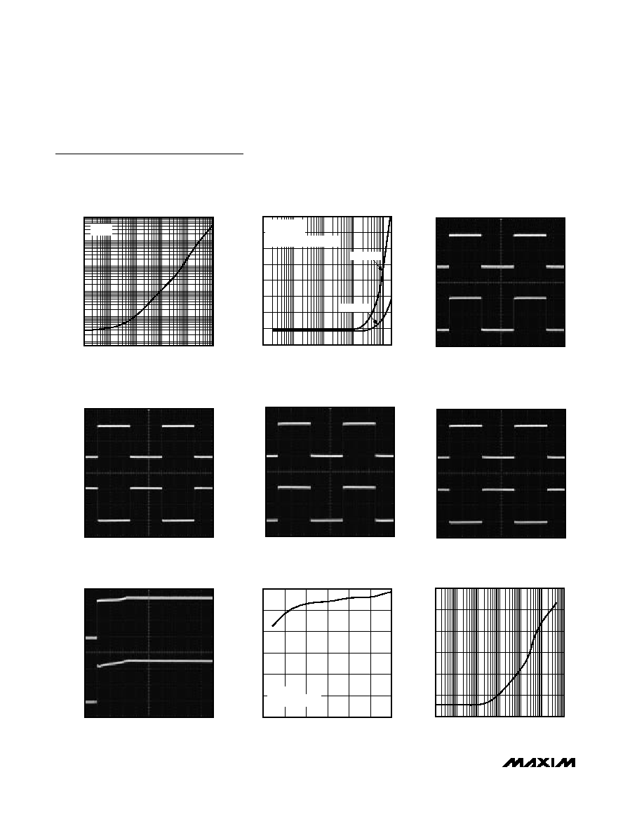
Typical Operating Characteristics
(V
DD
= +5V, V
SS
= 0, V
CM
= V
DD
/2, R
L
= 100k
to V
DD
/2, T
A
= +25∞C, unless otherwise noted.)
MAX4490/MAX4491/MAX4492
Low-Cost, High-Slew-Rate,
Rail-to-Rail I/O Op Amps in SC70
4
_______________________________________________________________________________________
Typical Operating Characteristics (continued)
(V
DD
= +5V, V
SS
= 0, V
CM
= V
DD
/2, R
L
= 100k
to V
DD
/2, T
A
= +25∞C, unless otherwise noted.)
0.01
1
0.1
10
100
1k
1k
10k
100
100k
1M
10M
OUTPUT IMPEDANCE vs. FREQUENCY
MAX4490 toc10
FREQUENCY (Hz)
OUTPUT IMPEDANCE (
)
A
V
= +1
0.040
0
10
100
1k
10k
100k
TOTAL HARMONIC DISTORTION PLUS
NOISE vs. FREQUENCY
0.005
0.010
MAX4490 toc11
FREQUENCY (Hz)
THD + NOISE (%) 0.015
0.020
0.025
0.030
0.035
A
V
= +1V/V
2Vp-p SIGNAL
500kHz LOWPASS FILTER
R
L
= 2k
R
L
= 10k
LARGE-SIGNAL TRANSIENT RESPONSE
(NONINVERTING)
A
V
= +1
IN
OUT
40
µ
s/div
2V/div
2V/div
MAX4490toc12
LARGE-SIGNAL TRANSIENT RESPONSE
(INVERTING)
A
V
= -1
IN
OUT
2V/div
2V/div
40
µ
s/div
MAX4490toc13
SMALL-SIGNAL TRANSIENT RESPONSE
(NONINVERTING)
A
V
= +1
40
µ
s/div
IN
OUT
50mV/div
50mV/div
MAX4490toc14
SMALL-SIGNAL TRANSIENT RESPONSE
(INVERTING)
A
V
= -1
IN
OUT
40
µ
s/div
MAX4490toc15
50mV/div
50mV/div
POWER-UP TRANSIENT RESPONSE
A
V
= +1, V
IN
CONNECTED TO V
DD
/2, R
L
= 2k
V
DD
OUT
2V/div
1V/div
MAX4490toc16
4
µ
s/div
0
4
2
8
6
10
12
2.5
3.5
4.0
3.0
4.5
5.0
5.5
SLEW RATE vs. SUPPLY VOLTAGE
MAX4490 toc17
SUPPLY VOLTAGE (V)
SLEW RATE (V/
µ
S)
A
V
= +1
10% TO 90% STEP
0
-20
-40
-120
0.001
1
10
100
0.01
0.1
1000
MAX4491/MAX4492
CROSSTALK vs. FREQUENCY
-60
-80
-100
MAX4492toc18
FREQUENCY (MHz)
CROSSTALK (dB)
MAX4490/MAX4491/MAX4492
Low-Cost, High-Slew-Rate,
Rail-to-Rail I/O Op Amps in SC70
_______________________________________________________________________________________
5
NAME
FUNCTION
MAX4490
1
IN+
Noninverting Input
PIN
2
V
SS
Negative Supply Input. Connect to ground for single-supply operation.
3
IN-
Inverting Input
≠
INA-
Inverting Input to Amplifier A
≠
INA+
Noninverting Input to Amplifier A
5
V
DD
Positive Supply Input
4
OUT
Amplifier Output
≠
INC+, IND+
Noninverting Inputs to Amplifiers C and D
≠
OUTB
Amplifier B Output
≠
INB-
Inverting Input to Amplifier B
≠
INB+
Noninverting Input to Amplifier B
≠
OUTA
Amplifier A Output
Pin Description
MAX4492
≠
11
≠
2
3
4
≠
10, 12
7
6
5
1
MAX4491
≠
4
≠
2
3
8
≠
≠
7
6
5
1
≠
≠
9, 13
INC-, IND-
Inverting Inputs to Amplifiers C and D
≠
≠
8, 14
OUTC, OUTD
Amplifiers C and D Outputs
Detailed Description
Rail-to-Rail Input Stage
The MAX4490/MAX4491/MAX4492 CMOS operational
amplifiers have parallel-connected N- and P-channel
differential input stages that combine to accept a com-
mon-mode range extending to both supply rails. The N-
channel stage is active for common-mode input
voltages typically greater than (V
SS
+ 1.2V), and the P-
channel stage is active for common-mode input volt-
ages typically less than (V
DD
- 1.2V).
Rail-to-Rail Output Stage
The MAX4490/MAX4491/MAX4492 CMOS operational
amplifiers feature class-AB push-pull output stages that
can drive a 100k
load to within 1.5mV of either supply
rail. Short-circuit output current is typically ±50mA.
Figures 1a and 1b show the typical temperature depen-
dence of output source and sink currents, respectively,
for three fixed values of (V
DD
- V
OH
) and (V
OL
- V
SS
).
For example, at V
DD
= +5.0V, the load currents that
maintain (V
DD
- V
OH
) = 100mV and (V
OL
- V
SS
) = 100mV
at T
A
= +25∞C are 2.2mA and 3.3mA, respectively,
when the load is connected to V
DD
/2. Consistent resis-
tive drive capability is (2.5 - 0.1) / 2.2 = 1.1k
. For the
same application, resistive drive capability is 2.2k
when the load is connected to V
DD
or V
SS
.
Applications Information
Power-Supply Considerations
The MAX4490/MAX4491/MAX4492 operate from a sin-
gle +2.7V to +5.5V supply or from dual ±1.35V to
±2.75V supplies with typically 800µA supply current
per amplifier. A high power-supply rejection ratio of
100dB allows for extended operation from a decaying
battery voltage, thereby simplifying designs for
portable applications. For single-supply operation,
bypass the power supply with a 0.1µF ceramic capaci-
tor placed close to the V
DD
pin. For dual-supply opera-
tion, bypass each supply to ground.
Input Capacitance
One consequence of the parallel-connected differential
input stages for rail-to-rail operation is a relatively large
input capacitance C
IN
(typically 5pF). This introduces a