
For pricing delivery, and ordering information please contact Maxim/Dallas Direct! at
1-888-629-4642, or visit Maxim's website at www.maxim-ic.com.
General Description
The MAX4541≠MAX4544 are precision, dual analog
switches designed to operate from a single +2.7V to +12V
supply. Low power consumption (5µW) makes these parts
ideal for battery-powered equipment. These switches offer
low leakage currents (100pA max) and fast switching
speeds (t
ON
= 150ns max, t
OFF
= 100ns max).
When powered from a +5V supply, the MAX4541≠
MAX4544 offer 2
max matching between channels, 60
max on-resistance (R
ON
), and 6
max R
ON
flatness.
These switches also offer 5pC max charge injection and
a minimum of 2000V ESD protection per Method 3015.7.
The MAX4541/MAX4542/MAX4543 are dual single-pole/
single-throw (SPST) devices and the MAX4544 is a single-
pole/double-throw (SPDT) device. The MAX4541 has two
normally open (NO) switches and the MAX4542 has two
normally closed (NC) switches. The MAX4543 has one NO
and one NC switch and can be used as an SPDT, while
the MAX4544 is an SPDT. The MAX4541/MAX4542/
MAX4543 are available in tiny SOT23-8 and QFN-8 pack-
ages, and the MAX4544 is available in a SOT23-6 package.
________________________Applications
____________________________Features
o Low R
ON
: 60
max (33 typ)
o R
ON
Matching Between Channels: 2
max
o R
ON
Flatness: 6
max
o Guaranteed Charge Injection: 5pC max
o +2.7V to +12V Single-Supply Operation
o Low Power Consumption: <5µW
o Low Leakage Current Over Temperature:
10nA max at +85∞C
o Fast Switching: t
ON
= 35ns, t
OFF
= 25ns
o Guaranteed Break-Before-Make
(MAX4543/MAX4544 only)
o TTL/CMOS-Logic Compatible
o Pin Compatible with MAX323/MAX324/MAX325
o MAX4541/42/43 Available in SOT23-8
MAX4544 Available in SOT23-6
MAX4541≠MAX4544
Low-Voltage, Single-Supply
Dual SPST/SPDT Analog Switches
________________________________________________________________ Maxim Integrated Products
1
19-1202; Rev 3; 8/02
Ordering Information continued at end of data sheet.
*Dice are specified at T
A
= +25∞C.
Ordering Information
Pin Configurations/Functional Diagrams/Truth Tables
µMAX/SO/DIP/QFN
8
7
6
5
1
2
3
4
V+
PIN 6
IN
N.C.
N.C.
GND
NC
COM
NO
MAX4544
SOT23-6*
6
5
4
1
2
3
NO
COM
NC
GND
V+
IN
6
AAAM
5
4
1
2
3
MAX4544
MAX4544
SWITCHES SHOWN FOR "0" INPUT
N.C. = NOT INTERNALLY CONNECTED
MAX4541/MAX4542/MAX4543
APPEAR AT END OF DATA SHEET.
*NOTE: SOT23-6 PACKAGE
HAS LETTERING NEAREST PIN 6
TOP VIEW
MAX4544
LOGIC
NC
0
1
ON
OFF
NO
OFF
ON
Battery-Operated Systems
Sample-and-Hold Circuits
Heads-Up Displays
Guidance and Control
Systems
Audio and Video
Switching
Military Radios
Test Equipment
Communications Systems
+3V/+5V DACs and ADCs
PBX, PABX
Cell Phones
Ultrasound
Pagers
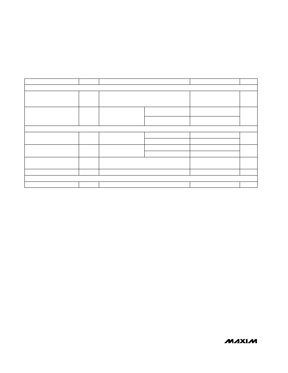
PART
TEMP RANGE
PIN-
PACKAGE
TOP
MARK
MAX4541CUA
0∞C to +70∞C
8 µMAX
--
MAX4541CSA
0∞C to +70∞C
8 SO
--
MAX4541CPA
0∞C to +70∞C
8 Plastic DIP
--
MAX4541C/D
0∞C to +70∞C
Dice*
--
MAX4541EKA-T
-40∞C to +85∞C
8 SOT23-8
AAAE
MAX4541EGA
-40∞C to +85∞C
8 QFN
--
MAX4541EUA
-40∞C to +85∞C
8 µMAX
--
MAX4541ESA
-40∞C to +85∞C
8 SO
--

MAX4541≠MAX4544
Low-Voltage, Single-Supply
Dual SPST/SPDT Analog Switches
2
_______________________________________________________________________________________
Voltage Referenced to GND
V+ .........................................................................-0.3V to +13V
IN_, COM_, NC_, NO_ (Note 1)..................-0.3V to (V+ + 0.3V)
Continuous Current (any terminal)....................................±10mA
Peak Current, COM_, NO_, NC_
(pulsed at 1ms, 10% duty cycle max) ............................±20mA
ESD per Method 3015.7 ..................................................>2000V
Continuous Power Dissipation
SOT23-6 (derate 7.1mW/∞C above +70∞C)....................571mW
SOT23-8 (derate 5.3mW/∞C above +70∞C)....................421mW
QFN (derate 24.4mW/∞C above +70∞C) ......................1951mW
µMAX (derate 4.10mW/∞C above +70∞C) ......................330mW
Narrow SO (derate 5.88mW/∞C above +70∞C) ..............471mW
Plastic DIP (derate 9.09mW/∞C above +70∞C) ..............727mW
Operating Temperature Ranges
MAX454_C_ _ .......................................................0∞C to +70∞C
MAX454_E_ _.....................................................-40∞C to +85∞C
Storage Temperature Range .............................-65∞C to +150∞C
Lead Temperature (soldering, 10s) .................................+300∞C
Stresses beyond those listed under "Absolute Maximum Ratings" may cause permanent damage to the device. These are stress ratings only, and functional
operation of the device at these or any other conditions beyond those indicated in the operational sections of the specifications is not implied. Exposure to
absolute maximum rating conditions for extended periods may affect device reliability.
ABSOLUTE MAXIMUM RATINGS
ELECTRICAL CHARACTERISTICS--Single +5V Supply
(V+ = +5V ±10%, GND = 0, V
INH
= 2.4V, V
INL
= 0.8V, T
A
= T
MIN
to T
MAX
, unless otherwise noted.) (Notes 2, 3)
Note 1: Signals on NC, NO, COM, or IN exceeding V+ or V- are clamped by internal diodes. Limit forward diode current to maximum
current rating.
COM On-Leakage Current
(Note 7)
I
COM(ON)
V+ = 5.5V;
V
COM
= 1V, 4.5V or
V
NO
or V
NC
= 1V, 4.5V,
or floating
nA
COM Off-Leakage Current
(Note 7)
I
COM(OFF)
V+ = 5.5V;
V
COM
= 4.5V, 1V;
V
NO
or V
NC
= 1V, 4.5V
nA
NO or NC Off-Leakage
Current (Note 7)
I
NO(OFF)
or
I
NC(OFF)
V+ = 5.5V;
V
COM
= 1V, 4.5V;
V
NO
or V
NC
= 4.5V, 1V
nA
-10
10
C, E
C, E
C, E
T
A
= T
MIN
to T
MAX
T
A
= T
MIN
to T
MAX
T
A
= T
MIN
to T
MAX
-5
5
8
4
75
-5
5
-0.2
0.2
-0.1
0.1
-0.1
0.01
0.1
V+ = 5V;
I
COM
= 1.0mA;
V
NO
or V
NC
= 1V, 2V, 3V
2
6
R
FLAT(ON)
On-Resistance Flatness
(Note 6)
V+ = 5V,
I
COM
= 1.0mA,
V
NO
or V
NC
= 3.5V
0.8
2
R
ON
On-Resistance Match
Between Channels (Note 5)
T
A
= T
MIN
to T
MAX
T
A
= T
MIN
to T
MAX
T
A
= T
MIN
to T
MAX
T
A
= +25∞C
T
A
= +25∞C
T
A
= +25∞C
T
A
= +25∞C
T
A
= +25∞C
T
A
= +25∞C
V+ = 4.5V,
I
COM
= 1.0mA,
V
NO
or V
NC
= 3.5V
30
60
R
ON
On-Resistance
(Note 4)
CONDITIONS
V
0
V+
V
COM,
V
NO,
V
NC
Analog Signal Range
UNITS
MIN
TYP
MAX
SYMBOL
PARAMETER
ANALOG SWITCH

MAX4541≠MAX4544
Low-Voltage, Single-Supply
Dual SPST/SPDT Analog Switches
_______________________________________________________________________________________
3
ELECTRICAL CHARACTERISTICS--Single +5V Supply (continued)
(V+ = +5V ±10%, GND = 0, V
INH
= 2.4V, V
INL
= 0.8V, T
A
= T
MIN
to T
MAX
, unless otherwise noted.) (Notes 2, 3)
MAX4544
MAX4541/2/3
20
f = 1MHz, T
A
= +25∞C,
Figure 7
pF
13
C
COM(ON)
COM On-Capacitance
V+ = 5.5V, V
IN
= 0 or V+, all channels on or off
µA
-1
0.0001
1
I+
Positive Supply Current
V
0.8
V
INL
Input Voltage Low
V
2.4
V
INH
Input Voltage High
f = 1MHz, T
A
= +25∞C, Figure 7
pF
8
C
COM(OFF)
COM Off-Capacitance
f = 1MHz, T
A
= +25∞C, Figure 7
pF
8
C
OFF
NC or NO Capacitance
R
L
= 50
, C
L
= 5pF, f = 1MHz, T
A
= +25∞C,
Figure 6
dB
-90
Crosstalk (Note 9)
R
L
= 50
, C
L
= 5pF, f = 1MHz, T
A
= +25∞C,
Figure 5
dB
-76
OIRR
Off-Isolation (Note 8)
150
240
T
A
= T
MIN
to T
MAX
T
A
= T
MIN
to T
MAX
T
A
= +25∞C
T
A
= +25∞C
C
L
= 1.0nF, V
GEN
= 0, R
GEN
= 0, T
A
= +25∞C,
Figure 4
pC
1
5
Q
Charge Injection
(Note 4)
V
2.7
12
V+
Power-Supply Range
V
NO
or V
NC
= 3V,
Figure 2
ns
25
75
t
OFF
Turn-Off Time
MAX4543/MAX4544 only, R
L
= 300
, C
L
= 35pF
ns
2
10
t
D
Break-Before-Make Time
Delay (Note 4)
V
NO
or V
NC
= 3V,
Figure 2
ns
35
100
t
ON
Turn-On Time
CONDITIONS
UNITS
MIN
TYP
MAX
SYMBOL
PARAMETER
DYNAMIC
SUPPLY
LOGIC INPUT
MAX4541≠MAX4544
Low-Voltage, Single-Supply
Dual SPST/SPDT Analog Switches
4
_______________________________________________________________________________________
ELECTRICAL CHARACTERISTICS--Single +3.3V Supply
(V+ = +3.0V to +3.6V, GND = 0, V
INH
= 2.4V, V
INL
= 0.8V, T
A
= T
MIN
to T
MAX
, unless otherwise noted.) (Notes 2, 3)
Note 2: QFN and SOT-packaged parts are 100% tested at +25∞C only and guaranteed by correlation at the full hot rated temperature.
Note 3: The algebraic convention, where the most negative value is a minimum and the most positive value a maximum, is used in
this data sheet.
Note 4: Guaranteed by design.
Note 5:
R
ON
=
R
ON
max -
R
ON
min.
Note 6: Flatness is defined as the difference between the maximum and minimum value of on-resistance as measured over the
specified analog signal range.
Note 7: Leakage parameters are 100% tested at maximum rated hot temperature and guaranteed by correlation at +25∞C.
Note 8: Off Isolation = 20log
10
[V
COM
/ (V
NC
or V
NO)
], V
COM
= output, V
NC
or V
NO
= input to off switch.
Note 9: Between the two switches, MAX4541/MAX4542/MAX4543 only.
PARAMETER
SYMBOL
CONDITIONS
MIN
TYP
MAX
UNITS
Analog Signal Range
V
COM,
V
NO,
V
NC
(Note 3)
0
V+
V
Channel On-Resistance
R
ON
V+ = 3V,
I
COM
= 1.0mA,
V
NO
or V
NC
= 1.5V
275
Turn-On Time (Note 3)
t
ON
V
NO
or V
NC
= 1.5V
80
400
ns
500
Turn-Off Time (Note 3)
t
OFF
V
NO
or V
NC
= 1.5V
50
125
ns
175
Break-Before-Make Time
Delay (Note 3)
t
D
MAX4543/MAX4544 only, R
L
= 300
, C
L
= 35pF,
T
A
= +25∞C
2
30
ns
Charge Injection (Note 3)
Q
C
L
= 1.0nF, V
GEN
= 0, R
GEN
= 0, T
A
= +25∞C
1
5
pC
T
A
= T
MIN
to T
MAX
50
125
T
A
= +25∞C
T
A
= T
MIN
to T
MAX
T
A
= +25∞C
T
A
= +25∞C
T
A
= T
MIN
to T
MAX
Positive Supply Current
I+
V+ = 3.6V, V
IN
= 0 or V+, all channels on or off
-1
1
µA
ANALOG SWITCH
DYNAMIC
SUPPLY

MAX4541≠MAX4544
Low-Voltage, Single-Supply
Dual SPST/SPDT Analog Switches
_______________________________________________________________________________________
5
0
10
20
30
40
50
60
70
80
0
2
4
6
8
10
12
ON-RESISTANCE vs. COM VOLTAGE
MAX4541-01
V
COM
(V)
R
ON
(
)
A: V+ = +3V
B: V+ = +5V
C: V+ = +12V
A
B
C
0
10
20
30
40
50
60
0
1
2
3
4
5
ON-RESISTANCE vs.
COM VOLTAGE OVER TEMPERATURE
MAX4541-02
V
COM
(V)
R
ON
(
)
A: T
A
= +125∞C
B: T
A
= +85∞C
C: T
A
= +25∞C
D: T
A
= -40∞C
E: T
A
= -55∞C
A
B
C
D
E
0
20
40
60
80
100
120
140
160
180
200
0
2
4
6
8
10
12
TURN-ON/OFF TIMES vs.
SUPPLY VOLTAGE
MAX4541-03
V
SUPPLY
(V)
t
ON
/t
OFF
(ns)
t
ON
t
OFF
V+ = +5V
0
t
ON
t
OFF
10
20
30
40
50
60
70
80
90
100
TURN-ON/OFF TIMES
vs. TEMPERATURE
MAX4541-04
TEMPERATURE (∞C)
t
ON
/t
OFF
(ns)
-55 -35 -15
5
25
45
65
85 105 125
V+ = +5V
-100
-90
-80
-70
-60
-50
-40
-30
-20
-10
0
0.1
1
10
100
FREQUENCY RESPONSE
MAX4541-07
FREQUENCY (MHz)
LOSS (dB)
-225
-180
-135
-90
-45
0
45
90
135
180
225
PHASE (DEGREES)
ON-LOSS
ON-PHASE
OFF-LOSS
50
IN AND OUT
V+ = +5V
0.001
0.01
0.1
1
10
100
ON/OFF-LEAKAGE CURRENT
vs. TEMPERATURE
MAX4541-05
TEMPERATURE (∞C)
ON/OFF-LEAKAGE (nA)
-55
-30
-5
20
45
70
95
120 125
I
COM(ON)
V+ = +5.5V
I
COM
/I
N(OFF)
0
1
2
3
4
5
6
7
8
0
1
2
3
4
5
CHARGE INJECTION vs. COM VOLTAGE
MAX4541-06
V
COM
(V)
Q (pC)
V- = +5V
0
100
200
300
400
500
600
700
800
900
1000
INPUT VOLTAGE vs. SUPPLY CURRENT
MAX4541-08
V
IN
(V)
I+ (nA)
0
1
2
3
4
5
I
V+
10
0.1
1
100
1k
10k
TOTAL HARMONIC DISTORTION
vs. FREQUENCY
MAX4541-09
FREQUENCY (Hz)
THD (%)
__________________________________________Typical Operating Characteristics
(T
A
= +25∞C, unless otherwise noted.)