Äîêóìåíòàöèÿ è îïèñàíèÿ www.docs.chipfind.ru
________________General Description
The MAX4617/MAX4618/MAX4619 are high-speed, low-
voltage, CMOS analog ICs configured as an 8-channel
multiplexer (MAX4617), two 4-channel multiplexers
(MAX4618), and three single-pole/double-throw (SPDT)
switches (MAX4619).
These CMOS devices can operate continuously with a
+2V to +5.5V single supply. Each switch can handle
Rail-to-Rail
®
analog signals. The off-leakage current is
only 1nA at T
A
= +25°C and 10nA at T
A
= +85°C.
All digital inputs have 0.8V to 2.4V logic thresholds,
ensuring TTL/CMOS-logic compatibility when using a
single +5V supply.
________________________Applications
Battery-Operated Equipment
Audio/Video Signal Routing
Low-Voltage Data-Acquisition Systems
Communications Circuits
____________________________Features
o
Fast Switching Times
15ns t
ON
10ns t
OFF
o
Pin Compatible with Industry-Standard
74HC4051/74HC4052/74HC4053 and
MAX4581/MAX4582/MAX4583
o
Guaranteed On-Resistance
10
max (+5V Supply)
20
max (+3V Supply)
o
Guaranteed 1
On-Resistance Match Between
Channels (single +5V supply)
o
Guaranteed Low Off-Leakage Current:
1nA at +25°C
o
Guaranteed Low On-Leakage Current:
1nA at +25°C
o
+2V to +5.5V Single-Supply Operation
o
TTL/CMOS-Logic Compatible
o
Low Crosstalk: <-96dB
o
High Off-Isolation: <-93dB
o
Low Distortion: <0.017% (600
)
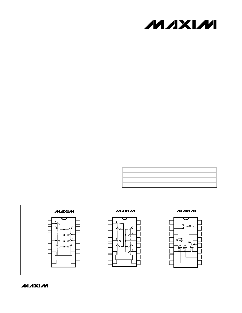
MAX4617/MAX4618/MAX4619
High-Speed, Low-Voltage, CMOS Analog
Multiplexers/Switches
________________________________________________________________
Maxim Integrated Products
1
16
15
14
13
12
11
10
9
1
2
3
4
5
6
7
8
V
CC
X2
X1
X0
X3
A
B
C
X4
X6
X
X7
X5
ENABLE
N.C.
GND
TOP VIEW
MAX4617
DIP/SO/TSSOP
LOGIC
16
15
14
13
12
11
10
9
1
2
3
4
5
6
7
8
V
CC
Y
X
X1
X0
A
B
C
Y1
Y0
Z1
Z
Z0
ENABLE
N.C.
GND
MAX4619
DIP/SO/TSSOP
16
15
14
13
12
11
10
9
1
2
3
4
5
6
7
8
V
CC
X2
X1
X
X0
X3
A
B
Y0
Y2
Y
Y3
Y1
ENABLE
N.C.
GND
MAX4618
DIP/SO/TSSOP
LOGIC
____________________________________Pin Configurations/Functional Diagrams
19-1502; Rev 0; 7/99
_______________Ordering Information
Ordering Information continued at end of data sheet.
Rail-to-Rail is a registered trademark of Nippon Motorola, Ltd.
For free samples & the latest literature: http://www.maxim-ic.com, or phone 1-800-998-8800.
For small orders, phone 1-800-835-8769.
16 Plastic DIP
16 Narrow SO
16 TSSOP
PIN-PACKAGE
TEMP. RANGE
0°C to +70°C
0°C to +70°C
0°C to +70°C
MAX4617CPE
MAX4617CSE
MAX4617
CUE
PART
MAX4617/MAX4618/MAX4619
High-Speed, Low-Voltage, CMOS Analog
Multiplexers/Switches
2
_______________________________________________________________________________________
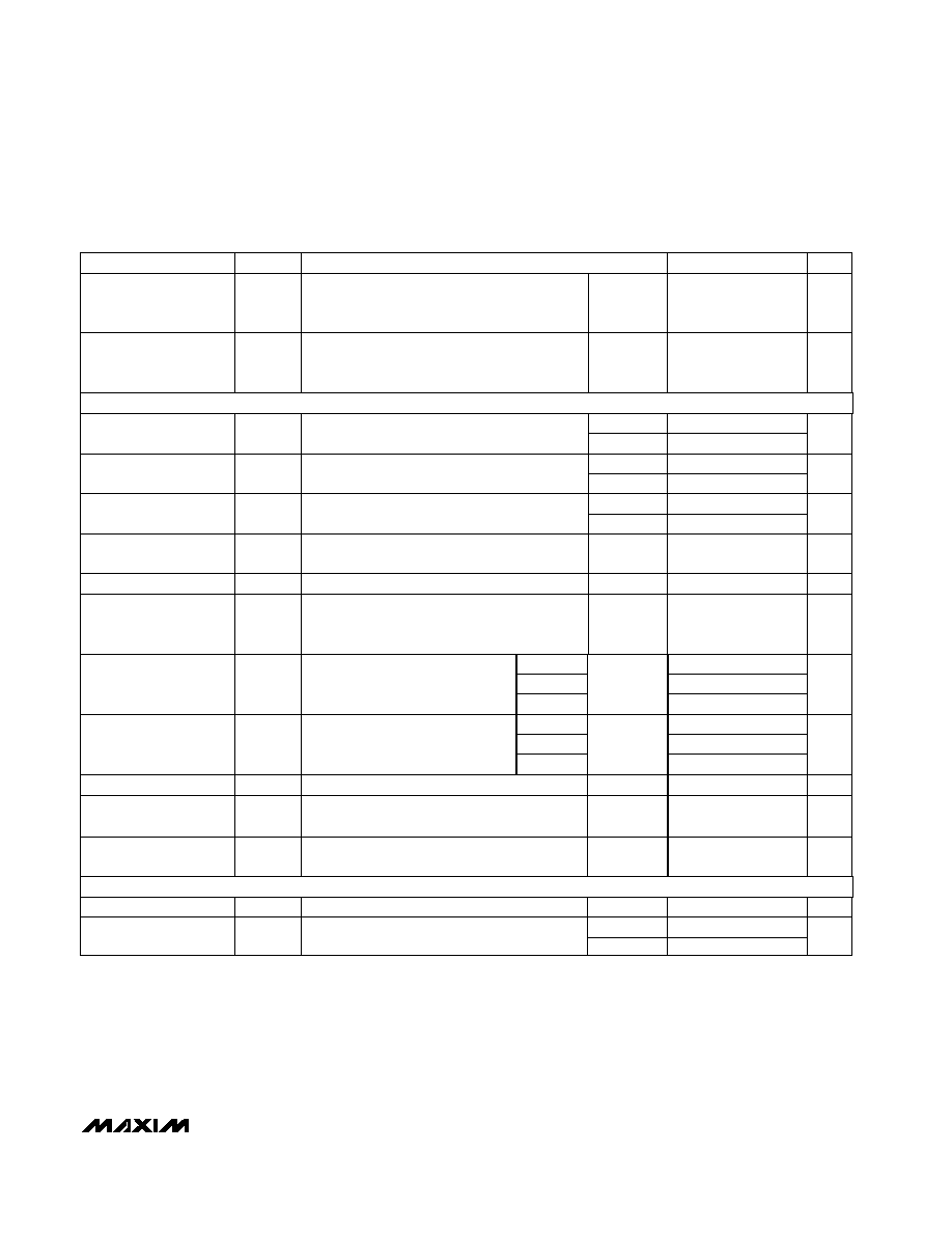
ABSOLUTE MAXIMUM RATINGS
ELECTRICAL CHARACTERISTICS--Single +5V Supply
(V
CC
= +4.5V to +5.5V, V
_H
= 2.4V, V
_L
= 0.8V, T
A
= T
MIN
to T
MAX
, unless otherwise noted. Typical values are at T
A
= +25°C.) (Note 2)
Stresses beyond those listed under "Absolute Maximum Ratings" may cause permanent damage to the device. These are stress ratings only, and functional
operation of the device at these or any other conditions beyond those indicated in the operational sections of the specifications is not implied. Exposure to
absolute maximum rating conditions for extended periods may affect device reliability.
Voltages Referenced to GND
V
CC,
A, B, C, or Enable...........................................-0.3V to +6V
Voltage into Any Analog Terminal
(Note 1) .........................................................-0.3V to (V
CC
+ 0.3V)
Continuous Current into Any Terminal..............................±75mA
Peak Current, X_, Y_, Z_
(pulsed at 1ms, 10% duty cycle) .................................±200mA
Continuous Power Dissipation (T
A
= +70°C)
TSSOP (derate 6.7mW/°C above +70°C) ......................533mW
Narrow SO (derate 8.70mW/°C above +70°C)..............696mW
Plastic DIP (derate 10.53mW/°C above +70°C) ..............842mW
Operating Temperature Ranges
MAX461_C_ _ ......................................................0°C to +70°C
MAX461_E_ _ ....................................................-40°C to +85°C
Storage Temperature Range .............................-65°C to +150°C
Lead Temperature (soldering, 10sec) .............................+300°C
Note 1:
Voltages exceeding V
CC
or GND on any analog signal terminal are clamped by internal diodes. Limit forward-diode current
to maximum current rating.
C, E
-10
10
-1
0.002
1
X, Y, Z On-Leakage
Current (Note 5)
I
X(ON)
,
I
Y(ON)
,
I
Z(ON)
nA
T
A
= +25°C
C, E
-10
10
-1
0.002
1
X, Y, Z Off-Leakage
Current (Note 5)
I
X(OFF)
,
I
Y(OFF)
,
I
Z(OFF)
nA
T
A
= +25°C
C, E
-10
10
-1
0.002
1
X_, Y_, Z_
Off-Leakage Current
(Note 5)
I
X_(OFF)
,
I
Y_(OFF)
,
I
Z_(OFF)
nA
T
A
= +25°C
Input Voltage Low
0.8
C, E
V
AL
, V
BL
,
V
CL,
V
ENABLEL
V
Input Voltage High
V
AH
, V
BH
,
V
CH,
V
ENABLEH
V
2.4
C, E
PARAMETER
SYMBOL
UNITS
MIN
TYP
MAX
CONDITIONS
1
13
0
V
CC
8
10
1.2
0.2
1
Switch On-Resistance
Flatness (Note 4)
R
FLAT(ON)
Switch On-Resistance
Match Between
Channels (Note 3)
R
ON
C, E
T
A
= +25°C
Switch On-Resistance
R
ON
C, E
Analog-Signal Range
V
X
, V
Y
, V
Z
C, E
V
T
A
= +25°C
C, E
ANALOG SWITCH
V
CC
= 5.5V; V
X
, V
Y
, V
Z
= 1V, 4.5V;
V
X_
, V
Y_
, V
Z_
= 1V, 4.5V or floating
V
CC
= 5.5V; V
EE
= -5.5V;
V
X_
, V
Y_
, V
Z_
= 4.5V, 1V;
V
X
, V
Y
, V
Z
= 1V, 4.5V
V
CC
= 5.5V; V
X_
, V
Y_
, V
Z_
= 4.5V, 1V;
V
X
, V
Y
, V
Z
= 1V, 4.5V
V
CC
= 4.5V; I
X
, I
Y
, I
Z
= 10mA;
V
X
, V
Y
, V
Z
= 1V, 2V, 3V
V
CC
= 4.5V; I
X
, I
Y
, I
Z
= 10mA;
V
X
, V
Y
, V
Z
= 3V
V
CC
= 4.5V; I
X
, I
Y
, I
Z
= 10mA;
V
X
, V
Y
, V
Z
= 3V
DIGITAL I/O
MAX4617/MAX4618/MAX4619
High-Speed, Low-Voltage, CMOS Analog
Multiplexers/Switches
_______________________________________________________________________________________
3
ELECTRICAL CHARACTERISTICS--Single +5V Supply (continued)
(V
CC
= +4.5V to +5.5V, V
_H
= 2.4V, V
_L
= 0.8V, T
A
= T
MIN
to T
MAX
, unless otherwise noted. Typical values are at T
A
= +25°C.) (Note 2)
C, E
18
T
A
= +25°C
Address Transition Time
(Note 6)
t
TRANS
ns
V
X_
, V
Y_
, V
Z_
= 3V; R
L
= 300
; C
L
= 35pF;
Figure 2
7
15
C, E
13
T
A
= +25°C
Enable Turn-Off Time
(Note 6)
t
OFF
ns
V
X_
, V
Y_
, V
Z_
= 3V; R
L
= 300
; C
L
= 35pF;
Figure 3
45
10
C, E
-10
10
C, E
T
A
= +25°C
18
T
A
= +25°C
Enable Turn-On Time
(Note 6)
t
ON
ns
V
X_
, V
Y_
, V
Z_
= 3V; R
L
= 300
; C
L
= 35pF;
Figure 3
7
15
Power-Supply Current
I
CC
µA
V
CC
= 5.5V; V
A
, V
B
, V
C
, V
ENABLE
= V
CC
or 0
-1
1
PARAMETER
SYMBOL
UNITS
MIN
TYP
MAX
CONDITIONS
T
A
= +25°C
Break-Before-Make Time
(Note 6)
t
BBM
ns
V
X_
, V
Y_
, V
Z_
= 3V; R
L
= 300
; C
L
= 35pF;
Figure 4
0.2
1.5
Charge Injection
Q
pC
T
A
= +25°C
C = 1nF, R
S
= 0, V
S
= 0, Figure 5
3
pF
Output Off-Capacitance
C
X(OFF)
,
C
Y(OFF)
,
C
Z(OFF)
T
A
= +25°C
V
X_
, V
Y_
, V
Z_
= 0; f = 1MHz;
Figure 7
27
pF
Output On-Capacitance
C
X(ON)
,
C
Y(ON)
,
C
Z(ON)
T
A
= +25°C
V
X_
, V
Y_
, V
Z_
= 0; f = 1MHz;
Figure 7
32
MAX4617
MAX4617
dB
Off-Isolation
V
ISO
T
A
= +25°C
-93
15
MAX4618
8.5
MAX4619
21
15.5
MAX4619
MAX4618
R
L
= 50
, f = 100kHz, Figure 6
%
Total Harmonic
Distortion
THD
T
A
= +25°C
R
L
= 600
, 1Vp-p, f = 20Hz to 20kHz
0.017
V
Power-Supply Range
V
CC
C, E
+2
+5.5
C, E
Input Current High
I
AH
, I
BH
,
I
CH,
I
ENABLE
µA
V
A
, V
B
, V
C
= V
ENABLE
= V
CC
-1
0.0003
1
C, E
Input Current Low
I
AL
, I
BL
,
I
CL,
I
ENABLE
µA
V
A
, V
B
, V
C
= V
ENABLE
= 0
-1
0.0003
1
Input Off-Capacitance
C
X_(OFF)
,
C
Y_(OFF)
,
C
Z_(OFF)
pF
T
A
= +25°C
V
X_
, V
Y_
, V
Z_
= 0; f = 1MHz; Figure 7
5
dB
Channel-to-Channel
Crosstalk
V
CT
T
A
= +25°C
-96
R
L
= 50
, f = 100kHz, Figure 6
POWER SUPPLY
SWITCH DYNAMIC CHARACTERISTICS
MAX4617/MAX4618/MAX4619
High-Speed, Low-Voltage, CMOS Analog
Multiplexers/Switches
4
_______________________________________________________________________________________
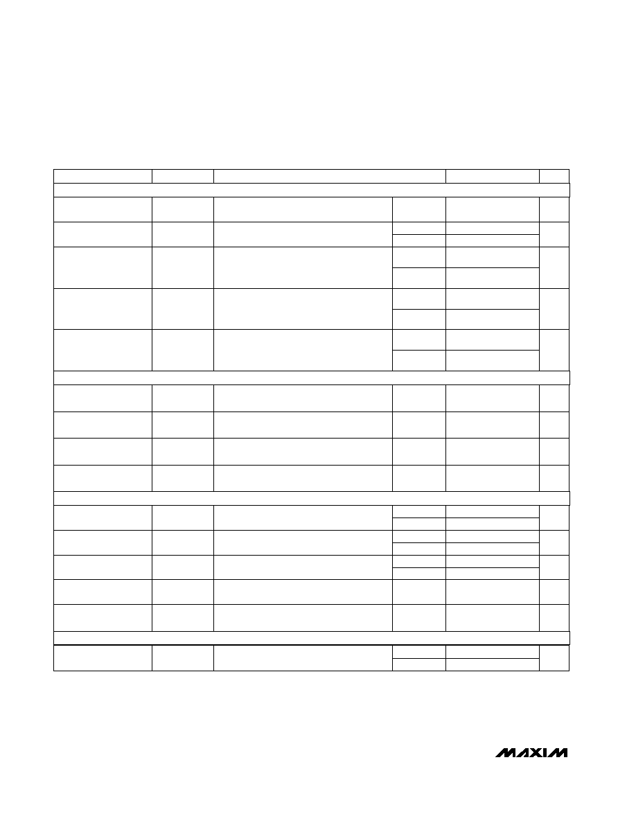
ELECTRICAL CHARACTERISTICS--Single +3.3V Supply
(V
CC
= +3V to +3.6V, V
_H
= 2.0V, V
_L
= 0.5V, T
A
= T
MIN
to T
MAX
, unless otherwise noted. Typical values are at T
A
= +25°C.) (Note 2)
C, E
0
V
CC
V
V
X_
, V
Y_
, V
Z_
,
V
X
, V
Y
, V
Z
Analog-Signal Range
CONDITIONS
MIN
TYP
MAX UNITS
C, E
25
8
20
V
CC
= 3V; I
X
, I
Y
, I
Z
= 10mA;
V
X
, V
Y
, V
Z
= 1.5V
SYMBOL
T
A
= +25°C
R
ON
PARAMETER
Switch On-Resistance
-1
0.0003
1
V
A
, V
B
, V
C
= V
ENABLE
= 0
µA
I
AL
, I
BL
, I
CL
,
I
ENABLEL
Input Current Low
C, E
9
20
V
X_
, V
Y_
, V
Z_
= 1.5V; R
L
= 300
;
C
L
= 35pF; Figure 3
ns
t
ON
Enable Turn-On Time
(Note 6)
T
A
= +25°C
0.5
V
V
AL
, V
BL
, V
CL
,
V
ENABLEL
Input Voltage Low
C, E
-1
0.0003
1
V
A
, V
B
, V
C
= V
ENABLE
= V
CC
µA
I
AH
, I
BH
, I
CH
,
I
ENABLEH
Input Current High
C, E
2.0
V
V
AH
, V
BH
, V
CH
,
V
ENABLEH
Input Voltage High
C, E
25
C, E
0.2
1.5
V
X_
, V
Y_
, V
Z_
= 1.5V; R
L
= 300
; C
L
= 35pF
ns
t
BBM
Break-Before-Make Time
(Note 6)
T
A
= +25°C
6
15
V
X_
, V
Y_
, V
Z_
= 1.5V; R
L
= 300
;
C
L
= 35pF; Figure 3
ns
t
OFF
Enable Turn-Off Time
(Note 6)
T
A
= +25°C
20
C, E
9
20
V
X_
, V
Y_
, V
Z_
= 1.5V/0; R
L
= 300
;
C
L
= 35pF; Figure 2
ns
t
TRANS
Address Transition
Time (Note 6)
T
A
= +25°C
25
C, E
3
C = 1nF, R
S
= 0, V
S
= 0, Figure 5
pC
Q
Charge Injection
(Note 6)
T
A
= +25°C
C, E
-10
10
-1
0.002
1
V
CC
= 3.6V; V
X_
, V
Y_
, V
Z_
= 1V, 3V;
V
X
, V
Y
, V
Z
= 3V, 1V
nA
T
A
= +25°C
I
X_(OFF)
,
I
Y_(OFF)
,
I
Z_(OFF)
X_, Y_, Z_ Off-Leakage
Current (Note 5)
C, E
-10
10
-1
0.002
1
V
CC
= 3.6V; V
X_
, V
Y_
, V
Z_
= 1V, 3V;
V
X
, V
Y
, V
Z
= 3V, 1V
nA
T
A
= +25°C
I
X(OFF)
,
I
Y(OFF)
,
I
Z(OFF)
X, Y, Z Off-Leakage
Current (Note 6)
C, E
-10
10
-1
0.002
1
V
CC
= 3.6V; V
X
, V
Y
, V
Z
= 3V, 1V;
V
X_
, V
Y_
, V
Z_
= 3V, 1V, or floating
nA
T
A
= +25°C
I
X(ON)
,
I
Y(ON)
,
I
Z(ON)
X, Y, Z On-Leakage
Current (Note 6)
1
V
CC
= 3.6V,
V
A
, V
B
, V
C
, V
ENABLE
= V
CC
or 0
µA
I
CC
Power-Supply Current
T
A
= +25°C
10
C, E
ANALOG SWITCH
POWER SUPPLY
SWITCH DYNAMIC CHARACTERISTICS
DIGITAL I/O
MAX4617/MAX4618/MAX4619
High-Speed, Low-Voltage, CMOS Analog
Multiplexers/Switches
_______________________________________________________________________________________
5
Note 2:
The algebraic convention is used in this data sheet; the most negative value is shown in the minimum column.
Note 3:
R
ON
= R
ON(MAX)
- R
ON(MIN)
.
Note 4:
Flatness is defined as the difference between the maximum and minimum value of on-resistance as measured over the specified
analog signal ranges; i.e., V
X_
, V
Y_
, V
Z_
= 3V to 0 and 0 to -3V.
Note 5:
Leakage parameters are 100% tested at maximum-rated hot operating temperature, and guaranteed by correlation at T
A
= +25°C.
Note 6:
Guaranteed by design, not production tested.
ELECTRICAL CHARACTERISTICS--Single +2.5V Supply
(V
CC
= +2.5V, T
A
= T
MIN
to T
MAX
, unless otherwise noted. Typical values are at T
A
= +25°C.) (Note 2)
CONDITIONS
MIN
TYP
MAX UNITS
SYMBOL
PARAMETER
C, E
100
30
60
V
CC
= 2.5V; I
X
, I
Y
, I
Z
= 10mA;
V
X
, V
Y
, V
Z
= 1.2V
T
A
= +25°C
R
ON
Switch On-Resistance
12
V
X_
, V
Y_
, V
Z_
= 1V; R
L
= 300
;
C
L
= 35pF; Figure 3
ns
T
A
= +25°C
t
ON
Enable Turn-On Time
(Note 6)
10
V
X_
, V
Y_
, V
Z_
= 1V; R
L
= 300
;
C
L
= 35pF; Figure 3
ns
T
A
= +25°C
t
OFF
Enable Turn-Off Time
(Note 6)
12
V
X_
, V
Y_
, V
Z_
= 1V; R
L
= 300
;
C
L
= 35pF; Figure 3
ns
T
A
= +25°C
t
TRANS
Address Transition
Time (Note 6)
SWITCH DYNAMIC CHARACTERISTICS
ANALOG SWITCH