________________General Description
The MAX4675/MAX4676 single analog switches feature
3
(max) on-resistance (R
ON
) and 0.7
flatness when
operating from dual ±5V supplies. These switches can
handle Rail-to-Rail
Æ
analog signals. Off-leakage current
is 0.1nA at T
A
= +25∞C. The MAX4675/MAX4676 are
ideal in low-distortion applications and are the pre-
ferred solution over mechanical relays in automated
test equipment or applications where current switching
is required. They are more reliable than mechanical
relays, have low power requirements (<1µA), and are
available in a space-saving 6-pin SOT23 package.
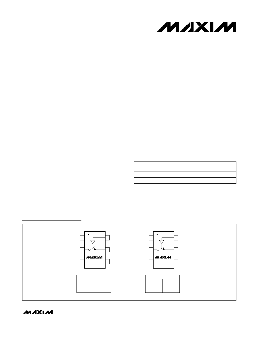
The MAX4675 has a single normally open (NO) switch,
and the MAX4676 has a single normally closed (NC)
switch.
The MAX4675/MAX4676 operate from either a single
+2.7V to +5.5V or dual ±2.7V to ±5.5V supplies, mak-
ing them ideal for use in digital card applications and
single-ended 75
systems.
________________________Applications
Reed Relay Replacement
Test Equipment
Communications Systems
PBX, PABX Systems
Audio Signal Routing
Avionics
ADC Systems
Data-Acquisition Systems
____________________________Features
o 3 (max) R
ON
o 0.7 (max) R
ON
Flatness
o Dual ±2.7V to ±5.5V or Single +2.7V to +5.5V
Supply Range
o Off-Isolation
-75dB at 1MHz, Dual Supply
-65dB at 1MHz, Single Supply
o -3dB Bandwidth 250MHz
o Rail-to-Rail Signal Handling
MAX4675/MAX4676
3
Single SPST Analog Switches
________________________________________________________________ Maxim Integrated Products
1
19-1747; Rev 0; 7/00
For free samples and the latest literature, visit www.maxim-ic.com or phone 1-800-998-8800.
For small orders, phone 1-800-835-8769.
_______________Ordering Information
Rail-to-Rail is a registered trademark of Nippon Motorola, Ltd.
PART
TEMP.
RANGE
PIN-
PACKAGE
SOT
MARK
MAX4675EUT-T
-40
∞C to +85∞C
6 SOT23-6
AAND
MAX4676EUT-T
-40
∞C to +85∞C
6 SOT23-6
AANE
TOP VIEW
MAX4675
IN
SWITCH
0
1
OFF
ON
COM
GND
V-
1
6
IN
5
NO
V+
MAX4675
SOT23
2
3
4
MAX4676
IN
SWITCH
0
1
ON
OFF
COM
GND
V-
1
6
IN
5
NC
V+
MAX4676
SOT23
2
3
4
Pin Configurations/Functional Diagrams/Truth Tables
MAX4675/MAX4676
3
Single SPST Analog Switches
2
_______________________________________________________________________________________
ABSOLUTE MAXIMUM RATINGS
ELECTRICAL CHARACTERISTICS--DUAL SUPPLIES
(V+ = +5V ±10%, V- = -5V ±10%, GND = 0, V
IH
= +2.4V, V
IL
= 0.8V, T
A
= T
MIN
to T
MAX
, unless otherwise noted. Typical values are
at T
A
= +25∞C.) (Notes 2, 3)
Stresses beyond those listed under "Absolute Maximum Ratings" may cause permanent damage to the device. These are stress ratings only, and functional
operation of the device at these or any other conditions beyond those indicated in the operational sections of the specifications is not implied. Exposure to
absolute maximum rating conditions for extended periods may affect device reliability.
V+ to GND ................................................................-0.3V to +6V
V- to GND .................................................................+0.3V to -6V
V+ to V- ..................................................................................12V
IN to GND .....................................................-0.3V to (V+ + 0.3V)
All Other Pins (Note 1) ..........................(V- - 0.3V) to (V+ + 0.3V)
Continuous Current (NO, NC, COM) ..............................±100mA
Peak Current (NO, NC, COM, pulsed at 1ms
(10% duty cycle).........................................................±200mA
Continuous Power Dissipation (T
A
= +70∞C)
6-Pin SOT23 (derate 8.7mW/∞C above +70∞C)............691mW
Operating Temperature Range ...........................-40∞C to +85∞C
Junction Temperature ......................................................+150∞C
Storage Temperature Range .............................-65∞C to +150∞C
Lead Temperature (soldering, 10s) .................................+300∞C
Note 1: Signals on NO, NC, COM, or IN exceeding V+ or V- will be clamped by internal diodes. Limit forward diode current to maxi-
mum current rating.
PARAMETER
SYMBOL
CONDITIONS
MIN
TYP
MAX
UNITS
ANALOG SWITCH
Input Voltage Range
V
COM
,
V
NO,
V
NC
V-
V+
V
T
A
= +25
∞C
2.4
3
On-Resistance
R
ON
V+ = 4.5V, V- = -4.5V, I
COM
= 50mA; V
NO
or V
NC
=
±3.3V
T
A
= T
MIN
to T
MAX
4
T
A
= +25
∞C
0.4
0.7
On-Resistance Flatness
(Note 4)
R
FLAT
V + = 4.5V , V - = - 4.5V ,
I
C OM
= 50m A; V
N O
or
V
N C
=
± 3.3V , 0
T
A
= T
MIN
to T
MAX
1.0
T
A
= +25
∞C
-1
0.1
1
NC or NO Off-Leakage
Current
I
N_(OFF)
V+ = 5.5V, V- = -5.5V,
V
COM
= 4.5V; V
NO
or V
NC
=
±4.5V
T
A
= T
MIN
to T
MAX
-10
10
nA
T
A
= +25
∞C
-1
0.1
1
COM Off-Leakage Current
I
COM(OFF)
V+ = 5.5V, V- = -5.5V,
V
COM
= +4.5V; V
NO
or
V
NC
=
±4.5V
T
A
= T
MIN
to T
MAX
-10
10
nA
T
A
= +25
∞C
-2
0.1
2
COM On-Leakage Current
I
COM(ON)
V+ = 5.5V, V- = -5.5V,
V
COM
=
±4.5V; V
NO
or V
NC
=
± 4.5V or floating
T
A
= T
MIN
to T
MAX
-20
20
nA
LOGIC INPUT
Input Low Voltage
V
IL
0.8
V
Input High Voltage
V
IH
2.4
V
Input Leakage Current
I
IN
-1
0.005
1
µA
DYNAMIC
T
A
= +25
∞C
135
300
Turn-On Time
t
ON
V+ = +4.5V, V- = -4.5V;
V
NO
or V
NC
= 3.3V,
R
L
= 300
, C
L
= 35p F, Fig ure 2
T
A
= T
MIN
to T
MAX
375
ns
T
A
= +25
∞C
50
110
Turn-Off Time
t
OFF
V+ = +4.5V, V- = -4.5V;
V
NO
or V
NC
= 3.3V,
R
L
= 300
, C
L
= 35p F, Fig ure 2
T
A
= T
MIN
to T
MAX
125
ns
MAX4675/MAX4676
3
Single SPST Analog Switches
_______________________________________________________________________________________
3
ELECTRICAL CHARACTERISTICS--DUAL SUPPLIES (continued)
(V+ = +5V ±10%, V- = -5V ±10%, GND = 0, V
IH
= +2.4V, V
IL
= 0.8V, T
A
= T
MIN
to T
MAX
, unless otherwise noted. Typical values are
at T
A
= +25∞C.) (Notes 2, 3)
ELECTRICAL CHARACTERISTICS--SINGLE SUPPLY
(V+ = +5V ±10%, V- = 0, GND = 0, V
IH
= +2.4V, V
IL
= 0.8V, T
A
= T
MIN
to T
MAX
, unless otherwise noted. Typical values are at
T
A
= +25∞C.) (Notes 2, 3)
PARAMETER
SYMBOL
CONDITIONS
MIN
TYP
MAX
UNITS
ANALOG SWITCH
Input Voltage Range
V
COM
,
V
NO,
V
NC
0
V+
V
T
A
= +25
∞C
3.5
5.75
On-Resistance
R
ON
V + = 4.5V ; I
C OM
= 50m A;
V
NO
or V
NC
= 3.3V
T
A
= T
MIN
to T
MAX
7.5
T
A
= +25
∞C
0.4
1.6
On-Resistance Flatness
(Note 4)
R
FLAT
V + = 4.5V ; I
C OM
= 50m A;
V
N O
or V
N C
= 1.5V , 2.5V ,
3.3V
T
A
= T
MIN
to T
MAX
2
T
A
= +25
∞C
-1
0.1
1
NC or NO Off-Leakage
Current
I
N_(OFF)
V+ = 5.5V; V
NO
or
V
NC
= 4.5V or 0;
V
COM
= 0 or 4.5V
T
A
= T
MIN
to T
MAX
-10
10
nA
T
A
= +25
∞C
-1
0.1
1
COM Off-Leakage Current
I
COM(OFF)
V+ = 5.5V; V
NO
or
V
NC
= 4.5V or 0;
V
COM
= 0 or 4.5V
T
A
= T
MIN
to T
MAX
-10
10
nA
PARAMETER
SYMBOL
CONDITIONS
MIN
TYP
MAX
UNITS
Charge Injection
Q
R
GEN
= 0
, C
L
= 1nF,
V
GEN
= 0, Figure 3
T
A
= +25
∞C
87
pC
Off-Isolation
V
ISO
R
L
= 50
, C
L
= 5pF,
f = 1MHz, Figure 4
T
A
= +25
∞C
-75
dB
On-Channel Bandwidth
(-3dB)
BW
R
S
= 50
, R
L
= 50
250
MHz
NC or NO Off-Capacitance
C
(N_OFF)
f = 1MHz, Figure 5
T
A
= +25
∞C
85
pF
COM Off-Capacitance
C
( C OM OFF)
f = 1MHz, Figure 5
T
A
= +25
∞C
85
pF
On-Capacitance
C
(ON)
f = 1MHz, Figure 5
T
A
= +25
∞C
350
pF
POWER SUPPLY
Supply Voltage
V+, V-
±2.7
±5.5
V
T
A
= +25
∞C
0.002
1
Positive Supply Current
I+
V
IN
= 0 or 5.5V, V+ =
5.5V, V- = -5.5V
T
A
= T
MIN
to T
MAX
10
µA
T
A
= +25
∞C
-1
-0.002
Negative Supply Current
I-
V
IN
= 0 or 5.5V,
V+ = 5.5V, V- = -5.5V
T
A
= T
MIN
to T
MAX
-10
µA
MAX4675/MAX4676
3
Single SPST Analog Switches
4
_______________________________________________________________________________________
Note 2: Parameters are 100% tested at +25
∞C only and guaranteed by correlation through the full-rated temperature range.
Note 3: The algebraic convention, where the most negative value is a minimum and the most positive value a maximum, is used in
this data sheet.
Note 4: Flatness is defined as the difference between the maximum and minimum value of R
ON
as measured over the specified
analog signal ranges.
PARAMETER
SYMBOL
CONDITIONS
MIN
TYP
MAX
UNITS
T
A
= +25
∞C
-2
0.2
2
COM On-Leakage Current
I
COM (ON)
V+ = 5.5V; V
NO
or
V
NC
= 0, 4.5V,
or floating;
V
COM
= 0 or 4.5V
T
A
= T
MIN
to T
MAX
-20
20
nA
LOGIC INPUT
Input Low Voltage
V
IL
0.8
V
Input High Voltage
V
IH
2.4
V
Input Leakage Current
I
IN
-1
0.005
1
µA
DYNAMIC
T
A
= +25
∞C
350
700
Turn-On Time
t
ON
V + = + 4.5V ;
V
NO
or V
NC
= +3.3V,
R
L
= 300
, C
L
= 35p F,
Fi gur e 2
T
A
= T
MIN
to
T
MAX
850
ns
T
A
= +25
∞C
55
150
Turn-Off Time
t
OFF
V+ = +4.5V; V
NO
or V
NC
=
+3.3V, R
L
= 300
,
C
L
= 35pF, Figure 2
T
A
= T
MIN
to
T
MAX
160
ns
Charge Injection
Q
R
GEN
= 0
, C
L
= 1nF,
V
GEN
= 2.5V, Figure 3
T
A
= +25
∞C
31
pC
Off-Isolation
V
ISO
R
L
= 50
, C
L
= 5pF,
f = 1MHz, Figure 4
T
A
= +25
∞C
-65
dB
On-Channel Bandwidth
(-3dB)
R
S
= 50
, R
L
= 50
150
MHz
NC or NO Off-Capacitance
C
(N_OFF)
f = 1MHz, Figure 5
T
A
= +25
∞C
85
pF
COM Off-Capacitance
C
( C OM OFF)
f = 1MHz, Figure 5
T
A
= +25
∞C
85
pF
On-Capacitance
C
(ON)
f = 1MHz, Figure 5
T
A
= +25
∞C
350
pF
POWER SUPPLY
Supply Voltage
V+
2.7
5.5
V
T
A
= +25
∞C
0.002
1
Positive Supply Current
I+
V
IN
= 0 or 5V,
V+ = 5.5V
T
A
= T
MIN
to T
MAX
10
µA
ELECTRICAL CHARACTERISTICS--SINGLE SUPPLY (continued)
(V+ = +5V ±10%, V- = 0, GND = 0, V
IH
= +2.4V, V
IL
= 0.8V, T
A
= T
MIN
to T
MAX
, unless otherwise noted. Typical values are at
T
A
= +25∞C.) (Notes 2, 3)
MAX4675/MAX4676
3
Single SPST Analog Switches
_______________________________________________________________________________________
5
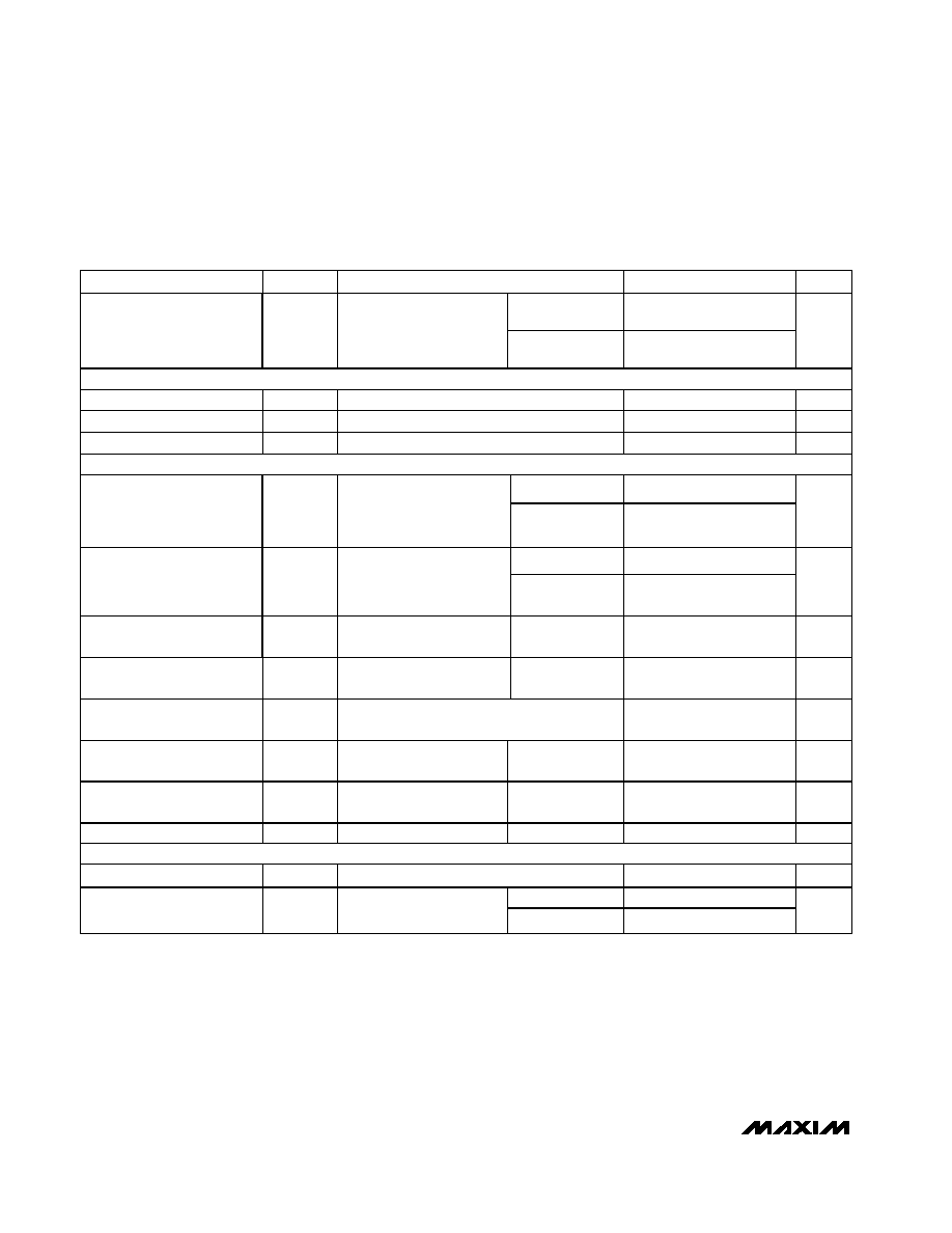
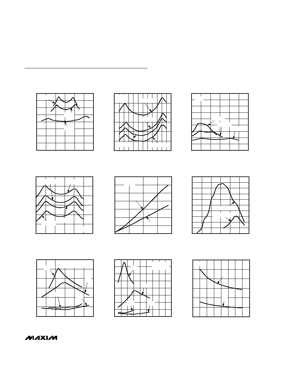
Typical Operating Characteristics
(T
A
= +25∞C, unless otherwise noted.)
0
0.5
1.0
1.5
2.0
2.5
3.0
3.5
4.0
-6
-2
-4
0
2
4
6
ON-RESISTANCE
vs. V
COM
(DUAL SUPPLIES)
MAX4675 toc01
V
COM
(V)
R
ON
(
)
V =
±3V
V =
±2.5V
V =
±5V
1.5
1.9
1.7
2.3
2.1
2.5
2.7
-6
-4 -3 -2
-5
-1
1
0
2
3
4
5
6
ON-RESISTANCE vs. V
COM
AND TEMPERATURE (DUAL SUPPLIES)
MAX4675 toc02
V
COM
(V)
R
ON
(
)
V+ = 5V
V- = -5V
T
A
= +25
∞C
T
A
= +85
∞C
T
A
= -40
∞C
T
A
= 0
∞C
0
4
2
10
8
6
16
14
12
18
0
2
1
3
4
5
6
ON-RESISTANCE
vs. V
COM
(SINGLE SUPPLY)
MAX4675 toc03
V
COM
(V)
R
ON
(
)
V- = 0
V+ = +2.7V
V+ = +3.3V
V+ = +5V
2.0
3.0
2.5
4.0
3.5
4.5
5.0
0
2
3
1
4
5
6
ON-RESISTANCE vs. V
COM
AND TEMPERATURE (SINGLE SUPPLY)
MAX4675 toc04
V
COM
(V)
R
ON
(
)
V+ = +5V
T
A
= +25
∞C
T
A
= +85
∞C
T
A
= -40
∞C
T
A
= 0
∞C
0
4
2
8
6
10
12
14
ON/OFF-LEAKAGE CURRENT
vs. TEMPERATURE
MAX4675 toc05
TEMPERATURE (
∞C)
ON/OFF-LEAKAGE CURRENT (nA)
50
90
70
110
130
I
COM(ON)
I
COM(OFF)
V+ = 5V
V- = -5V
0
30
20
10
40
50
60
70
80
90
100
-6
-2
-4
0
2
4
6
CHARGE INJECTION
vs. V
COM
MAX4675 toc06
V
COM
(V)
Q (pC)
DUAL SUPPLIES
SINGLE SUPPLY
0
150
100
50
200
250
300
-6
-2
-4
0
2
4
6
TURN-ON/TURN-OFF TIMES
vs. V
COM
(DUAL SUPPLIES)
MAX4675 toc07
V
COM
(V)
t
ON
, t
OFF
(ns)
A: V+ = +3.5V, V- = -3.5V
B: V+ = +5V, V- = -5V
t
OFFA
t
OFFB
t
ONA
t
ONB
0
200
100
500
400
300
700
600
800
0
3
4
1
2
5
6
7
8
9
TURN-ON/TURN-OFF TIMES vs. V
COM
(SINGLE SUPPLY)
MAX4675 toc08
V
COM
(V)
t
ON
, t
OFF
(ns)
A: V+ = +5.5V
B: V+ = +3V
t
OFFA
t
OFFB
t
ONA
t
ONB
0
50
100
150
200
250
300
2.0
3.0
2.5
3.5
4.0
4.5
5.0
5.5
6.0
TURN-ON/TURN-OFF TIMES
vs. SUPPLY VOLTAGE (DUAL SUPPLIES)
MAX4675 toc09
SUPPLY VOLTAGE (V+, V-)
t
ON
, t
OFF
(ns)
V+ = IV-|
t
OFF
t
ON