Äîêóìåíòàöèÿ è îïèñàíèÿ www.docs.chipfind.ru
General Description
The MAX4691MAX4694 are low-voltage CMOS analog
ICs configured as an 8-channel multiplexer (MAX4691),
two 4-channel multiplexers (MAX4692), three single-
pole/double-throw (SPDT) switches (MAX4693), and
four SPDT switches (MAX4694).
The MAX4691/MAX4692/MAX4693 operate from either
a single +2V to +11V power supply or dual ±2V to
±5.5V power supplies. When operating from ±5V sup-
plies they offer 25
on-resistance (R
ON
), 3.5
(max)
R
ON
flatness, and 3
(max) matching between chan-
nels. The MAX4694 operates from a single +2V to +11V
supply. Each switch has Rail-to-Rail
®
signal handling
and a low 1nA leakage current.
All digital inputs are 1.8V logic-compatible when oper-
ating from a +3V supply and TTL compatible when
operating from a +5V supply.
The MAX4691MAX4694 are available in 16-pin,
4mm
4mm QFN and 16-bump UCSP packages. The
chip-scale package (UCSPTM) occupies a 2mm x 2mm
area, significantly reducing the required PC board area.
Applications
Audio and Video Signal Routing
Cellular Phones
Battery-Operated Equipment
Communications Circuits
Modems
Features
o 16 bump, 0.5mm-Pitch UCSP (2mm x 2mm)
o 1.8V Logic Compatibility
o Guaranteed On-Resistance
70
(max) with +2.7V Supply
35
(max) with +5V Supply
25
(max) with ±4.5V Dual Supplies
o Guaranteed Match Between Channels
5
(max) with +2.7V Supply
3
(max) with ±4.5V Dual Supplies
o Guaranteed Flatness Over Signal Range
3.5
(max) with ±4.5V Dual Supplies
o Low Leakage Currents Over Temperature
20nA (max) at +85°C
o Fast 90ns Transition Time
o Guaranteed Break-Before-Make
o Single-Supply Operation from +2V to +11V
o Dual-Supply Operation from ±2V to ±5.5V
(MAX4691/MAX4692/MAX4693)
o V+ to V- Signal Handling
o Low Crosstalk: -90dB (100kHz)
o High Off-Isolation: -88dB (100kHz)
MAX4691MAX4694
Low-Voltage 8:1 Mux/Dual 4:1 Mux/Triple SPDT/
Quad SPDT in UCSP Package
________________________________________________________________ Maxim Integrated Products
1
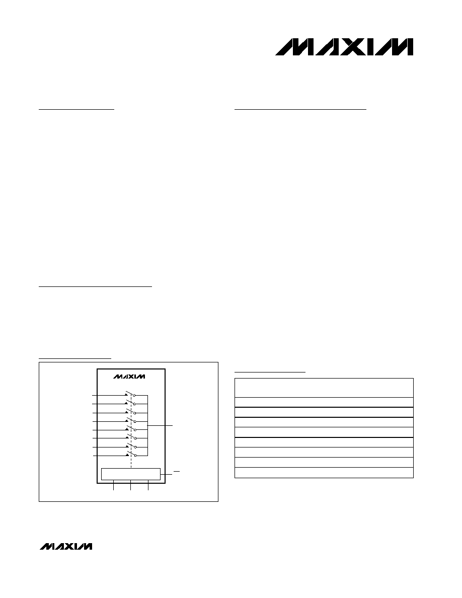
Functional Diagrams
19-1945; Rev 2; 2/03
Pin Configurations appear at end of data sheet.
Functional Diagrams continued at end of data sheet.
Rail-to-Rail is a registered trademark of Nippon Motorola, Ltd.
UCSP is a trademark of Maxim Integrated Products, Inc.
PART
TEMP
RANGE
PIN-
PACKAGE
MAX4691EBE-T
-40
°C to +85°C
16-Bump UCSP*
MAX4691EGE
-40
°C to +85°C
16 QFN
MAX4692EBE-T
-40
°C to +85°C
16-Bump UCSP*
MAX4692EGE
-40
°C to +85°C
16 QFN
MAX4693EBE-T
-40
°C to +85°C
16-Bump UCSP*
MAX4693EGE
-40
°C to +85°C
16 QFN
MAX4694EBE-T
-40
°C to +85°C
16-Bump UCSP*
MAX4694EGE
-40
°C to +85°C
16 QFN
Ordering Information
*Requires special solder temperature profile described in the
Absolute Maximum Ratings section.
*UCSP reliability is integrally linked to the user's assembly meth-
ods, circuit board, and environment. See the UCSP Reliability
Notice in the UCSP Reliability section for information.
MAX4691
X0
X1
X2
X3
X4
X5
X6
X7
LOGIC
C
B
A
EN
X
For pricing, delivery, and ordering information, please contact Maxim/Dallas Direct! at
1-888-629-4642, or visit Maxim's website at www.maxim-ic.com.
MAX4691MAX4694
Low-Voltage 8:1 Mux/Dual 4:1 Mux/Triple SPDT/
Quad SPDT in UCSP Package
2
_______________________________________________________________________________________
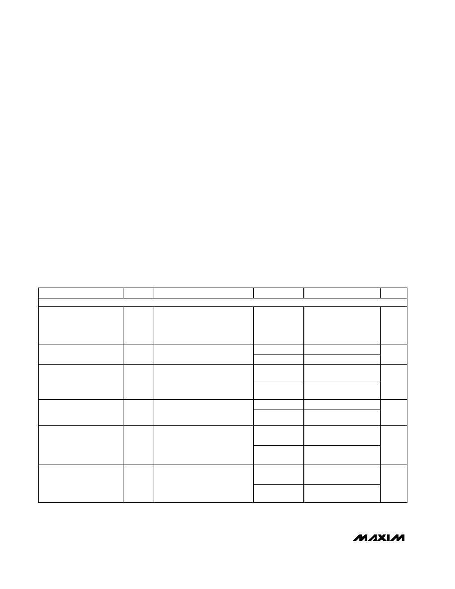
ABSOLUTE MAXIMUM RATINGS
ELECTRICAL CHARACTERISTICS--Single +3V Supply
(V+ = +2.7V to +3.6V, V- = 0, V
IH
= +1.4V, V
IL
= +0.4V, T
A
= -40°C to +85°C, unless otherwise noted. Typical values are at
T
A
= +25°C.) (Notes 3, 4, 5)
Stresses beyond those listed under "Absolute Maximum Ratings" may cause permanent damage to the device. These are stress ratings only, and functional
operation of the device at these or any other conditions beyond those indicated in the operational sections of the specifications is not implied. Exposure to
absolute maximum rating conditions for extended periods may affect device reliability.
V+ to GND ..............................................................-0.3V to +12V
V+ to V- (MAX4691/MAX4692/MAX4693) ..............-0.3V to +12V
Voltage into any Terminal (Note 1) ...... (V- - 0.3V) to (V+ + 0.3V)
Continuous Current into any Terminal ............................. ±20mA
Peak Current W_, X_, Y_, Z_ (pulsed at 1ms,
10% duty cycle)...........................................................±40mA
ESD per Method 3015.7.......................................................>2kV
Continuous Power Dissipation (T
A
= +70°C)
16-Bump UCSP (derate 8.3mW/°C above +70°C) .... 659mW
16-Pin QFN (derate 18.5mW/°C above +70°C) ....... 1481mW
Operating Temperature Range .......................... -40°C to +85°C
Storage Temperature Range ............................ -65°C to +150°C
Lead Temperature (Soldering)
16-Bump UCSP (Note 2) Infrared (15s) ..................... +220°C
Vapor Phase (60s)..................................................... +215°C
16-Pin QFN................................................................. +300°C
Note 1: Voltages exceeding V+ or V- on any signal terminal are clamped by internal diodes. Limit forward-diode current to maxi-
mum current rating.
Note 2: This device is constructed using a unique set of packaging techniques that impose a limit on the thermal profile the device
can be exposed to during board level solder attach and rework. This limit permits only the use of the solder profiles recom-
mended in the industry standard specification, JEDEC 020A, paragraph 7.6, Table 3 for IR/VPR and convection reflow.
Preheating is required. Hand or wave soldering is not allowed.
PARAMETER
SYMBOL
CONDITIONS
T
A
MIN
TYP
MAX
UNITS
ANALOG SWITCH
Analog Signal Range
V
W
, V
X
, V
Y
,
V
Z
,
V
W
_,
V
X
_, V
Y
_,
V
Z
_
- 40°C to + 85°C
0
V+
V
+ 25ºC 45
70
On-Resistance (Note 6)
R
ON
V+ = 2.7V; I
W
, I
X
, I
Y
, I
Z
= 1mA
V
W
_, V
X
_, V
Y
_, V
Z
_ = 1.5V
- 40°C to + 85°C
80
+ 25°C 2
5
On-Resistance Match
Between Channels
(Notes 6, 7)
R
ON
V+ = 2.7V; I
W
, I
X
, I
Y
, I
Z
= 1mA
V
W
_, V
X
_, V
Y
_, V
Z
_ = 1.5V
- 40°C to + 85°C
6
+ 25°C -1
1
W_, X_, Y_, Z_ Off-Leakage
Current (Note 9)
I
W
_, I
X
_,
I
Y
_, I
Z
_
V+ = 3.6V; V
W
,
V
X
, V
Y
, V
Z
= 3V,
0.6V; V
W
_, V
X
_, V
Y
_, V
Z
_ = 0.6V,
3V
- 40°C to + 85°C -10
10
nA
+ 25°C -2
2
W, X, Y, Z Off-Leakage
Current (Note 9)
I
W(OFF)
,
I
X(OFF)
,
I
Y(OFF)
,
I
Z(OFF)
V+ = 3.6V; V
W
,
V
X
, V
Y
, V
Z
= 3V,
0.6V; V
W
_, V
X
_, V
Y
_, V
Z
_ = 0.6V,
3V
- 40°C to + 85°C -20
20
nA
+ 25°C -2
2
W, X, Y, Z On-Leakage
Current (Note 9)
I
W(ON)
,
I
X(ON)
,
I
Y(ON)
,
I
Z(ON)
V+ = 3.6V; V
W
,
V
X
, V
Y
, V
Z
= 0.6V,
3V; V
W
_, V
X
_, V
Y
_, V
Z
_ = 0.6V, 3V,
or floating
- 40°C to + 85°C -20
20
nA
MAX4691MAX4694
Low-Voltage 8:1 Mux/Dual 4:1 Mux/Triple SPDT/
Quad SPDT in UCSP Package
_______________________________________________________________________________________
3
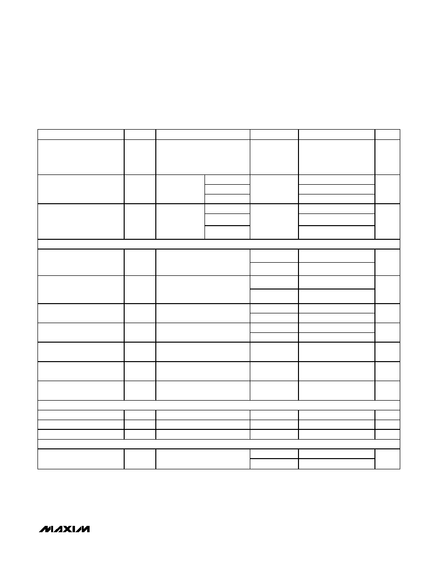
ELECTRICAL CHARACTERISTICS--Single +3V Supply (continued)
(V+ = +2.7V to +3.6V, V- = 0, V
IH
= +1.4V, V
IL
= +0.4V, T
A
= -40°C to +85°C, unless otherwise noted. Typical values are at
T
A
= +25°C.) (Notes 3, 4, 5)
PARAMETER
SYMBOL
CONDITIONS
T
A
MIN
TYP
MAX
UNITS
Input Off-Capacitance
C
W
_
(OFF)
,
C
X
_
(OFF)
,
C
Y
_
(OFF)
,
C
Z
_
(OFF)
f = 1MHz, Figure 7
+ 25°C 9
pF
MAX4691
68
MAX4692
36
Output Off-Capacitance
C
X(OFF)
,
C
Y(OFF)
,
C
Z(OFF)
f = 1MHz,
Figure 7
MAX4693
+ 25°C
20
pF
MAX4691
78
MAX4692
46
On-Capacitance
C
W(ON)
,
C
X(ON)
,
C
Y(ON)
,
C
Z(ON)
f = 1MHz,
Figure 7
MAX4693
+ 25°C
30
pF
DYNAMIC
+ 25°C 180
300
Enable Turn-On Time
( M AX 4691/M AX 4692/
M AX 4693)
t
ON
V
W
_, V
X
_, V
Y
_, V
Z
_ = 1.5V;
R
L
= 300
,C
L
= 35pF, Figure 2
- 40°C to + 85°C
350
ns
+ 25°C 70
100
Enable Turn-Off Time
( M AX 4691/M AX 4692/
M AX 4693)
t
OFF
V
W
_, V
X
_, V
Y
_, V
Z
_ = 1.5V;
R
L
= 300
,C
L
= 35pF, Figure 2
- 40°C to + 85°C
120
ns
+ 25°C 200
350
Address Transition Time
t
TRANS
V
W
_, V
X
_, V
Y
_, V
Z
_ = 0, 1.5V;
R
L
= 300
, C
L
= 35pF, Figure 3
- 40°C to + 85°C
400
ns
+ 25°C 2
90
Break-Before-Make
t
BBM
V
W
_, V
X
_, V
Y
_, V
Z
_ = 1.5V;
R
L
= 300
, C
L
= 35pF, Figure 4
- 40°C to + 85°C
2
ns
Charge Injection
Q
V
GE N
= 0; R
GE N
= 0; C
L
= 1nF,
Fi g ur e 5
+ 25°C 0.1
pC
Off-Isolation (Note 10)
V
ISO
f = 0.1MHz, R
L
= 50
, C
L
= 5pF,
Figure 6
+ 25°C -70
dB
Crosstalk (Note 11)
V
CT
f = 0.1MHz, R
L
= 50
, C
L
= 5pF,
Figure 6
+ 25°C -75
dB
DIGITAL I/O
Input Logic High
V
IH
1.4
V
Input Logic Low
V
IL
0.4
V
Input Leakage Current
I
IN
V
A
,
V
B
, V
C
, V
EN
= 0 or V+
-1
+1
µA
SUPPLY
+ 25°C 0.1
Positive Supply Current
I+
V+ = 3.6V, V
A
, V
B
, V
C
, V
EN
= 0
or V+
- 40°C to + 85°C
1
µA
MAX4691MAX4694
Low-Voltage 8:1 Mux/Dual 4:1 Mux/Triple SPDT/
Quad SPDT in UCSP Package
4
_______________________________________________________________________________________
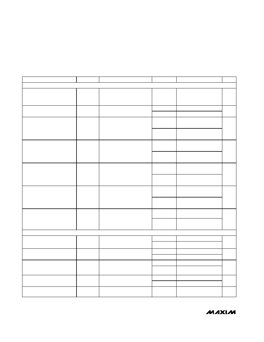
ELECTRICAL CHARACTERISTICS--Single +5V Supply
(V+ = +4.5V to +5.5V, V- = 0, V
IH
= +2V, V
IL
= +0.8V, T
A
= -40°C to +85°C, unless otherwise noted. Typical values are at
T
A
= +25°C.) (Notes 3, 4, 5)
PARAMETER
SYMBOL
CONDITIONS
T
A
MIN
TYP
MAX
UNITS
ANALOG SWITCH
Analog Signal Range
V
W
, V
X
, V
Y
,
V
Z
, V
W
_, V
X
_,
V
Y
_, V
Z
_
_
- 40°C to + 85°C 0
V+
V
+ 25°C 25
35
On-Resistance (Note 6)
R
ON
V+ = 4.5V; I
W
, I
X
, I
Y
, I
Z
= 1mA;
V
W
_,
V
X
_, V
Y
_, V
Z
_ = 3.5V
- 40°C to + 85°C 40
+ 25°C 2
4
On-Resistance Match
Between Channels
(Notes 6, 7)
R
ON
V+ = 4.5V; I
W
, I
X
, I
Y
, I
Z
= 1mA;
V
W
_,
V
X
_, V
Y
_, V
Z
_ = 3.5V
- 40°C to + 85°C 5
+ 25°C 2
6
On-Resistance Flatness
(Note 8)
R
FLAT(ON)
V+ = 4.5V; I
W
, I
X
, I
Y
, I
Z
= 1mA;
V
W
_,
V
X
_, V
Y
_, V
Z
_ = 1V, 2.25V,
3.5V
- 40°C to + 85°C 8
+ 25°C -1
1
W_, X_ , Y_, Z_ Off-Leakage
Current (Note 9)
I
W_
,
I
X _
,
I
Y _
, I
Z _
V+ = 5.5V; V
W
,
V
X
, V
Y
,
V
Z
= 4.5V, 1V_; V
W
_, V
X
_, V
Y
_,
V
Z
_ = 1V, 4.5V
- 40°C to + 85°C -10
10
nA
+ 25°C -2
2
W, X, Y, Z Off-Leakage
Current (Note 9)
I
W(OFF)
,
I
X (OFF)
,
I
Y(OFF)
,
I
Z(OFF)
V+ = 5.5V; V
W
,
V
X
, V
Y
,
V
Z
= 4.5V, 1V_; V
W
_,
V
X
_, V
Y
_,
V
Z
_ = 1V, 4.5V
- 40°C to + 85°C -20
20
nA
+ 25°C -2
2
W, X, Y, Z On-Leakage
Current (Note 9)
I
W(ON)
,
I
X(ON)
,
I
Y(ON)
,
I
Z(ON)
V + = 5.5V ; V
W
,
V
X
, V
Y
, V
Z
= 1V ,
4.5V _; V
W
_,
V
X
_, V
Y
_, V
Z
_ = 1V,
4.5V , or floating
- 40°C to + 85°C -20
20
nA
DYNAMIC
+ 25°C 90
130
Enable Turn-On Time
( M AX 4691/M AX 4692/M AX 4693)
t
ON
V
W
_,
V
X
_, V
Y
_, V
Z
_ = 3V; R
L
=
300
, C
L
= 35pF, Figure 2
- 40°C to + 85°C 150
ns
+ 25°C 45
60
Enable Turn-Off Time
( M AX 4691/M AX 4692/M AX 4693)
t
OFF
V
W
_,
V
X
_, V
Y
_, V
Z
_ = 3V; R
L
=
300
, C
L
= 35pF, Figure 2
- 40°C to + 85°C 70
ns
+ 25°C 100
140
Ad d r ess Tr ansi ti on Ti m e
t
TRANS
V
W
_,
V
X
_, V
Y
_, V
Z
_ = 0, 3V;
R
L
= 300
, C
L
= 35pF,
Figure 3
- 40°C to + 85°C 160
ns
+ 25°C 2
35
Break-Before-Make
t
BBM
V
W
_,
V
X
_, V
Y
_, V
Z
_ = 3V; R
L
=
300
, C
L
= 35pF, Figure 4
- 40°C to + 85°C 2
ns
Charge Injection
Q
V
GEN
= 0; R
GEN
= 0; C
L
= 1nF,
Figure 5
+ 25°C 0.2
pC
MAX4691MAX4694
Low-Voltage 8:1 Mux/Dual 4:1 Mux/Triple SPDT/
Quad SPDT in UCSP Package
_______________________________________________________________________________________
5
ELECTRICAL CHARACTERISTICS--Dual ±5V Supplies
(MAX4691/MAX4692/MAX4693 only)
(V+ = +4.5V to +5.5V, V- = -4.5V to -5.5V, V
IH
= +2V, V
IL
= +0.8V, T
A
= -40°C to +85°C, unless otherwise noted.) (Notes 3, 4, 5)
PARAMETER
SYMBOL
CONDITIONS
T
A
MIN
TYP
MAX
UNITS
ANALOG SWITCH
Analog Signal Range
V
X
, V
Y
, V
Z
,
V
X
_, V
Y
_, V
Z
_
- 40°C to + 85°C V-
V+
V
+ 25°C 18
25
On-Resistance (Note 6)
R
ON
V+ = 4.5V; I
X
, I
Y
, I
Z
= 10mA;
V- = -4.5V; V
X
_, V
Y
_, V
Z
_ = 3.5V - 40°C to + 85°C 30
+ 25°C 2
3
On-Resistance Match
Between Channels
(Notes 6, 7)
R
ON
V+ = 4.5V; V- = -4.5V; I
X
, I
Y
, I
Z
=
10mA;
V
X
_, V
Y
_, V
Z
_ = 3.5V
- 40°C to + 85°C 4
+ 25°C 2.5
3.5
On-Resistance Flatness
(Note 8)
R
FLAT(ON)
V+ = 4.5V; V- = -4.5V; I
X
, I
Y
, I
Z
=
10mA; V
X
, V
Y
, V
Z
= 3.5V, 0,
-3.5V
- 40°C to + 85°C 4
+ 25°C -1
1
X_ , Y_, Z_ Off-Leakage
Current (Note 9)
I
X
_,
I
Y
_, I
Z
_
V+ = 5.5V; V- = -5.5V; V
X
, V
Y
, V
Z
= +4.5V;
V
X
_, V
Y
_, V
Z
_ =
±4.5V
- 40°C to + 85°C -10
10
nA
+ 25°C -2
2
X, Y, Z Off-Leakage Current
(Note 9)
I
X (OFF)
,
I
Y(OFF)
,
I
Z(OFF)
V+ = 5.5V; V- = -5.5V; V
X
, V
Y
,
V
Z
= +4.5V;
V
X
_, V
Y
_, V
Z
_ =
±4.5V
- 40°C to + 85°C -20
20
nA
ELECTRICAL CHARACTERISTICS--Single +5V Supply (continued)
(V+ = +4.5V to +5.5V, V- = 0, V
IH
= +2V, V
IL
= +0.8V, T
A
= -40°C to +85°C, unless otherwise noted. Typical values are at
T
A
= +25°C.) (Notes 3, 4, 5)
PARAMETER
SYMBOL
CONDITIONS
T
A
MIN
TYP
MAX
UNITS
Off-Isolation (Note 10)
V
ISO
f = 0.1MHz, R
L
= 50
,
C
L
= 5pF, Figure 6
+ 25°C -80
dB
Crosstalk (Note 11)
V
CT
f = 0.1MHz, R
L
= 50
,
C
L
= 5pF, Figure 6
+ 25°C -87
dB
DIGITAL I/O
Input Logic High
V
IH
2
V
Input Logic Low
V
IL
0.8
V
Input Leakage Current
I
IN
V
A
, V
B
, V
C
, V
EN
= 0 or V+
-1
+1
µA
SUPPLY
+ 25°C 0.1
Positive Supply Current
I+
V+ = 5.5V; V
A
, V
B
, V
C
, V
EN
= 0
or V+
- 40°C to + 85°C 1
µA