General Description
The MAX4696/MAX4697/MAX4698 low on-resistance
(R
ON
), low-voltage analog switches operate from a sin-
gle +2.0V to +5.5V supply. The MAX4696/MAX4697 are
single-pole/single-throw (SPST) analog switches, and
the MAX4698 is a single-pole/double-throw (SPDT) ana-
log switch. The MAX4696 is a normally open (NO)
switch, and the MAX4697 is a normally closed (NC)
switch.
When powered from a 2.7V supply, these devices feature
35
(max) R
ON
, with 2
(max) R
ON
matching and 13
(max) flatness. The MAX4696/MAX4697/MAX4698 offer
fast switching speeds (t
ON
= 80ns max, t
OFF
= 25ns
max). The MAX4698 offers a break-before-make function.
The digital logic inputs are 1.8V logic compatible from a
+2.7V to +3.3V supply and are TTL/CMOS compatible
from a +4.5V to +5.5V supply. The MAX4696/MAX4697/
MAX4698 are packaged in the chip-scale package
(UCSPTM), significantly reducing the required PC board
area. The device occupies only a 1.50mm
1.02mm
area. The 3
2 array of solder bumps are spaced with
a 0.5mm bump pitch.
________________________Applications
MP3 Players
Battery-Operated Equipment
Relay Replacement
Audio and Video Signal Routing
Communications Circuits
PCMCIA Cards
Cellular Phones
Hard Drives
Modems
Features
o 6-Bump, 0.5mm Pitch, UCSP
o R
ON
35
max (+3V Supply)
20
max (+5V Supply)
o 2 max R
ON
Match Between Channels
o 13 max R
ON
Flatness Over Signal Range
o Low Leakage Currents Over Temperature
1nA (max) at T
A
= +25�C
o Fast Switching: t
ON
= 80ns, t
OFF
= 25ns
o Guaranteed Break-Before-Make (MAX4698)
o +2.0V to +5.5V Single-Supply Operation
o Rail-to-Rail
�
Signal Handling
o Low Crosstalk: -75dB (100kHz)
o High Off-Isolation: -75dB (100kHz)
o 1.8V CMOS Logic Compatible
o -3dB Bandwidth: >200MHz
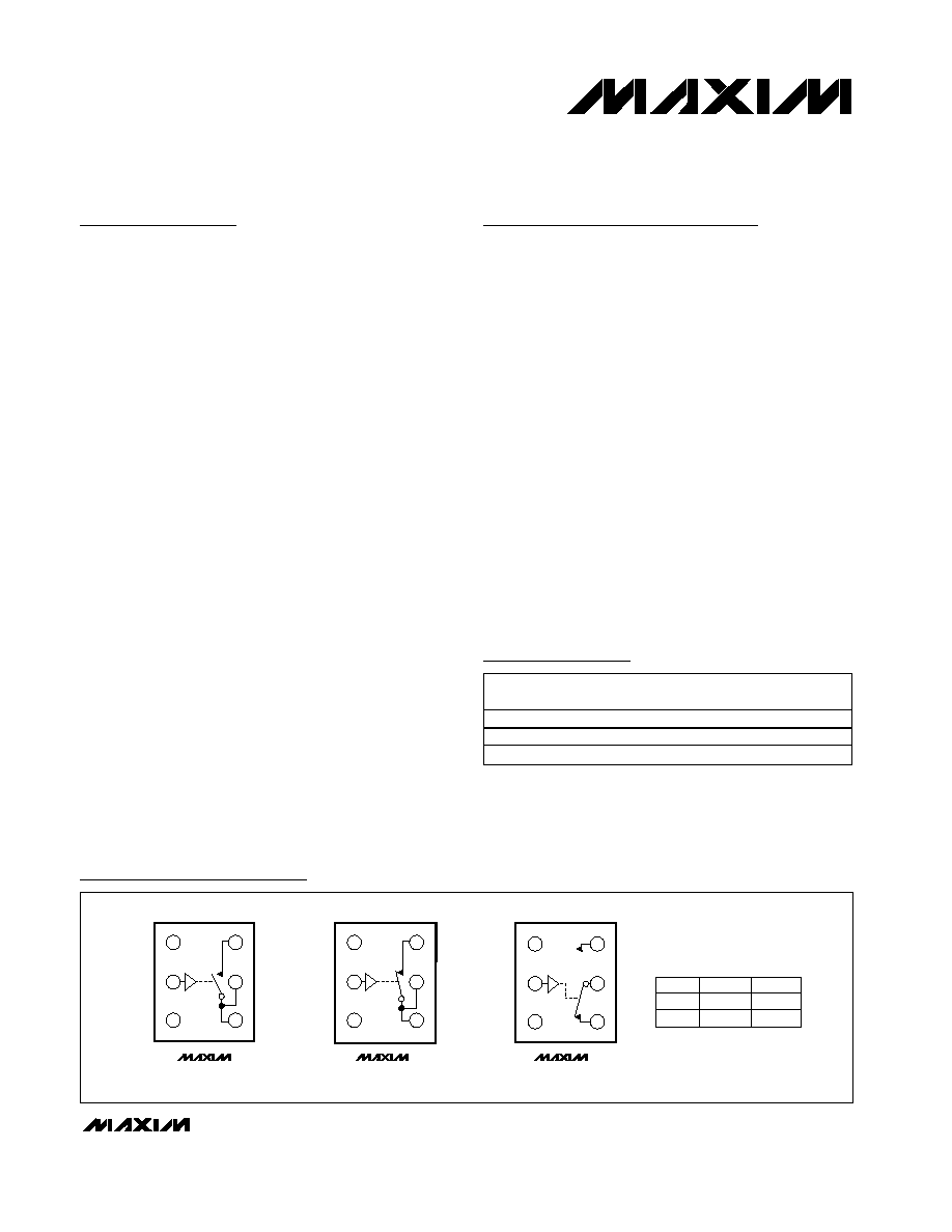
MAX4696/MAX4697/MAX4698
35
, Low-Voltage, SPST/SPDT
Analog Switches in UCSP Package
________________________________________________________________ Maxim Integrated Products
1
IN
COM
GND
NO
V+
TOP VIEW
IN
NC
GND
NO
COM
V+
MAX4698
IN
COM
GND
NC
V+
MAX4697
MAX4696
IN
0
1
NO
OFF
ON
NC
ON
OFF
B3
COM
B1
A3
A2
A1
B2
B3
B1
A3
A2
A1
B2
COM
B3
B1
A3
A2
A1
B2
SWITCHES SHOWN FOR LOGIC "0"
Pin Configurations/Functional Diagrams/Truth Table
19-1994; Rev 3; 2/03
Ordering Information
PART
TEMP
RANGE
PIN/BUMP-
PACKAGE
TOP
MARK
MAX4696EBT-T
-40�C to +85�C
6 UCSP
AAL
MAX4697EBT-T
-40�C to +85�C
6 UCSP
AAM
MAX4698EBT-T
-40�C to +85�C
6 UCSP
AAN
Rail-to-Rail is a registered trademark of Nippon Motorola, Ltd.
UCSP is a trademark of Maxim Integrated Products, Inc.
For pricing, delivery, and ordering information, please contact Maxim/Dallas Direct! at
1-888-629-4642, or visit Maxim's website at www.maxim-ic.com.
MAX4696/MAX4697/MAX4698
35
, Low-Voltage, SPST/SPDT
Analog Switches in UCSP Package
2
_______________________________________________________________________________________
ABSOLUTE MAXIMUM RATINGS
ELECTRICAL CHARACTERISTICS--Single +3V Supply
(V+ = +2.7V to +3.3V, V
IH
= +1.4V, V
IL
= 0.5V, T
A
= T
MIN
to T
MAX
, unless otherwise noted. Typical values are at +3V and
T
A
= +25�C.) (Notes 2, 8)
Stresses beyond those listed under "Absolute Maximum Ratings" may cause permanent damage to the device. These are stress ratings only, and functional
operation of the device at these or any other conditions beyond those indicated in the operational sections of the specifications is not implied. Exposure to
absolute maximum rating conditions for extended periods may affect device reliability.
All Voltages Referenced to GND
V+, IN .......................................................................-0.3V to +6V
COM, NO, NC (Note 1).................................-0.3V to (V+ + 0.3V)
Continuous Current COM, NO, NC ..................................�20mA
Peak Current COM, NO, NC
(pulsed at 1ms, 10% duty cycle) .................................�40mA
Continuous Power Dissipation (T
A
= +70�C)
3
2 UCSP (derate 10.1mW/�C at +70�C)....................808mW
Operating Temperature Range ...........................-40�C to +85�C
Storage Temperature Range .............................-65�C to +150�C
Bump Temperature (soldering)
Infrared (15s) ................................................................+220�C
Vapor Phase (60s) ........................................................+215�C
PARAMETER
SYMBOL
CONDITIONS
T
A
MIN
TYP
MAX
U N I T S
ANALOG SWITCH
Analog Signal Range
V
COM
, V
NO
,
V
NC
T
MIN
to T
MAX
0
V+
V
+25�C
30
35
On-Resistance
R
ON
V+ = +2.7V, I
COM
= 1mA,
V
NO
or V
NC
= 1.5V
T
MIN
to T
MAX
40
+25�C
1
2
On-Resistance Match
Between Channels
(MAX4698 only) (Note 4)
R
ON
V+ = +2.7V, I
COM
= 1mA,
V
NO
or V
NC
= 1.5V
T
MIN
to T
MAX
3
+25�C
10
13
On-Resistance Flatness
(Note 5)
R
FLAT(ON)
V+ = +2.7V, I
COM
= 1mA,
V
NO
or V
NC
= 1V, 1.5V, 2V
T
MIN
to T
MAX
15
+25�C
-0.5
�0.01
0.5
NO, NC Off-Leakage
Current (Note 3)
I
NO(OFF)
,
I
NC(OFF)
V+ = +3.6V; V
COM
= 0.3V,
3.3V; V
NO
or V
NC
= 3.3V, 0.3V
T
MIN
to T
MAX
-1
1
nA
+25�C
-0.5
�0.01
0.5
COM Off-Leakage Current
(Note 3)
(MAX4696, MAX4697 only)
I
COM_(OFF)
V+ = +3.6V; V
COM
= 0.3V,
3.3V; V
NO
or V
NC
= 0.3V, 3.3V
T
MIN
to T
MAX
-1
1
nA
+25�C
-0.5
�0.01
0.5
COM On-Leakage Current
(Note 3)
I
COM_(ON)
V+ = +3.6V; V
COM
= 0.3V,
3.3V; V
NO
or V
NC
= 0.3V, 3.3V,
or floating
T
MIN
to T
MAX
-2
2
nA
DYNAMIC CHARACTERISTICS
+25�C
50
80
Turn-On Time (Note 3)
t
ON
V+ = +2.7V; V
NO
, V
NC
= 1.5V,
R
L
= 300
, C
L
= 35pF,
Figure 1
T
MIN
to T
MAX
110
ns
Note 1: Signals on NO, NC, and COM exceeding V+ are clamped by an internal diode. Limit forward-diode current to maximum cur-
rent rating.

MAX4696/MAX4697/MAX4698
35
, Low-Voltage, SPST/SPDT
Analog Switches in UCSP Package
_______________________________________________________________________________________
3
PARAMETER
SYMBOL
CONDITIONS
T
A
MIN
TYP
MAX
UNITS
+25�C
20
25
Turn-Off Time (Note 3)
t
OFF
V+ = +2.7V; V
NO
, V
NC
= 1.5V,
R
L
= 300
, C
L
= 35pF,
Figure 1
T
MIN
to T
MAX
40
ns
+25�C
15
Break-Before-Make Time
(MAX4698 only) (Note 3)
t
BBM
V+ = +3.3V; V
NO
, V
NC
= 1.5V,
Figure 2
T
MIN
to T
MAX
2
ns
Charge Injection
Q
V
GEN
= 0, R
GEN
= 0,
C
L
= 1.0nF, Figure 3
+25�C
8
pC
On-Channel -3dB
Bandwidth
BW
Signal = 0dBm, 50
in and out,
Figure 4
+25�C
200
MHz
Off-Isolation (Note 6)
V
ISO
f = 100kHz, R
L
= 50
,
C
L
= 5pF, Figure 4
+25�C
-75
dB
Crosstalk (MAX4698 only)
(Note 7)
V
CT
f = 100kHz, R
L
= 50
,
C
L
= 5pF, Figure 4
+25�C
-75
dB
Total Harmonic Distortion
THD
f = 20Hz to 20kHz,
2Vp-p, R
L
= 600
+25�C
0.014
%
NO, NC
Off-Capacitance
C
NO(OFF)
,
C
NC(OFF)
f = 1MHz, Figure 5
+25�C
15
pF
COM Off-Capacitance
C
COM(OFF)
f = 1MHz, Figure 5
+25�C
15
pF
Switch On-Capacitance
C
(ON)
f = 1MHz, Figure 6
+25�C
30
pF
DIGITAL I/O
Input Logic High
V
IH
T
MIN
to T
MAX
1.4
V
Input Logic Low
V
IL
T
MIN
to T
MAX
0.5
V
Input Leakage Current
I
IN
V
IN
= 0 or V+
T
MIN
to T
MAX
-1
1
�A
POWER SUPPLY
Power-Supply Range
V+
T
MIN
to T
MAX
2.0
5.5
V
Supply Current
I+
V+ = +3.3V, V
IN
= 0 or V+
T
MIN
to T
MAX
1
�A
ELECTRICAL CHARACTERISTICS--Single +3V Supply (continued)
(V+ = +2.7V to +3.3V, V
IH
= +1.4V, V
IL
= 0.5V, T
A
= T
MIN
to T
MAX
, unless otherwise noted. Typical values are at +3V and
T
A
= +25�C.) (Notes 2, 8)
ELECTRICAL CHARACTERISTICS--Single +5V Supply
(V+ = +4.5V to +5.5V, V
IH
= +2.4V, V
IL
= 0.8V, T
A
= T
MIN
to T
MAX
, unless otherwise noted. Typical values are at +5V and
T
A
= +25
�C.) (Notes 2, 8)
PARAMETER
SYMBOL
CONDITIONS
T
A
MIN
TYP
MAX
U N I T S
ANALOG SWITCH
Analog Signal Range
V
COM
,
V
NO
, V
NC
0
V+
V
+25�C
15
20
On-Resistance
R
ON
V+ = +4.5V, I
COM
= 1mA,
V
NO
or V
NC
= 1V, 3.5V
T
MIN
to T
MAX
25
+25�C
1
3
On-Resistance Match
(MAX4698 only)
(Note 4)
R
ON
V+ = 4.5V, I
COM
= 1mA,
V
NO
or V
NC
= 1V, 3.5V
T
MIN
to T
MAX
4
MAX4696/MAX4697/MAX4698
35
, Low-Voltage, SPST/SPDT
Analog Switches in UCSP Package
4
_______________________________________________________________________________________
Note 2: The algebraic convention, where the most negative value is a minimum and the most positive value a maximum, is used in
this data sheet.
Note 3: Guaranteed by design.
Note 4:
R
ON
= R
ON(MAX
) - R
ON(MIN)
, between switches.
Note 5: Flatness is defined as the difference between the maximum and minimum value of on-resistance as measured over the
specified analog signal ranges.
Note 6: Off-Isolation = 20log
10
(V
COM
/ V
NO
), V
COM
= output, V
NO
= input to off switch.
Note 7: Between switches.
Note 8: UCSP parts are 100% tested at +25
�C only, and guaranteed by correlation at the full-rated temperature.
ELECTRICAL CHARACTERISTICS--Single +5V Supply (continued)
(V+ = +4.5V to +5.5V, V
IH
= +2.4V, V
IL
= 0.8V, T
A
= T
MIN
to T
MAX
, unless otherwise noted. Typical values are at +5V and
T
A
= 25
�C.) (Notes 2, 8)
PARAMETER
SYMBOL
CONDITIONS
T
A
MIN
TYP
MAX
U N I T S
+25�C
3
4
On-Resistance Flatness
(Note 5)
R
FLAT(ON)
V+ = +4.5V, I
COM
= 1mA,
V
NO
or V
NC
= 1V, 2.25V, 3.5V
T
MIN
to T
MAX
5
+25�C
-0.5
�0.01
0.5
NO, NC Off-Leakage
Current (Note 3)
I
NO(OFF)
,
I
NC(OFF)
V+ = +5.5V; V
COM
= 1V, 4.5V;
V
NO
or V
NC
= 4.5V, 1V
T
MIN
to T
MAX
-1
1
nA
+25�C
-0.5
�0.01
0.5
COM Off-Leakage Current
(MAX4696, MAX4697 only)
(Note 3)
I
COM_(OFF)
V+ = +5.5V; V
COM
= 1V, 4.5V;
V
NO
or V
NC
= 4.5V, 1V
T
MIN
to T
MAX
-1
1
nA
+25�C
-0.5
�0.01
0.5
COM On-Leakage Current
(Note 3)
I
COM_(ON)
V+ = +5.5V; V
COM
= 1V, 4.5V;
V
NO
or V
NC
= 1V, 4.5V, or
floating
T
MIN
to T
MAX
-2
2
nA
+25�C
30
40
Turn-On Time (Note 3)
t
ON
V+ = +5.5V, V
NO
, V
NC
= 3V,
R
L
= 300
, C
L
= 35pF,
Figure 1
T
MIN
to T
MAX
50
ns
+25�C
15
20
Turn-Off Time (Note 3)
t
OFF
V+ = +5.5V, V
NO
, V
NC
= 3V,
R
L
= 300
, C
L
= 35pF,
Figure 1
T
MIN
to T
MAX
25
ns
+25�C
9
Break-Before-Make Time
(MAX4698 only) (Note 3)
t
BBM
V+ = +5.5V, V
NO
, V
NC
= 3V,
R
L
= 300
, C
L
= 35pF,
Figure 2
T
MIN
to T
MAX
2
ns
DIGITAL I/O
Input Logic High
V
IH
2.4
V
Input Logic Low
V
IL
0.8
V
Input Leakage Current
I
IN
V
IN
= 0 or V+
-1
1
�A
SUPPLY
Power-Supply Range
V+
2.0
5.5
V
Supply Current
I+
V+ = +5.5V, V
IN
= 0 or V+
1
�A

MAX4696/MAX4697/MAX4698
35
, Low-Voltage, SPST/SPDT
Analog Switches in UCSP Package
_______________________________________________________________________________________
5
0
30
20
10
40
50
60
0
2.0
1.5
0.5 1.0
2.5 3.0 3.5 4.0 4.5 5.0
ON-RESISTANCE vs. V
COM
MAX4696/7/8 toc01
V
COM
(V)
R
ON
(
)
V+ = +2V
V+ = +2.7V
V+ = +3.3V
V+ = +5V
0
10
5
20
15
25
30
0
1.0
1.5
0.5
2.0
2.5
3.0
ON-RESISTANCE vs.
V
COM
(V+ = +3V)
MAX4696/7/8 toc02
V
COM
(V)
R
ON
(
)
T
A
= +85
�C
T
A
= +25
�C
T
A
= -40
�C
Typical Operating Characteristics
(T
A
= +25�C, unless otherwise noted.)
0
4
2
8
6
10
12
16
14
18
0 0.5 1.0 1.5 2.0 2.5 3.0 3.5 4.0 4.5 5.0
ON-RESISTANCE vs.
V
COM
(V+ = +5V)
MAX4696/7/8 toc03
V
COM
(V)
R
ON
(
)
T
A
= +85
�C
T
A
= +25
�C
T
A
= -40
�C
0.1
1
10
100
1000
ON/OFF-LEAKAGE CURRENT vs.
TEMPERATURE
MAX
4696/7/8 toc04
TEMPERATURE (
�C)
ON/OFF-LEAKAGE CURRENTS (pA)
-40
20
40
-20
0
60
80
ON-LEAKAGE
OFF-LEAKAGE
0
15
10
5
20
25
30
0
2.0
1.5
0.5 1.0
2.5 3.0 3.5 4.0 4.5 5.0
CHARGE INJECTION vs. V
COM
MAX4696/7/8 toc05
V
COM
(V)
CHARGE INJECTION (pC)
V+ = +3V
V+ = +5V
0
20
10
40
30
60
50
70
1.5
3.5
2.5
4.5
5.5
TURN-ON/OFF TIME vs.
SUPPLY VOLTAGE
MAX4696/7/8 toc06
V+ (V)
t
ON/OFF
(ns)
t
ON
t
OFF
TURN-ON/OFF TIME vs.
TEMPERATURE
MAX4696/7/8 toc07
0
10
30
20
60
70
50
40
80
t
ON/OFF
(ns)
-40
0
20
-20
40
60
80
TEMPERATURE (
�C)
t
ON
V+ = +3V
t
ON
V+ = +5V
t
OFF
V+ = +3V
t
OFF
V+ = +5V
20
35
30
25
40
45
50
55
60
65
70
0
2
1
3
4
5
6
SUPPLY CURRENT vs.
SUPPLY VOLTAGE
MAX4696/7/8 toc08
SUPPLY VOLTAGE (V)
SUPPLY CURRENT (pA)
V
IN
= GND
0
0.2
0.6
0.4
1.0
1.2
0.8
1.4
1.5
2.5
3.0
2.0
3.5
4.0
4.5
5.0
5.5
LOGIC THRESHOLD VOLTAGE vs.
SUPPLY VOLTAGE
MAX4696/7/8 toc09
V+ (V)
LOGIC THRESHOLD VOLTAGE (V)
V
IN
RISING
V
IN
FALLING