Äîêóìåíòàöèÿ è îïèñàíèÿ www.docs.chipfind.ru
General Description
The MAX4731/MAX4732/MAX4733 low-voltage, dual,
single-pole/single-throw (SPST) analog switches oper-
ate from a single +2V to +11V supply and handle Rail-
to-Rail
®
analog signals. These switches exhibit low
leakage current (0.1nA) and consume less than 0.5nW
(typ) of quiescent power, making them ideal for battery-
powered applications.
When powered from a +3V supply, these switches fea-
ture 50
(max) on-resistance (R
ON
) with 3.5
(max)
matching between channels, and 9
(max) flatness
over the specified signal range.
The MAX4731 has two normally open (NO) switches,
the MAX4732 has two normally closed (NC) switches,
and the MAX4733 has one NO and one NC switch. The
MAX4731/MAX4732/MAX4733 are available in a
9-bump chip-scale package (UCSPTM) and an 8-pin
µMAX package. The tiny UCSP occupies a 1.52mm
1.52mm area and significantly reduces the required PC
board area.
Applications
Battery-Powered Systems
Audio/Video-Signal Routing
Low-Voltage Data-Acquisition Systems
Cell Phones
Communications Circuits
PDAs
Features
o 1.52mm
1.52mm UCSP Package
o Guaranteed On-Resistance (R
ON
)
25
(max) at +5V
50
(max) at +3V
o On-Resistance Matching
3
(max) at +5V
3.5
(max) at +3V
o Guaranteed <0.1nA Leakage Current at
T
A
= +25°C
o Single-Supply Operation from +2.0V to +11V
o TTL/CMOS-Logic Compatible
o -108dB Crosstalk (1MHz)
o -72dB Off-Isolation (1MHz)
o Low Power Consumption: 0.5nW (typ)
o Rail-to-Rail Signal Handling
MAX4731/MAX4732/MAX4733
50
Dual SPST Analog Switches in UCSP
________________________________________________________________ Maxim Integrated Products
1
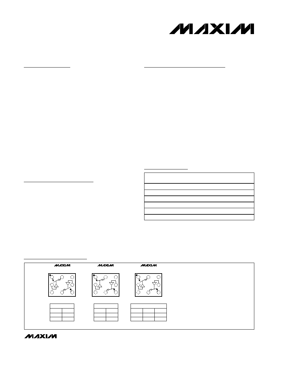
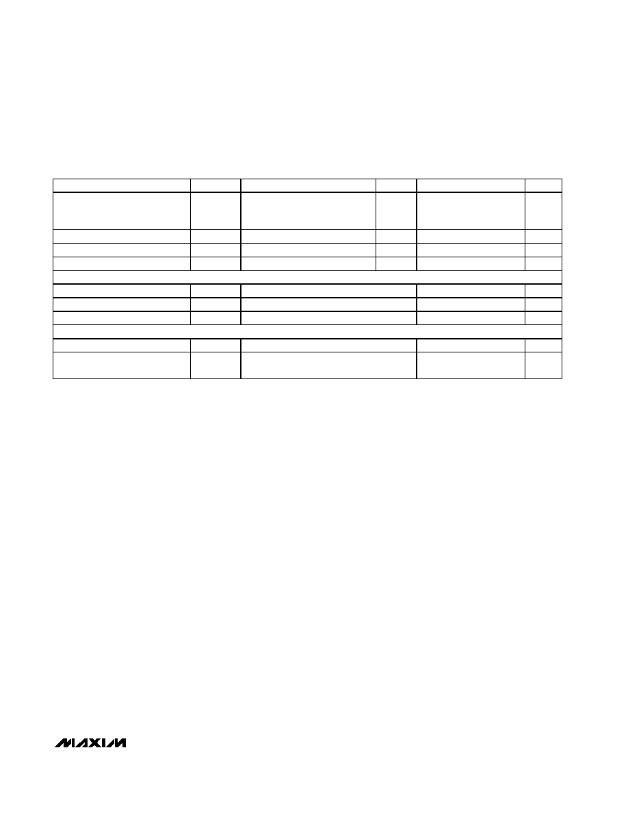
Ordering Information
19-2645; Rev 0; 10/02
For pricing, delivery, and ordering information, please contact Maxim/Dallas Direct! at
1-888-629-4642, or visit Maxim's website at www.maxim-ic.com.
PART
TEMP
RANGE
PIN/BUMP-
PACKAGE
TOP
MARK
MAX4731EUA
-40°C to +85°C
8 µMAX
--
MAX4731EBL-T*
-40°C to +85°C
9 UCSP-9**
ABV
MAX4732EUA
-40°C to +85°C
8 µMAX
--
MAX4732EBL-T*
-40°C to +85°C
9 UCSP-9**
ABT
MAX4733EUA
-40°C to +85°C
8 µMAX
--
MAX4733EBL-T*
-40°C to +85°C
9 UCSP-9**
ABS
NO2
V+
GND
IN2
IN1
NO1
COM1
COM2
TOP VIEW
(BUMPS
ON BOTTOM)
UCSP
MAX4731
A1
B1
C1
C2
C3
B3
A3
A2
MAX4732
MAX4733
NC2
V+
GND
IN2
IN1
NC1
COM1
COM2
UCSP
A1
B1
C1
C2
C3
B3
A3
A2
NC2
V+
GND
IN2
IN1
NO1
COM1
COM2
UCSP
A1
B1
C1
C2
C3
B3
A3
A2
IN_
0
1
NO_
MAX4731
OFF
ON
SWITCHES SHOWN
FOR LOGIC "0" INPUT
IN_
0
1
NC_
MAX4732
ON
OFF
SWITCHES SHOWN
FOR LOGIC "0" INPUT
IN_
0
1
NO1
MAX4733
ON
OFF
SWITCHES SHOWN FOR LOGIC "0" INPUT
NC2
OFF
ON
Pin Configurations/Functional Diagrams/Truth Tables
Note: Requires special solder temperature profile described in
the Absolute Maximum Ratings section.
**UCSP reliability is integrally linked to the user's assembly
methods, circuit board material, and environment. See the UCSP
Reliability section of this data sheet for more information.
UCSP is a trademark of Maxim Integrated Products, Inc.
Rail-to-Rail is a registered trademark of Nippon Motorola, Ltd.
Pin Configurations/Functional Diagrams/
Truth Tables continued at end of data sheet.
*Future product--contact factory for availability.
MAX4731/MAX4732/MAX4733
50
Dual SPST Analog Switches in UCSP
2
_______________________________________________________________________________________
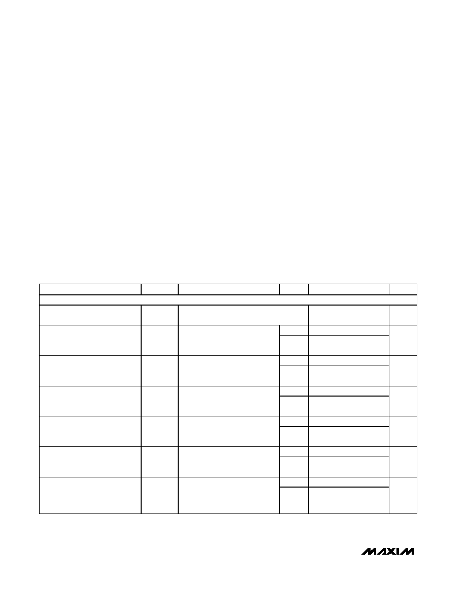
ABSOLUTE MAXIMUM RATINGS
ELECTRICAL CHARACTERISTICS--Single +3V Supply
(V+ = +3V ±10%, V
IH
= +2.0V, V
IL
= +0.8V, T
A
= T
MIN
to T
MAX
, unless otherwise noted. Typical values are at V+ = +3V, T
A
= +25°C.)
(Notes 3, 4)
Stresses beyond those listed under "Absolute Maximum Ratings" may cause permanent damage to the device. These are stress ratings only, and functional
operation of the device at these or any other conditions beyond those indicated in the operational sections of the specifications is not implied. Exposure to
absolute maximum rating conditions for extended periods may affect device reliability.
(All Voltages Referenced to GND)
V+ ...........................................................................-0.3V to +12V
IN_, COM_, NO_, NC_ (Note 1)....................-0.3V to (V+ + 0.3V)
Continuous Current (any pin) ...........................................±10mA
Peak Current (any pin, pulsed at 1ms, 10% duty cycle) ...±20mA
Continuous Power Dissipation (T
A
= +70°C)
8-Pin µMAX (derate 4.5mW/°C above +70°C) .............362mW
9-Bump UCSP (derate 4.7mW/°C above +70°C).........379mW
Operating Temperature Range ...........................-40°C to +85°C
Storage Temperature Range .............................-65°C to +150°C
Maximum Junction Temperature .....................................+150°C
Lead Temperature (soldering, 10s) .................................+300°C
Bump Temperature (soldering, Note 2)
Infrared (15s) ...............................................................+220°C
Vapor Phase (60s) .......................................................+215°C
Note 1: Signals on IN_, NO_, NC_, or COM_ exceeding V+ or GND are clamped by internal diodes. Limit forward-diode current to
maximum current rating.
Note 2: This device is constructed using a unique set of packaging techniques that impose a limit on the thermal profile the device
can be exposed to during board level solder attach and rework. This limit permits only the use of the solder profiles recom-
mended in the industry-standard specification, JEDEC 020A, paragraph 7.6, Table 3 for IR/VPR and Convection reflow. Pre-
heating is required. Hand or wave soldering is not allowed.
PARAMETER
SYMBOL
CONDITIONS
T
A
MIN
TYP
MAX
UNITS
ANALOG SWITCH
Analog Signal Range
V
COM_
,
V
NO_
, V
NC_
0
V+
V
+25°C
19
50
On-Resistance
R
ON
V+ = +2.7V,
I
COM_
= 5mA;
V
NO_
or V
NC_
= +1.5V
T
MIN
to
T
MAX
60
+25°C
0.8
3.5
On-Resistance Matching
Between Channels (Notes 5, 6)
R
ON
V+ = +2.7V,
I
COM_
= 5mA;
V
NO_
or V
NC_
= +1.5V
T
MIN
to
T
MAX
4.5
+25°C
2.3
9
On-Resistance Flatness
(Note 7)
R
FLAT(ON)
V+ = +2.7V,
I
COM_
= 5mA;
V
NO_
or V
NC_
= +1V, +1.5V, +2V
T
MIN
to
T
MAX
11
+25°C
-0.1
+0.1
NO_ or NC_ Off-Leakage Current
(Note 8)
I
NO_(OFF)
I
NC_(OFF)
V+ = +3.6V,
V
COM_
= +0.3V, +3V;
V
NO_
or V
NC_
= +3V, +0.3V
T
MIN
to
T
MAX
-2
+2
nA
+25°C
-0.1
+0.1
COM_ Off-Leakage Current
(Note 8)
I
COM_(OFF)
V+ = +3.6V,
V
COM_
= +0.3V, +3V;
V
NO_
or V
NC_
= +3V, +0.3V
T
MIN
to
T
MAX
-2
+2
nA
+25°C
-0.2
+0.2
COM_ On-Leakage Current
(Note 8)
I
COM_(ON)
V+ = +3.6V,
V
COM_
= +0.3V, +3.0V;
V
NO_
or V
NC_
= +0.3V, +3V, or
floating
T
MIN
to
T
MAX
-4
+4
nA
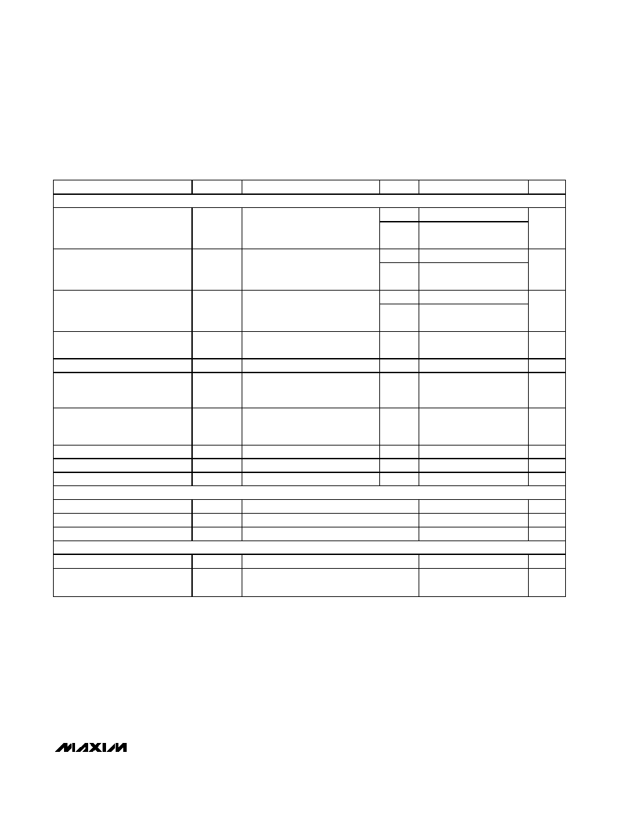
MAX4731/MAX4732/MAX4733
50
Dual SPST Analog Switches in UCSP
_______________________________________________________________________________________
3
ELECTRICAL CHARACTERISTICS--Single +3V Supply (continued)
(V+ = +3V ±10%, V
IH
= +2.0V, V
IL
= +0.8V, T
A
= T
MIN
to T
MAX
, unless otherwise noted. Typical values are at V+ = +3V, T
A
= +25°C.)
(Notes 3, 4)
PARAMETER
SYMBOL
CONDITIONS
T
A
MIN
TYP
MAX
UNITS
DYNAMIC CHARACTERISTICS
+25°C
70
150
Turn-On Time
t
ON
V
NO_
or V
NC_
= +1.5V,
R
L
= 300
,
C
L
= 35pF, Figure 2
T
MIN
to
T
MAX
170
ns
+25°C
30
60
Turn-Off Time
t
OFF
V
NO_
or V
NC_
= +1.5V,
R
L
= 300
, C
L
= 35pF,
Figure 2
T
MIN
to
T
MAX
70
ns
+25°C
40
Break-Before-Make
(MAX4733 Only, Note 8)
t
BBM
V
NO_
or V
NC_
= +1.5V,
R
L
= 300
, C
L
= 35pF,
Figure 3
T
MIN
to
T
MAX
1
ns
Charge Injection
Q
V
GEN
= 0V, R
GEN
= 0, C
L
= 1.0nF,
Figure 4
+25°C
7.5
pC
On-Channel -3dB Bandwidth
BW
Signal = 0dBm, 50
in and out
+25°C
300
MHz
Off-Isolation (Note 9)
V
ISO
f = 1MHz, V
COM_
= 1V
RMS
,
R
L
= 50
, C
L
= 5pF,
Figure 5
+25°C
-72
dB
Crosstalk (Note 10)
V
CT
f = 1MHz, V
COM_
= 1V
RMS
,
R
L
= 50
, C
L
= 5pF,
Figure 6
+25°C
-108
dB
NO_ or NC_ Off-Capacitance
C
OFF
f = 1MHz, Figure 7
+25°C
20
pF
COM_ Off-Capacitance
C
COM_(OFF)
f = 1MHz, Figure 7
+25°C
20
pF
COM_ On-Capacitance
C
COM_(ON)
f = 1MHz, Figure 7
+25°C
40
pF
LOGIC INPUT
Input Logic High
V
IH
2.0
V
Input Logic Low
V
IL
0.8
V
Input Leakage Current
I
IN
V
IN_
= 0V or V+
-1
+0.005
+1
µA
SUPPLY
Power-Supply Range
V+
2.0
11
V
Positive Supply Current
I+
V+ = +5.5V, V
IN_
= 0V or V+,
all switches on or off
0.0001
1
µA
MAX4731/MAX4732/MAX4733
50
Dual SPST Analog Switches in UCSP
4
_______________________________________________________________________________________
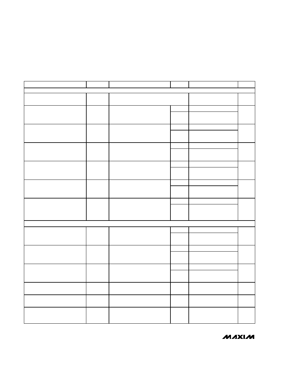
ELECTRICAL CHARACTERISTICS--Single +5V Supply
(V+ = +5V ±10%, V
IH
= +2.0V, V
IL
= +0.8V, T
A
= T
MIN
to T
MAX
, unless otherwise noted. Typical values are at V+ = +5V, T
A
= +25°C.)
(Notes 3, 4)
PARAMETER
SYMBOL
CONDITIONS
T
A
MIN
TYP
MAX
UNITS
ANALOG SWITCH
Analog Signal Range
V
COM_
,
V
NO_
, V
NC_
0
V+
V
+25°C
8.5
25
On-Resistance
R
ON
V+ = +4.5V,
I
COM_
= 5mA,
V
NO_
or V
NC_
= +3.5V
T
MIN
to
T
MAX
30
+25°C
0.2
3
On-Resistance Matching
Between Channels (Notes 5, 6)
R
ON
V+ = +4.5V,
I
COM_
= 5mA,
V
NO_
or V
NC_
= +3.5V
T
MIN
to
T
MAX
4
+25°C
2
5
On-Resistance Flatness
(Note 7)
R
FLAT(ON)
V+ = +4.5V,
I
COM_
= 5mA,
V
NO_
or V
NC_
= +1V, +2V, +3V
T
MIN
to
T
MAX
7
+25°C
-0.1
+0.1
NO_ or NC_ Off-Leakage Current
(Note 8)
I
NO_(OFF)
I
NC_(OFF)
V+ = +5.5V,
V
COM_
= +1V, +4.5V;
V
NO_
or V
NC_
= +4.5V, +1V
T
MIN
to
T
MAX
-2
+2
nA
+25°C
-0.1
+0.1
COM_ Off-Leakage Current
(Note 8)
I
COM_(OFF)
V+ = +5.5V,
V
COM_
= +1V, +4.5V;
V
NO_
or V
NC_
= +4.5V, +1V
T
MIN
to
T
MAX
-2
+2
nA
+25°C
-0.2
+0.2
COM_ On-Leakage Current
(Note 8)
I
COM_(ON)
V+ = +5.5V,
V
COM_
= +1V, +4.5V;
V
NO_
or V
NC_
= +1V, +4.5V, or
floating
T
MIN
to
T
MAX
-4
+4
nA
DYNAMIC CHARACTERISTICS
+25°C
47
85
Turn-On Time
t
ON
V
NO_
or V
NC_
= +3.0V,
R
L
= 300
, C
L
= 35pF,
Figure 2
T
MIN
to
T
MAX
95
ns
+25°C
23
45
Turn-Off Time
t
OFF
V
NO_
or V
NC_
= +3.0V,
R
L
= 300
, C
L
= 35pF,
Figure 2
T
MIN
to
T
MAX
55
ns
+25°C
25
Break-Before-Make
(MAX4733 Only, Note 8)
t
BBM
V
NO_
or V
NC_
= +3.0V,
R
L
= 300
, C
L
= 35pF,
Figure 3
T
MIN
to
T
MAX
1
ns
Charge Injection
Q
V
GEN
= 0V, R
GEN
= 0,
C
L
= 1.0nF, Figure 4
+25°C
7.5
pC
On-Channel Bandwidth
BW
Signal = 0dBm,
50
in and out
+25°C
300
MHz
Off-Isolation (Note 9)
V
ISO
f = 1MHz, V
COM_
= 1V
RMS
,
R
L
= 50
, C
L
= 5pF,
Figure 5
+25°C
-72
dB
MAX4731/MAX4732/MAX4733
50
Dual SPST Analog Switches in UCSP
_______________________________________________________________________________________
5
Note 3:
The algebraic convention, where the most negative value is a minimum and the most positive value a maximum, is used
in this data sheet.
Note 4:
UCSP parts are 100% tested at +25°C only, and guaranteed by design over temperature. µMAX parts are 100% tested at
+85°C and +25°C and guaranteed by design over temperature.
Note 5:
R
ON
= R
ON(MAX)
- R
ON(MIN)
.
Note 6:
UCSP on-resistance matching between channels and on-resistance flatness guaranteed by design.
Note 7:
Flatness is defined as the difference between the maximum and minimum value of on-resistance as measured over the
specified analog signal range.
Note 8:
Guaranteed by design.
Note 9:
Off-Isolation = 20 log
10
(V
NO_
/V
COM_
), V
NO_
= output, V
COM_
= input to off switch.
Note 10: Between any two switches.
ELECTRICAL CHARACTERISTICS--Single +5V Supply
(V+ = +5V ±10%, V
IH
= +2.0V, V
IL
= +0.8V, T
A
= T
MIN
to T
MAX
, unless otherwise noted. Typical values are at V+ = +5V, T
A
= +25°C.)
(Notes 3, 4)
PARAMETER
SYMBOL
CONDITIONS
T
A
MIN
TYP
MAX
UNITS
Crosstalk (Note 10)
V
CT
f = 1MHz, V
COM_
= 1V
RMS
,
R
L
= 50
, C
L
= 5pF,
Figure 6
+25°C
-108
dB
NO_ or NC_ Off-Capacitance
C
OFF
f = 1MHz, Figure 7
+25°C
20
pF
COM_ Off-Capacitance
C
COM_(OFF)
f = 1MHz, Figure 7
+25°C
20
pF
COM_ On-Capacitance
C
COM_(ON)
f = 1MHz, Figure 7
+25°C
40
pF
LOGIC INPUT
Input Logic High
V
IH
2.0
V
Input Logic Low
V
IL
0.8
V
Input Leakage Current
I
IN
V
IN_
= 0V or V+
-1
+0.005
+1
µA
SUPPLY
Power-Supply Range
V+
2.0
11
V
Positive Supply Current
I+
V+ = +5.5V, V
IN_
= 0V or V+,
all switches on or off
0.0001
1
µA