 | –≠–ª–µ–∫—Ç—Ä–æ–Ω–Ω—ã–π –∫–æ–º–ø–æ–Ω–µ–Ω—Ç: MAX4781 | –°–∫–∞—á–∞—Ç—å:  PDF PDF  ZIP ZIP |

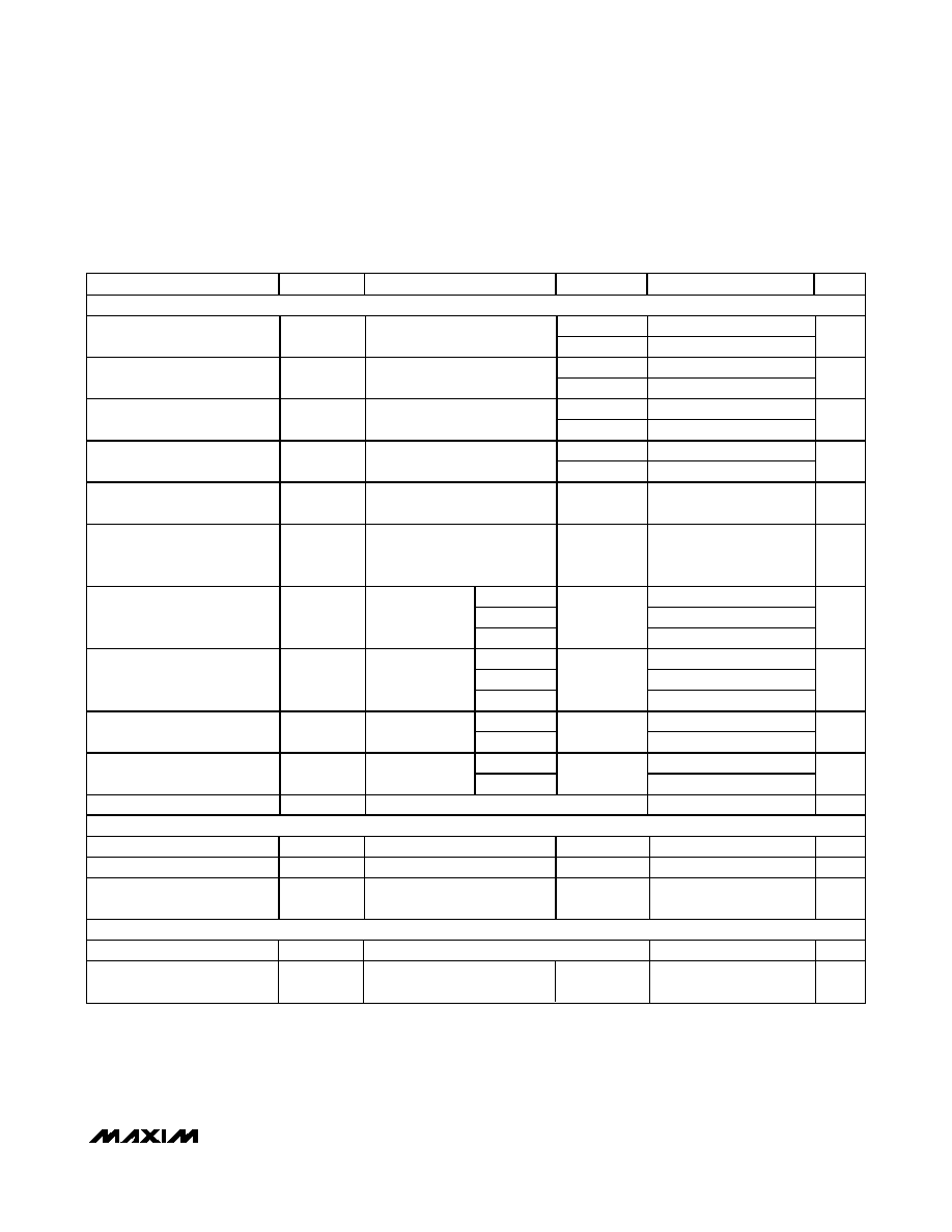
16
15
14
13
4
3
2
1
8
7
6
5
12
11
10
9
X
X7
X5
ENABLE
N.C.
GND
C
B
A
X3
X0
X1
X2
V
CC
X4
X6
3mm x 3mm THIN QFN
LOGIC
16
15
14
13
12
11
10
9
1
2
3
4
5
6
7
8
LOGIC
X4
X6
X
X7
X5
ENABLE
N.C.
GND
V
CC
X2
X1
X0
X3
A
B
C
TSSOP
MAX4781
MAX4781
TOP VIEW
MAX4781/MAX4782/MAX4783
High-Speed, Low-Voltage, 0.7
CMOS Analog
Switches/Multiplexers
________________________________________________________________ Maxim Integrated Products
1
19-2522; Rev 3; 2/05
For pricing delivery, and ordering information please contact Maxim/Dallas Direct! at
1-888-629-4642, or visit Maxim's website at www.maxim-ic.com.
General Description
The MAX4781/MAX4782/MAX4783 are high-speed,
low-voltage, low on-resistance, CMOS analog multiplex-
ers/switches configured as an 8-channel multiplexer
(MAX4781), two 4-channel multiplexers (MAX4782),
and three single-pole/double-throw (SPDT) switches
(MAX4783).
These devices operate with a +1.6V to +3.6V single
supply. When powered from a +3V supply, MAX4781/
MAX4782/MAX4783 feature a 0.7
on-resistance
(R
ON
), with 0.3
R
ON
matching between channels, and
0.1
R
ON
flatness. These devices handle rail-to-rail
analog signals while consuming less than 3µW of qui-
escent power. They are available in space-saving 16-
pin thin QFN (3mm x 3mm) and TSSOP packages.
Applications
Battery-Operated Equipment
Audio Signal Routing
Low-Voltage Data-Acquisition Systems
Communications Circuits
Features
On-Resistance
0.7
(+3V Supply)
1.6
(+1.8V Supply)
On-Resistance Match Between Channels
0.3
(+3V Supply)
On-Resistance Flatness
0.1
(+3V Supply)
Single-Supply Operation Down to 1.6V
High-Current Handling Capacity (150mA
Continuous)
+1.8V CMOS-Logic Compatible
Fast Switching Times: t
ON
= 11ns, t
OFF
= 4ns
Pin Compatible with Industry-Standard
74HC4051/74HC4052/74HC4053 and
MAX4617/MAX4618/MAX4619
Available in 3mm x 3mm 16-Pin Thin QFN Packages
Ordering Information
Pin Configurations/Functional Diagrams continued at end of data sheet.
PART
TEMP RANGE
PIN-PACKAGE
MAX4781EUE
-40
∞C to +85∞C 16 TSSOP
MAX4781ETE
-40
∞C to +85∞C 16 Thi n QFN ( 3m m x 3m m )
MAX4782EUE
-40
∞C to +85∞C 16 TSSOP
MAX4782ETE
-40
∞C to +85∞C 16 Thi n QFN ( 3m m x 3m m )
MAX4783EUE
-40
∞C to +85∞C 16 TSSOP
MAX4783ETE
-40
∞C to +85∞C 16 Thi n QFN ( 3m m x 3m m )
Pin Configurations/Functional Diagrams

MAX4781/MAX4782/MAX4783
High-Speed, Low-Voltage, 0.7
CMOS Analog
Switches/Multiplexers
2
_______________________________________________________________________________________
ABSOLUTE MAXIMUM RATINGS
ELECTRICAL CHARACTERISTICS--Single +3V Supply
(V
CC
= +2.7V to +3.6V, GND = 0, V
IH
= 1.4V, V
IL
= 0.5V, T
A
= T
MIN
to T
MAX
, unless otherwise noted. Typical values are at
T
A
= +25∞C.) (Notes 2, 3)
Stresses beyond those listed under "Absolute Maximum Ratings" may cause permanent damage to the device. These are stress ratings only, and functional
operation of the device at these or any other conditions beyond those indicated in the operational sections of the specifications is not implied. Exposure to
absolute maximum rating conditions for extended periods may affect device reliability.
Voltages Referenced to GND
V
CC
, A, B, C, and ENABLE ...............................-0.3V to +4.6V
Voltage at Any Other Terminal
(Note 1)...................................................-0.3V to (V
CC
+ 0.3V)
Continuous Current into A, B, C, ENABLE........................±10mA
Continuous Current into X, Y, Z, X_, Y_, Z_ ....................±150mA
Peak Current into X, Y, Z, X_, Y_, Z_
(pulsed at 1ms, 10% duty cycle)................................±300mA
Continuous Power Dissipation
16-Pin Thin QFN (derate 16.9mW/∞C above +70∞C) ...1349mW
16-Pin TSSOP (derate 5.7mW/∞C above +70∞C) ........ 457mW
Operating Temperature Range ..........................-40∞C to +85∞C
Junction Temperature ......................................................+150∞C
Storage Temperature Range .............................-65∞C to +150∞C
Lead Temperature (soldering, 10s) .................................+300∞C
Note 1: Signals on X, Y, Z, X_, Y_, and Z_ exceeding V
CC
or GND are clamped by internal diodes. Limit forward-diode current to
maximum current rating.
PARAMETER
SYMBOL
CONDITIONS
T
A
MIN
TYP
MAX
UNITS
ANALOG SWITCH
Analog Signal Range
V
X
, V
Y
, V
Z
,
V
X
_, V
Y
_, V
Z
_
0
V
CC
V
+25∞C
0.7
1
On-Resistance (Note 4)
R
ON
V
C C
= + 2.7V ; I
X _
, I
Y _
, I
Z _
=
100m A; V
X
, V
Y
, V
Z
=
1.7V
T
MIN
to T
MAX
1.2
+25∞C
0.3
0.4
On-Resistance Match
Between Channels
(Notes 4, 5)
R
ON
V
C C
= + 2.7V ; I
X _
, I
Y _
, I
Z _
=
100m A; V
X
, V
Y
, V
Z
=
1.7V
T
MIN
to T
MAX
0.6
+25∞C
0.1
0.2
On-Resistance Flatness
(Note 6)
R
FLAT(ON)
V
C C
= + 2.7V ; I
X _
, I
Y _
, I
Z _
=
100m A; V
X
, V
Y
, V
Z
= 0, 0.7V,
1.7V
T
MIN
to T
MAX
0.2
+25∞C
-2
0.002
+2
X_, Y_, Z_
Off-Leakage Current
I
X_(OFF)
I
Y_(OFF)
I
Z_(OFF)
V
C C
= + 3.6V ;
V
X _
, V
Y_
, V
Z_
= 3.3V , 0.3V ; V
X
,
V
Y
, V
Z
= 0.3V, 3.3V
T
MIN
to T
MAX
-7
+7
nA
+25∞C
-2
0.002
+2
X Off-Leakage Current
(MAX4781 Only)
I
X(OFF)
V
C C
= + 3.6V ;
V
X_
= 3.3V , 0.3V ;
V
X_
= 0.3V, 3.3V
T
MIN
to T
MAX
-50
+50
nA
+25∞C
-2
0.002
+2
X On-Leakage Current
(MAX4781 Only)
I
X(ON)
V
C C
= +3.6V
V
X_
= 0.3V , 3.3V ;
V
X_
= 0.3V , 3.3V or fl oati ng
T
MIN
to T
MAX
-50
+50
nA
+25∞C
-2
0.002
+2
X, Y, Z Off-Leakage Current
(MAX4782/MAX4783 Only)
I
X(OFF)
I
Y(OFF)
I
Z(OFF)
V
C C
= + 3.6V ;
V
X _
, V
Y_
, V
Z_
= 3.3V , 0.3V ; V
X
,
V
Y
, V
Z
= 0.3V, 3.3V
T
MIN
to T
MAX
-25
+25
nA
+25∞C
-2
0.002
+2
X, Y, Z On-Leakage Current
(MAX4782/MAX4783 Only)
I
X(ON)
I
Y(ON)
I
Z(ON)
V
C C
= + 3.6V ;
V
X
, V
Y
, V
Z
= 0.3V , 3.3V ; V
X
, V
Y
,
V
Z
= 0.3V, 3.3V or floating
T
MIN
to T
MAX
-25
+25
nA
MAX4781/MAX4782/MAX4783
High-Speed, Low-Voltage, 0.7
CMOS Analog
Switches/Multiplexers
_______________________________________________________________________________________
3
ELECTRICAL CHARACTERISTICS--Single +3V Supply (continued)
(V
CC
= +2.7V to +3.6V, GND = 0, V
IH
= 1.4V, V
IL
= 0.5V, T
A
= T
MIN
to T
MAX
, unless otherwise noted. Typical values are at T
A
=
+25∞C.) (Notes 2, 3)
PARAMETER
SYMBOL
CONDITIONS
T
A
MIN
TYP
MAX
UNITS
SWITCH DYNAMIC CHARACTERISTICS
+25∞C
11
25
Turn-On Time
t
ON
V
X _
, V
Y _
, V
Z _
= 1.5V ; R
L
= 50
;
C
L
= 35pF; Figure 1
T
MIN
to T
MAX
27
ns
+25∞C
4
15
Turn-Off Time
t
OFF
V
X _
, V
Y _
, V
Z _
= 1.5V ; R
L
= 50
;
C
L
= 35pF; Figure 1
T
MIN
to T
MAX
20
ns
+25∞C
11
25
Address Transition Time
t
TRANS
V
X _
, V
Y _
, V
Z _
= 1.5V ; R
L
= 50
;
C
L
= 35pF; Figure 2
T
MIN
to T
MAX
27
ns
+25∞C
18
Break-Before-Make Time
(Note 7)
t
BBM
V
X _
, V
Y _
, V
Z _
= 1.5V ; R
L
= 50
;
C
L
= 35pF; Figure 3
T
MIN
to T
MAX
2
ns
Charge Injection
Q
V
GE N
= 0, R
GE N
= 0, C
L
= 1nF,
Figure 4
+25∞C
-110
pC
Input Off-Capacitance
C
X_(OFF),
C
Y_(OFF),
C
Z_(OFF)
f = 1MHz,
Figure 6
+25∞C
38
pF
MAX4781
310
MAX4782
158
Output Off-Capacitance
C
X(OFF),
C
Y(OFF),
C
Z(OFF)
f = 1MHz,
Figure 6
MAX4783
+25∞C
75
pF
MAX4781
380
MAX4782
224
Output On-Capacitance
C
X(ON)
C
Y(ON)
C
Z(ON)
f = 1MHz,
Figure 6
MAX4783
+25∞C
140
pF
f = 10MHz
-75
Off-Isolation (Note 8)
V
ISO
R
L
= 50
, C
L
=
35pF, Figure 5
f = 1MHz
-90
dB
f = 10MHz
-65
Channel-to-Channel Crosstalk
(Note 9)
V
CT
R
L
= 50
, C
L
=
35pF, Figure 5
f = 1MHz
-80
dB
Total Harmonic Distortion
THD
f = 20Hz to 20kHz, 0.5V
P-P
, R
L
= 32
0.045
%
DIGITAL I/O
Input Logic High
V
IH
T
MIN
to T
MAX
1.4
V
Input Logic Low
V
IL
T
MIN
to T
MAX
0.5
V
Input Leakage Current
I
IN
_
V
A
, V
B
, V
C
= V
E N A B L E
= 0 or
3.6V
T
MIN
to T
MAX
-1
0.0005
+1
µA
POWER SUPPLY
Power-Supply Range
V
CC
+1.6
+3.6
V
Positive Supply Current
I
CC
V
CC
= 3.6V; V
A
, V
B
, V
C
;
V
E N A B L E
= 3.6V or 0
1
µA
MAX4781/MAX4782/MAX4783
High-Speed, Low-Voltage, 0.7
CMOS Analog
Switches/Multiplexers
4
_______________________________________________________________________________________
ELECTRICAL CHARACTERISTICS--Single +1.8V Supply
(V
CC
= +1.8V, GND = 0, V
IH
= 1V, V
IL
= 0.4V, T
A
= T
MIN
to T
MAX
, unless otherwise noted. Typical values are at T
A
= +25∞C.) (Notes 2, 3)
PARAMETER
SYMBOL
CONDITIONS
T
A
MIN
TYP
MAX
UNITS
ANALOG SWITCH
Analog Signal Range
V
X
_, V
Y
_
,
V
Z
_, V
X
,
V
Y
, V
Z
0
V
CC
V
+25∞C
1.6
2.5
On-Resistance (Note 4)
R
ON
V
CC
= 1.8V; I
X_
, I
Y_
, I
Z_
= 10mA;
V
X
, V
Y
, V
Z
= 1.0V
T
M IN
to T
M AX
3.5
+25∞C
0.3
0.4
On-Resistance Match Between
Channels (Notes 4, 5)
R
ON
V
CC
= 1.8V; I
X_
, I
Y_
, I
Z_
= 10mA;
V
X
, V
Y
, V
Z
= 1.0V
T
M IN
to T
M AX
0.6
SWITCH DYNAMIC CHARACTERISTICS
+25∞C
17
30
Turn-On Time
t
ON
V
X_
, V
Y_
, V
Z_
= 1.0V; R
L
= 50
;
C
L
= 35pF; Figure 1
T
M IN
to T
M AX
32
ns
+25∞C
8
20
Turn-Off Time
t
OFF
V
X_
, V
Y_
, V
Z_
= 1.0V; R
L
= 50
;
C
L
= 35pF; Figure 1
T
M IN
to T
M AX
22
ns
+25∞C
17
30
Address Transition Time
t
TRANS
V
X_
, V
Y_
, V
Z_
= 1.0V; R
L
= 50
;
C
L
= 35pF; Figure 2
T
M IN
to T
M AX
32
ns
+25∞C
26
Break-Before-Make Time
(Note 7)
t
BBM
V
X_
, V
Y_
, V
Z_
= 1V; R
L
= 50
;
C
L
= 35pF; Figure 3
T
M IN
to T
M AX
1
ns
Charge Injection
Q
V
GEN
= 0, R
GEN
= 0, C
L
= 1nF,
Figure 4
+25∞C
-40
pC
DIGITAL I/O
Input Logic High
V
IH
T
M IN
to T
M AX
1
V
Input Logic Low
V
IL
T
M IN
to T
M AX
0.4
V
Input Leakage Current
I
IN
_
V
A
, V
B
, V
C
= V
E N A B L E
= 0 or 3.6V T
M IN
to T
M AX
-1
0.000
+1
µA
POWER SUPPLY
Power-Supply Range
V
CC
1.6
3.6
V
Positive Supply Current
I
CC
V
CC
= 3.6V; V
A
, V
B
, V
C
,
V
E N A B L E
= 0 or 3.6V
1
µA
Note 2: The algebraic convention is used in this data sheet; the most negative value is shown in the minimum column.
Note 3: Devices are tested at maximum hot temperature and are guaranteed by design and correlation at T
A
= +25∞C and -40∞C
specifications.
Note 4: R
ON
and
R
ON
matching specifications for thin QFN-packaged parts are guaranteed by design.
Note 5:
R
ON
= R
ON(MAX)
- R
ON(MIN).
Note 6: Flatness is defined as the difference between the maximum and minimum value of on-resistance as measured over the
specified analog signal ranges.
Note 7: Guaranteed by design; not production tested.
Note 8: Off-isolation = 20log10(V
COM_
/ V
NO
), V
COM_
= output, V
NO
= input to off switch.
Note 9: Between any two channels.

MAX4781/MAX4782/MAX4783
High-Speed, Low-Voltage, 0.7
CMOS Analog
Switches/Multiplexers
_______________________________________________________________________________________
5
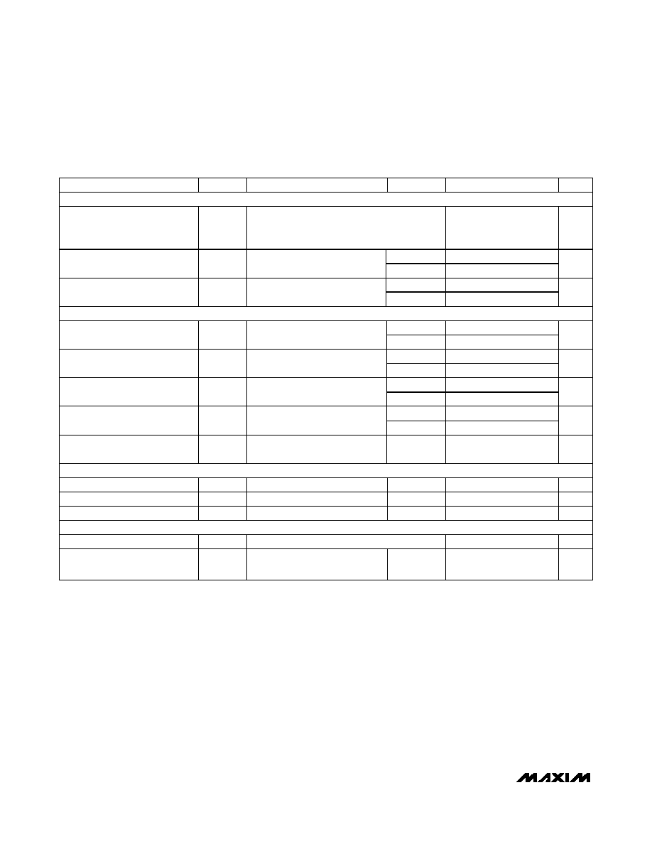
ON-RESISTANCE vs. V
X
, V
Y
, V
Z
MAX4781 toc01
V
X
, V
Y
, V
Z
(V)
R
ON
(
)
3.2
2.8
0.4 0.8 1.2
2.0
1.6
2.4
0.6
0.8
1.0
1.2
1.4
1.6
1.8
2.0
0.4
0
3.6
V
CC
= 1.8V
V
CC
= 2.0V
V
CC
= 2.5V
V
CC
= 2.7V
V
CC
= 3.6V
V
CC
= 3.3V
V
CC
= 3.0V
ON-RESISTANCE vs. V
X
, V
Y
, V
Z
,
AND TEMPERATURE
MAX4781 toc02
V
X
, V
Y
, V
Z
(V)
R
ON
(
)
2.5
0.5
1.0
1.5
2.0
0.1
0.2
0.3
0.4
0.6
0.5
0.7
0.9
0.8
1.0
0
0
3.0
T
A
= +85
∞C
T
A
= +25
∞C
T
A
= -40
∞C
V
CC
= 3.0V
1
-40
85
60
10
35
-15
LEAKAGE CURRENT vs. TEMPERATURE
100
1000
10
MAX4781toc03
TEMPERATURE (
∞C)
I
X
, I
Y
, I
Z
(pA)
ON
OFF
V
CC
= 3.6V
CHARGE INJECTION vs. V
X
, V
Y
, V
Z
MAX4781 toc04
V
X
, V
Y
, V
Z
(V)
CHARGE INJECTION (pC)
2.5
0.5
1.0
1.5
2.0
-100
-80
-60
-20
-40
0
40
20
60
-120
0
3.0
V
CC
= 1.8V
V
CC
= 3.0V
1000
1.6
2.0
2.4
2.8
3.2
3.6
100
10
1
0.1
0.01
SUPPLY CURRENT vs. TEMPERATURE
MAX4781 toc05
V
CC
(V)
I
CC
(nA)
T
A
= -40
∞C
T
A
= +25
∞C
T
A
= +85
∞C
LOGIC THRESHOLD
vs. SUPPLY VOLTAGE
MAX4781 toc06
SUPPLY VOLTAGE (V)
LOGIC THRESHOLD (V)
2.1
2.6
3.1
0.6
0.7
0.9
0.8
1.0
1.1
1.2
0.5
1.6
3.6
RISING
FALLING
TURN-ON/TURN-OFF TIME
vs. SUPPLY VOLTAGE
MAX4781 toc07
SUPPLY VOLTAGE (V)
TIME (ns)
2.0
2.4
2.8
3.2
5
15
10
20
25
0
1.6
3.6
t
ON
t
OFF
TURN-ON/TURN-OFF TIME
vs. TEMPERATURE
MAX4781 toc08
TEMPERATURE (
∞C)
TIME (ns)
-15
10
35
60
2
8
6
4
10
12
14
0
-40
85
t
ON
t
OFF
V
CC
= 3.0V
Typical Operating Characteristics
(GND = 0, T
A
= +25∞C, unless otherwise noted.)