Äîêóìåíòàöèÿ è îïèñàíèÿ www.docs.chipfind.ru
General Description
The MAX4789MAX4794 family of switches feature
internal current limiting to prevent damage to host
devices due to faulty load conditions. These analog
switches have a low 0.2
on-resistance and operate
from 2.3V to 5.5V input voltage range. They are avail-
able with guaranteed 200mA, 250mA, and 300mA cur-
rent limits, making them ideal for SDIO and other load
switching applications.
When the switch is on and a load is connected to the
port, a guaranteed blanking time of 14ms ensures that
the transient voltages settle down. If after this blanking
time the load current is greater than the current limit,
the MAX4789, MAX4791, and MAX4793 enter a latch-
off state where the switch is turned off and FLAG is
issued to the microprocessor. The switch can be turned
on again by cycling the power or the ON pin.
The MAX4790, MAX4792, and MAX4794 have an
autoretry feature where the switch turns off after the
blanking time and then continuously checks to see if
the overload condition is present. The switch remains
on after the overload condition disappears.
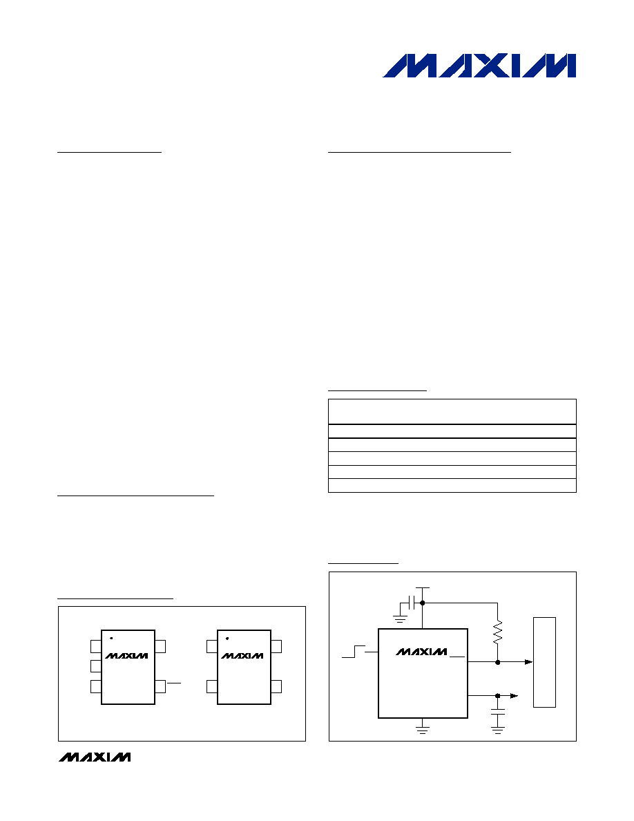
The MAX4789MAX4794 are available in 6-pin 3mm x
3mm TDFN and tiny space-saving 4-pin SOT143 pack-
ages. The MAX4789/MAX4791/MAX4793 are also avail-
able in a tiny 5-pin SOT23 package. For lower current
current-limiting switches, refer to the MAX4785MAX4788
data sheet.
Applications
PDAs and Palmtop Devices
Cell Phones
GPS Systems
Hand-Held Devices
SDIO
Features
Guaranteed Current Limit: 200mA, 250mA, 300mA
Thermal-Shutdown Protection
Reverse Current Protection
0.2 On-Resistance
14ms Guaranteed Blanking Time
FLAG Function (MAX4789/MAX4791/MAX4793)
80µA Supply Current
8µA Latch-Off Current
(MAX4789/MAX4791/MAX4793)
0.01µA Shutdown Current
2.3V to 5.5V Supply Range
Undervoltage Lockout
Fast Current-Limit Response Time (5µs)
TDFN and SOT23/SOT143 Packages
MAX4789MAX4794
200mA/250mA/300mA Current-Limit Switches
________________________________________________________________ Maxim Integrated Products
1
Ordering Information
2.3V TO 5.5V
IN
OUT
FLAG
GND
ON
µP
TO SDIO PORT
MAX4789
MAX4791
MAX4793
Typical Operating Circuit
19-2663; Rev 2; 2/05
For pricing, delivery, and ordering information, please contact Maxim/Dallas Direct! at
1-888-629-4642, or visit Maxim's website at www.maxim-ic.com.
*EP = Exposed pad.
Ordering Information continued at end of data sheet.
Selector Guide appears at end of data sheet.
PART
TEMP RANGE
PIN-PACKAGE
TOP
MARK
MAX4789EUS-T
-40°C to +85°C
4 SOT143-4
KAFE
MAX4789EUK-T
-40°C to +85°C
5 SOT23-5
AEAC
MAX4789ETT
-40°C to +85°C
6 TDFN-EP*
ABO
MAX4790EUS-T
-40°C to +85°C
4 SOT143-4
KAFF
MAX4790ETT
-40°C to +85°C
6 TDFN-EP
ABP
GND
FLAG
Pin Configurations continued at end of data sheet.
1
5 OUT
IN
MAX4789
MAX4791
MAX4793
SOT23
TOP VIEW
2
3
4
ON
ON
1
4 IN
OUT
MAX4789
MAX4794
SOT143
2
3
GND
Pin Configurations
MAX4789MAX4794
200mA/250mA/300mA Current-Limit Switches
2
_______________________________________________________________________________________
ABSOLUTE MAXIMUM RATINGS
ELECTRICAL CHARACTERISTICS
(V
IN
= 2.3V to 5.5V, T
A
= -40°C to +85°C, unless otherwise noted. Typical values are at V
IN
= 3.3V, T
A
= +25°C.) (Note 1)
Stresses beyond those listed under "Absolute Maximum Ratings" may cause permanent damage to the device. These are stress ratings only, and functional
operation of the device at these or any other conditions beyond those indicated in the operational sections of the specifications is not implied. Exposure to
absolute maximum rating conditions for extended periods may affect device reliability.
IN, ON, FLAG, OUT to GND .....................................-0.3V to +6V
OUT Short Circuit to GND .................................Internally Limited
Continuous Power Dissipation (T
A
= +70°C)
4-Pin SOT143 (derate 4.0mW/°C above +70°C)..........320mW
5-Pin SOT23 (derate 7.1mW/°C above +70°C)............571mW
6-Pin TDFN (derate 24.4mW/°C above +70°C).........1951.2mW
Operating Temperature Range ...........................-40°C to +85°C
Junction Temperature ......................................................+150°C
Storage Temperature Range .............................-65°C to +150°C
Lead Temperature (soldering, 10s) .................................+300°C
PARAMETER
SYMBOL
CONDITIONS
MIN
TYP
MAX
UNITS
Operating Voltage
V
IN
2.3
5.5
V
V
IN
= +2.3V to +5.0V
80
120
Quiescent Current
I
Q
V
ON
= V
IN
, I
OUT
= 0,
switch on
V
IN
= +5.0V to +5.5V
160
µA
Latch-Off Current (Note 2)
I
LATCH
V
ON
= V
IN
, after an overcurrent fault
(MAX4789/MAX4791/MAX4793)
8
15
µA
Shutdown Current
I
SHDN
V
ON
= 0V
0.01
1
µA
MAX4789/MAX4790
200
300
MAX4791/MAX4792
250
375
Forward Current Limit
MAX4793/MAX4794
300
450
mA
MAX4789/MAX4790
300
MAX4791/MAX4792
375
Reverse Current Limit
MAX4793/MAX4794
450
mA
ON Input Leakage
V
ON
= V
IN
or GND
-1
+1
µA
Off Switch Leakage
V
ON
= 0V, V
OUT
= 0V
0.01
1
µA
Undervoltage Lockout
UVLO
Rising edge
1.8
2.2
V
Undervoltage Lockout Hysteresis
100
mV
T
A
= +25°C, I
OUT
= 100mA
0.2
0.4
On-Resistance
R
ON
T
A
= - 40° C to + 85°C , I
OU T
= 100m A
0.5
ON Input Logic High Voltage
V
IH
2.0
V
ON Input Logic Low Voltage
V
IL
0.8
V
FLAG Output Logic Low Voltage
I
S IN K
= 1m A ( M AX 4789/M AX 4791/M AX 4793) 0.4
V
FLAG Output High Leakage
Current
V
IN
= V
FLAG
= 5.5V
(MAX4789/MAX4791/MAX4793)
1
µA
Thermal Shutdown
150
°C
Thermal-Shutdown Hysteresis
15
°C
DYNAMIC
Turn-On Time (Note 3)
V
ON
from low to high; I
OUT
= 10mA,
C
L
= 0.1µF
100
µs
Turn-Off Time (Note 3)
V
ON
from high to low; I
OUT
= 10mA,
C
L
= 0.1µF
40
ns
MAX4789MAX4794
200mA/250mA/300mA Current-Limit Switches
_______________________________________________________________________________________
3
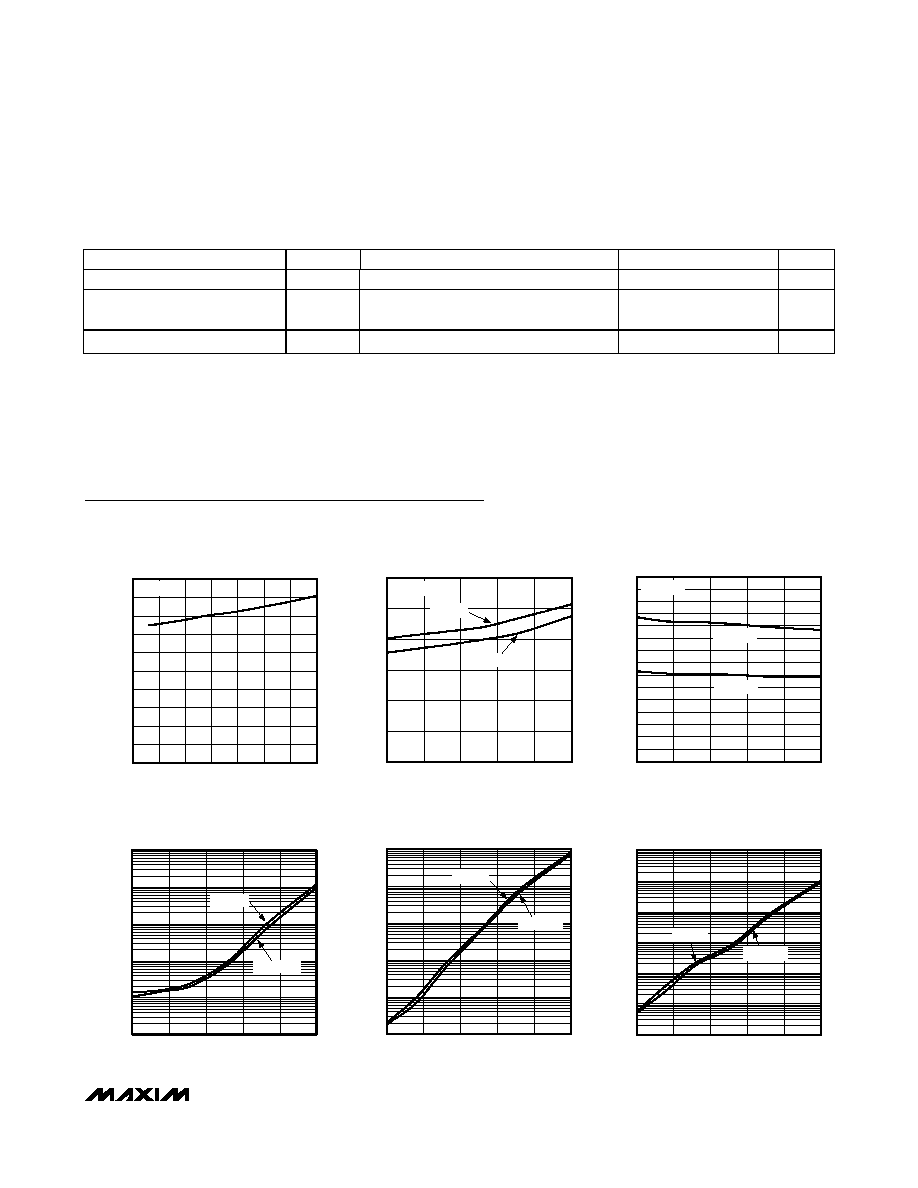
QUIESCENT SUPPLY CURRENT
vs. SUPPLY VOLTAGE
MAX4789 toc01
SUPPLY VOLTAGE (V)
SUPPLY CURRENT (
µ
A)
5.5
5.0
4.0
4.5
3.0
3.5
2.5
10
20
30
40
50
60
70
80
90
100
0
2.0
V
ON
= V
IN
SUPPLY CURRENT
vs. TEMPERATURE
MAX4789 toc02
TEMPERATURE (
°C)
SUPPLY CURRENT (
µ
A)
60
35
10
-15
20
40
60
80
100
120
0
-40
85
V
ON
= V
IN
V
IN
= 5V
V
IN
= 3.3V
LATCH-OFF CURRENT
vs. TEMPERATURE
MAX4789 toc03
TEMPERATURE (
°C)
LATCH-OFF (
µ
A)
60
35
10
-15
1
2
3
4
5
6
7
8
9
10
11
12
13
15
14
0
-40
85
V
ON
= V
IN
V
IN
= 5V
V
IN
= 3.3V
100
10
0.001
-40
85
SHUTDOWN SUPPLY CURRENT
vs. TEMPERATURE
0.01
0.1
1
MAX4789 toc04
TEMPERATURE (
°C)
SHUTDOWN SUPPLY CURRENT (nA)
60
35
10
-15
V
CC
= 5V
V
CC
= 3.3V
10
-40
85
1
0.1
0.01
0.001
0.0001
SHUTDOWN LEAKAGE CURRENT
vs. TEMPERATURE
MAX4789 toc05
TEMPERATURE (
°C)
SHUTDOWN LEAKAGE CURRENT (nA)
60
35
10
-15
V
IN
= 5V
V
IN
= 3.3V
LATCH-OFF LEAKAGE CURRENT
vs. TEMPERATURE
MAX4789 toc06
TEMPERATURE (
°C)
LATCH-OFF LEAKAGE CURRENT (nA)
60
35
10
-15
0.001
0.01
0.1
1
10
100
0.0001
-40
85
V
IN
= 5V
V
IN
= 3.3V
Typical Operating Characteristics
(V
IN
= 3.3V, T
A
= +25°C, unless otherwise noted.)
Note 1: All parts are 100% tested at +25°C. Limits across the full temperature range are guaranteed by design and correlation.
Note 2: Latch-off current does not include the current flowing into FLAG.
Note 3: The on time is defined as the time taken for the current through the switch to go from 0mA to full load. The off-time is defined
as the time taken for the current through the switch to go from full load to 0mA.
Note 4: Retry time is typically 7 times the blanking time.
ELECTRICAL CHARACTERISTICS (continued)
(V
IN
= 2.3V to 5.5V, T
A
= -40°C to +85°C, unless otherwise noted. Typical values are at V
IN
= 3.3V, T
A
= +25°C.) (Note 1)
PARAMETER
SYMBOL
CONDITIONS
MIN
TYP
MAX
UNITS
Blanking Time
t
BLANK
Overcurrent fault (Figures 2, 3)
14
60
ms
Short-Circuit Current-Limit
Response Time
V
ON
= V
IN
= 3.3V, short circuit applied to
OUT
5
µs
Retry Time (Note 4)
t
RETRY
MAX4790/MAX4792/MAX4794 (Figure 2)
98
420
ms
MAX4789MAX4794
200mA/250mA/300mA Current-Limit Switches
4
_______________________________________________________________________________________
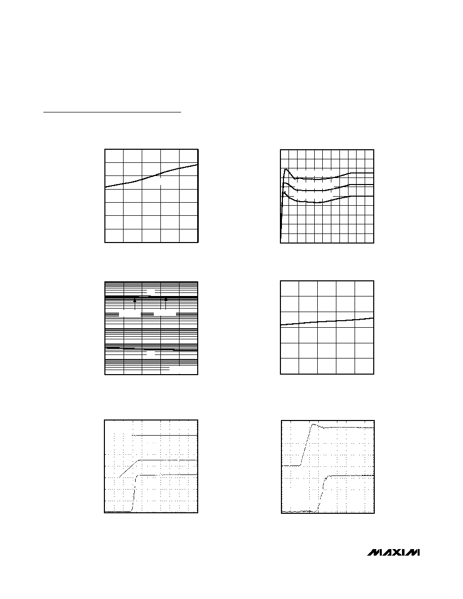
NORMALIZED ON-RESISTANCE
vs. TEMPERATURE
MAX4789 toc07
TEMPERATURE (
°C)
NORMALIZED R
ON
60
35
10
-15
0.2
0.4
0.6
0.8
1.0
1.2
1.4
0
-40
85
V
CC
= 5V
OUTPUT CURRENT
vs. OUTPUT VOLTAGE
MAX4789 toc08
V
IN
- V
OUT
(V)
OUTPUT CURRENT (mA)
3.0
2.7
2.1 2.4
0.6 0.9 1.2 1.5 1.8
0.3
50
100
150
200
250
300
350
400
450
500
0
0
3.3
MAX4793/MAX4794
MAX4789/MAX4790
MAX4791/MAX4792
SWITCH TURN-ON/OFF TIMES
vs. TEMPERATURE
MAX4789 toc09
TEMPERATURE (
°C)
TURN-ON/OFF TIMES (
µ
s)
60
35
10
-15
0.01
0.1
1
10
100
1000
0.001
-40
85
I
LOAD
= 10mA
OFF
ON
V
CC
= 3.3V
V
CC
= 5V
FLAG-BLANKING TIMEOUT
vs. TEMPERATURE
MAX4789 toc10
TEMPERATURE (
°C)
FLAG-BLANKING TIME (ms)
60
35
10
-15
25
30
35
40
45
50
20
-40
85
CURRENT-LIMIT RESPONSE
MAX4789 toc11
40
µs/div
V
IN
2V/div
V
ON
2V/div
I
OUT
100mA/div
V
IN
= 3.3V
C
IN
= 1
µF
C
OUT
= 1
µF
CURRENT-LIMIT RESPONSE
MAX4789 toc12
20
µs/div
V
IN
= V
ON
1V/div
I
OUT
100mA/div
V
IN
= V
ON
C
IN
= 1
µF
C
OUT
= 1
µF
Typical Operating Characteristics (continued)
(V
IN
= 3.3V, T
A
= +25°C, unless otherwise noted.)
MAX4789MAX4794
200mA/250mA/300mA Current-Limit Switches
_______________________________________________________________________________________
5
Pin Description
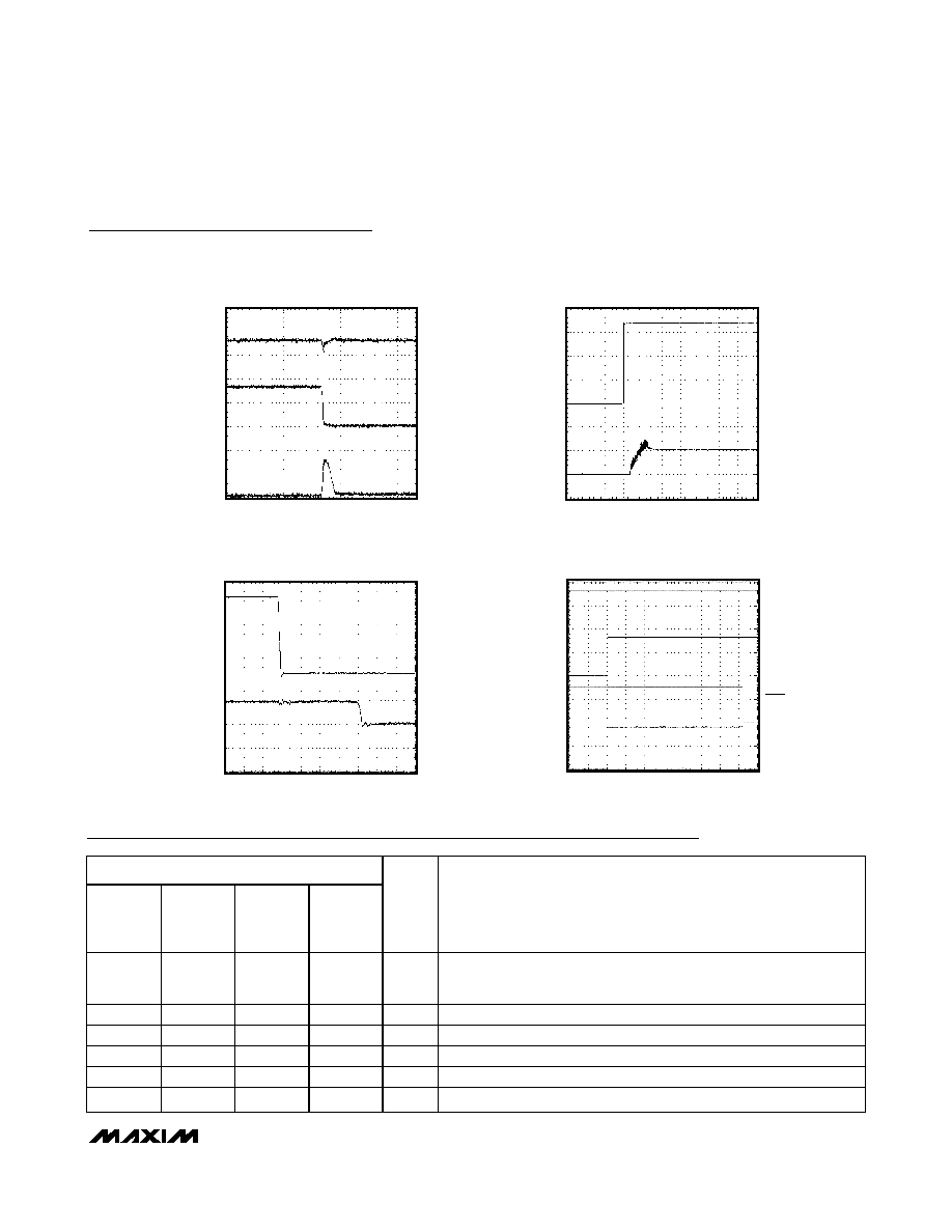
SWITCH TURN-ON TIME RESPONSE
MAX4789 toc14
100
µs/div
V
ON
1V/div
I
OUT
10mA/div
CURRENT-LIMIT RESPONSE
(OUT SHORTED TO GND)
MAX4789 toc13
40
µs/div
V
IN
2V/div
V
OUT
2V/div
I
OUT
5A/div
C
IN
= 1
µF
C
OUT
= 1
µF
Typical Operating Characteristics (continued)
(V
IN
= 3.3V, T
A
= +25°C, unless otherwise noted.)
PIN
TDFN
MAX4789
MAX4791
MAX4793
TDFN
MAX4790
MAX4792
MAX4794
5-SOT23
MAX4789
MAX4791
MAX4793
4-SOT143
MAX4789
MAX4794
NAME
FUNCTION
1
--
4
--
FLAG
Fault Output. This open-drain output goes low when the device stays in
forward or reverse current limit for more than the blanking time period.
FLAG is high impedance when a fault is not present or when ON is low.
2
2
2
2
GND
Ground
3
3
3
3
ON
Active-High Switch On Input. A logic high turns the switch on.
4
1, 4
--
--
N.C.
No Connection. Not internally connected.
5
5
1
4
IN
Input. Bypass with a 0.1µF ceramic capacitor to ground.
6
6
5
1
OUT
Switch Output. Bypass with a 0.1µF ceramic capacitor to ground.
FLAG-BLANKING RESPONSE
MAX4789 toc16
4ms/div
FLAG
2V/div
I
OUT
100mA/div
V
IN
2V/div
V
ON
2V/div
SWITCH TURN-OFF TIME RESPONSE
MAX4789 toc15
200ns/div
V
ON
2V/div
I
OUT
10mA/div