 | –≠–ª–µ–∫—Ç—Ä–æ–Ω–Ω—ã–π –∫–æ–º–ø–æ–Ω–µ–Ω—Ç: MAX478CSA | –°–∫–∞—á–∞—Ç—å:  PDF PDF  ZIP ZIP |

For free samples & the latest literature: http://www.maxim-ic.com, or phone 1-800-998-8800.
For small orders, phone 1-800-835-8769.
MAX478/MAX479
17µA Max, Dual/Quad, Single-Supply,
Precision Op Amps
________________________________________________________________ Maxim Integrated Products
1
1
2
3
4
8
7
6
5
V+
OUTB
INB-
INB+
V-
INA+
INA-
OUTA
MAX478
DIP/SO
TOP VIEW
1
2
3
4
14
13
12
11
OUTD
IND-
IND+
V-
V+
INA+
INA-
OUTA
MAX479
DIP/SO
5
6
7
10
9
8
INC+
INC-
OUTC
OUTB
INB-
INB+
A
D
B
C
A
B
_________________Pin Configurations
V2
V1
R3
R1
R2
R2
R1
+5V
V
OUT
MICROPOWER, HIGH INPUT IMPEDANCE DIFFERENTIAL
AMPLIFIER WITH VARIABLE GAIN IN 8-PIN DIP/SO
1/2MAX478
1/2MAX478
V
OUT
= (V1-V2) (1 +
R1
+ 2
R1
)
R2 R3
__________Typical Operating Circuit
19-0127; Rev. 1; 11/98
_______________General Description
The MAX478 and MAX479 are dual and quad micro-
power, precision op amps available in 8-pin and 14-pin
DIP and small-outline packages, respectively. Both
devices feature an extremely low, 17µA max supply
current per op amp, 70µV max offset voltage, 2.2µV/∞C
max offset voltage drift (0.5µV/∞C typ), and 250pA max
input offset current.
The MAX478 and MAX479 operate from a single sup-
ply. The input voltage range includes ground, and the
output swings to within a few millivolts of ground, which
eliminates pull-down resistors and saves power.
Both devices are optimized for single 3V and 5V sup-
ply operation, with guaranteed specifications at each
supply voltage. Specifications for ±15V operation are
also provided.
_______________________Applications
Battery- or Solar-Powered Systems:
Portable Instrumentation
Remote Sensor Amplifier
Satellite Circuitry
Micropower Sample-and-Hold
Thermocouple Amplifier
Micropower Filters
Single Lithium Cell Powered Systems
___________________________Features
o
17µA Max Supply Current (MAX478A/MAX479A)
o
70µV Max Offset Voltage (MAX478A)
o
Single-Supply Operation:
Input Voltage Range Includes Ground
Output Swings to Ground While Sinking Current
No Pull-Down Resistors Required
o
Dual Op Amp in 8-Pin DIP/SO Package (MAX478)
Quad Op Amp in 14-Pin DIP/SO Package (MAX479)
o
250pA Max Input Offset Current
(MAX478A/MAX479A)
o
0.5µV/∞C Offset-Voltage Drift
o
Output Sources and Sinks 5mA Load Current
______________Ordering Information
PART
TEMP. RANGE
PIN-PACKAGE
MAX478
ACPA
0∞C to +70∞C
8 Plastic DIP
MAX478CPA
0∞C to +70∞C
8 Plastic DIP
MAX478CSA
0∞C to +70∞C
8 SO
MAX478C/D
0∞C to +70∞C
Dice*
MAX478EPA
-40∞C to +85∞C
8 Plastic DIP
MAX478ESA
-40∞C to +85∞C
8 SO
MAX479
ACPD
0∞C to +70∞C
14 Plastic DIP
MAX479CPD
0∞C to +70∞C
14 Plastic DIP
MAX479CSD
0∞C to +70∞C
14 SO
MAX479EPD
-40∞C to +85∞C
14 Plastic DIP
MAX479ESD
-40∞C to +85∞C
14 SO
* Dice are specified at T
A
= +25∞C, DC parameters only.

MAX478/MAX479
17µA Max, Dual/Quad, Single-Supply,
Precision Op Amps
2
_______________________________________________________________________________________
Supply Voltage . . . . . . . . . . . . . . . . . . . . . . . . . . . . . . . . . . . . . . . . . . . . . . ±22V
Differential Input Voltage . . . . . . . . . . . . . . . . . . . . . . . . . . . . . . . . . . . . ±30V
Input Voltage . . . . . . . . . . . . . . . . . . . Equal to Positive Supply Voltage
. . . . . . . . . . . . . . . . . . . . . . . . . . . . . . .
5V Below Negative Supply Voltage
Output Short-Circuit Duration. . . . . . . . . . . . . . . . . . . . . . . . . Continuous
Continuous Power Dissipation (T
A
= +70∞C):
8-Pin Plastic DIP (derate 9.09mW/∞C above +70∞C) . . . . . 727mW
14-Pin Plastic DIP (derate 10.00mW/∞C above +70∞C) . . 800mW
14-Pin Wide SO (derate 9.52mW/∞C above +70∞C) . . . 762mW
Operating Temperature Ranges:
MAX47_ACP_/C_ _ . . . . . . . . . . . . . . . . . . . . . . . . . . . . . . . 0∞C to +70∞C
MAX47_E_ _ . . . . . . . . . . . . . . . . . . . . . . . . . . . . . . . . . . . . -40∞C to +85∞C
Storage Temperature Range . . . . . . . . . . . . . . . . . . . -65∞C to +150∞C
Lead Temperature (soldering, 10sec). . . . . . . . . . . . . . . . . . . . +300∞C
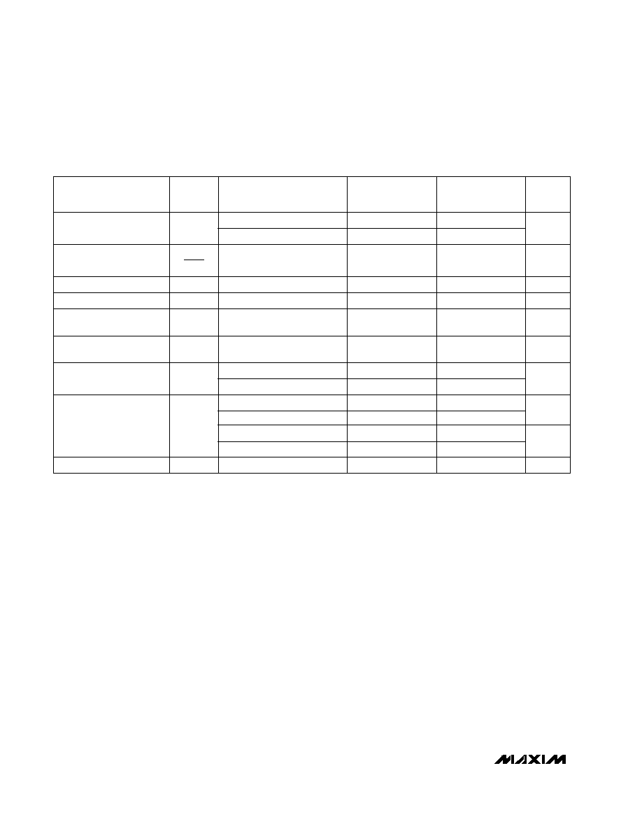
ELECTRICAL CHARACTERISTICS: 5V
(V
S
= 5V, 0V, V
CM
= 0.1V, V
O
= 1.4V, T
A
= +25∞C, unless otherwise noted.)
Stresses beyond those listed under "Absolute Maximum Ratings" may cause permanent damage to the device. These are stress ratings only, and functional
operation of the device at these or any other conditions beyond those indicated in the operational sections of the specifications is not implied. Exposure to
absolute maximum rating conditions for extended periods may affect device reliability.
ABSOLUTE MAXIMUM RATINGS
PARAMETER
SYMBOL
CONDITIONS
MAX478C/E
MAX479C/E
MIN
TYP
MAX
UNITS
Input Offset Voltage
V
OS
MAX478ACP/CP/EP
30
70
40
120
µV
MAX479ACP/CP/EP
35
100
40
150
MAX478CS/ES
80
180
MAX479CS/ES
90
250
V
OS
Time
0.5
0.6
µV/Mo.
I
OS
0.05
0.25
0.05
0.35
nA
Input Bias Current
I
B
3
5
3
6
nA
Input Noise Voltage
e
n
0.1Hz to 10Hz (Note 1)
0.9
2.0
0.9
µV
p-p
Input Noise Voltage
Density
fo = 10Hz (Note 1)
50
75
50
nV/
Hz
fo = 1000Hz (Note 1)
49
65
49
Input Noise Current
i
n
0.1Hz to 10Hz (Note 1)
1.5
2.5
1.5
pA
p-p
Input Noise Current
Density
fo = 10Hz (Note 1)
0.03
pA/
Hz
fo = 1000Hz
0.01
0.01
Input Resistance
R
IN
Differential mode (Note 1)
0.8
2.0
0.6
2.0
G
Common mode
12
12
Input Voltage Range
V
IN (CM)
Upper limit
3.5
3.9
3.5
3.9
V
Lower limit
0
-0.3
0
-0.3
CMRR
V
CM
= 0V to 3.5V
93
103
90
102
dB
Power-Supply
Rejection Ratio
PSRR
V
S
= 2.2V to 12V
94
104
92
104
dB
Large-Signal Voltage Gain
A
VOL
140
700
110
700
V/mV
V
O
= 0.03V to 3.5V, R
L
= 50k
80
200
70
200
MAX478AC
MAX479AC
MIN
TYP
MAX
Long-Term Input Offset-
Voltage Stability
Input Offset Current
Common-Mode
Rejection Ratio
V
O
= 0.03V to 4V, no load
(Note 1)
0.03
0.07

MAX478/MAX479
17µA Max, Dual/Quad, Single-Supply,
Precision Op Amps
_______________________________________________________________________________________
3
PARAMETER
SYMBOL
CONDITIONS
MAX478AC
MAX479AC
MIN
TYP
MAX
MAX478C/E
MAX479C/E
MIN
TYP
MAX
UNITS
Output Voltage Swing
V
OUT
Output low, no load
6.5
9.0
6.5
9.0
mV
Output low, 2k
to GND
0.2
0.6
0.2
0.6
Output low, I
SINK
= 100µA
120
160
120
160
4.2
4.4
V
Output high, 2k
to GND
3.5
3.8
3.5
3.8
Slew Rate
SR
A
V
= +1, C
L
= 1pF (Note 1)
0.013 0.025
0.013 0.025
V/µs
Gain-Bandwidth Product
GBW
f
O
5kHz
60
60
kHz
Channel Separation
V
IN
= 3V, R
L
= 10k
130
130
dB
Minimum Supply Voltage
V
S
(Note 2)
2.0
2.2
2.0
2.2
V
I
S
13
18
14
21
µA
Supply Current per
Amplifier
V
S
= ±1.5V, V
O
= 0V
12
17
13
20
Output high, no load
ELECTRICAL CHARACTERISTICS: 5V (continued)
(V
S
= 5V, 0V, V
CM
= 0.1V, V
O
= 1.4V, T
A
= +25∞C, unless otherwise noted.)
4.2
4.4
ELECTRICAL CHARACTERISTICS: 5V
(V
S
= 5V, 0V, V
CM
= 0.1V, V
O
= 1.4V, T
A
= 0∞C to +70∞C, unless otherwise noted.)
PARAMETER
SYMBOL
CONDITIONS
MAX478AC
MAX479AC
MIN
TYP
MAX
MAX478C
MAX479C
MIN
TYP
MAX
UNITS
MAX479CS
130
400
Input Offset Voltage
V
OS
MAX478ACP/CP
50
170
65
250
µV
MAX479ACP/CP
60
200
70
290
MAX478CS
120
300
Input Offset Voltage Drift
V
OS
T
MAX47_ACP/CP (Note 1)
0.5
2.2
0.6
3.0
µV/∞C
MAX47_CS (Note 1)
0.8
4.5
Input Offset Current
I
OS
0.06
0.35
0.06
0.50
nA
Input Bias Current
I
B
3
6
3
7
nA
CMRR
V
CM
= 0V to 3.4V
90
101
86
100
dB
Power-Supply
Rejection Ratio
PSRR
V
S
= 2.5V to 12V
90
102
88
102
dB
Large-Signal
Voltage Gain
A
VOL
105
500
80
500
V/mV
55
160
45
160
Output Voltage Swing
V
OUT
Output low, no load
8
11
8
11
mV
Output low, I
SINK
= 100µA
140
190
140
190
Output high, no load
4.1
4.3
4.1
4.3
V
Output high, 2k
to GND
3.3
3.8
3.3
3.8
Supply Current per Amplifier
I
S
14
21
15
24
µA
Common-Mode
Rejection Ratio
V
O
= 0.05V to 4V, no load (Note 1)
V
O
= 0.05V to 3.5V, R
L
= 50k
MAX478/MAX479
17µA Max, Dual/Quad, Single-Supply,
Precision Op Amps
4
_______________________________________________________________________________________
ELECTRICAL CHARACTERISTICS: 5V
(V
S
= 5V, 0V, V
CM
= 0.1V, V
O
= 1.4V, T
A
= -40∞C to +85∞C, unless otherwise noted.)
PARAMETER
SYMBOL
CONDITIONS
MAX478EP
MAX479EP
MIN
TYP
MAX
MAX478ES
MAX479ES
MIN
TYP
MAX
UNITS
Input Offset Voltage Drift
V
OS
T
(Note 1)
0.6
3.0
0.8
4.5
µV/∞C
Input Offset Current
I
OS
0.07
0.7
0.07
0.7
nA
Input Bias Current
I
B
4
8
4
8
nA
Common-Mode
Rejection Ratio
CMRR
V
CM
= 0.05V to 3.2V
84
98
84
98
dB
Input Offset Voltage
V
OS
MAX478
80
315
150
400
µV
Power-Supply
Rejection Ratio
PSRR
V
S
= 3.0V to 12V
86
100
86
100
dB
Large-Signal
Voltage Gain
A
VOL
V
O
= 0.05V to 4V, no load (Note 1)
55
350
55
350
V/mV
MAX479
80
345
160
530
V
O
= 0.05V to 3.5V, R
L
= 50k
35
130
35
130
Output Voltage Swing
V
OUT
Output low, no load
9
13
9
13
mV
Output low, I
SINK
= 100µA
160
220
160
220
Output high, no load
3.9
4.2
3.9
4.2
V
Output high, 2k
to GND
3.0
3.7
3.0
3.7
Supply Current per Amplifier
I
S
15
27
15
27
µA

MAX478/MAX479
17µA Max, Dual/Quad, Single-Supply,
Precision Op Amps
_______________________________________________________________________________________
5
ELECTRICAL CHARACTERISTICS: 3V
(V
S
= 3V, 0V, V
CM
= 0.1V, V
O
= 0.8V, T
A
= +25∞C, unless otherwise noted.)
PARAMETER
SYMBOL
CONDITIONS
MAX478AC
MAX479AC
MIN
TYP
MAX
MAX478C/E
MAX479C/E
MIN
TYP
MAX
UNITS
MAX479CS/ES
Input Offset Current
I
OS
90
270
0.05
0.05
nA
Input Bias Current
I
B
3
3
nA
Common-Mode
Rejection Ratio
CMRR
V
CM
= 0V to 1.7V
93
103
90
102
dB
Input Offset Voltage
V
OS
MAX478ACP/CP/EP
30
90
40
140
µV
MAX479ACP/CP/EP
35
120
40
170
Power-Supply
Rejection Ratio
PSRR
V
S
= 2.2V to 12V
94
104
92
104
dB
Large-Signal
Voltage Gain
A
VOL
100
600
100
600
V/mV
MAX478CS/ES
80
200
V
O
= 0.03V to 1.5V, R
L
= 50k
30
180
30
180
Output Voltage Swing
V
OUT
Output low, no load
6
9
6
9
mV
Output low, 2k
to GND
0.2
0.6
0.2
0.6
Output high, no load
2.2
2.4
2.2
2.4
V
Output high, 2k
to GND
1.8
2.0
1.8
2.0
Supply Current per Amplifier
I
S
12
17
13
20
µA
Input Noise Voltage
e
N
0.1Hz to 10Hz
1.0
1.0
µV
p-p
Input Voltage Range
V
IN (CM)
Upper limit
1.7
1.9
1.7
1.9
V
Lower limit
0
-0.3
Gain-Bandwidth Product
GBW
f
O
5kHz
50
50
kHz
Minimum Supply Voltage
V
S
2.2
2.2
V
V
O
= 0.03V to 2V, no load
(Note 1)
0
-0.3
With 300µV V
OS
degradation
1.7
1.7