 | ÐлекÑÑоннÑй компоненÑ: MAX5181 | СкаÑаÑÑ:  PDF PDF  ZIP ZIP |
Äîêóìåíòàöèÿ è îïèñàíèÿ www.docs.chipfind.ru
For free samples & the latest literature: http://www.maxim-ic.com, or phone 1-800-998-8800.
For small orders, phone 1-800-835-8769.
General Description
The MAX5181 is a 10-bit, current-output digital-to-ana-
log converter (DAC) designed for superior performance
in signal reconstruction or arbitrary waveform genera-
tion applications requiring analog signal reconstruction
with low distortion and low-power operation. The
MAX5184 provides equal specifications, with on-chip
precision resistors for voltage-output operation. The
MAX5181/MAX5184 are designed for a 10pVs glitch
operation to minimize unwanted spurious signal com-
ponents at the output. An on-board +1.2V bandgap cir-
cuit provides a well-regulated, low-noise reference that
can be disabled for external reference operation.
The devices are designed to provide a high level of sig-
nal integrity for the least amount of power dissipation.
They operate from a single +2.7V to +3.3V supply.
Additionally, these DACs have three modes of opera-
tion: normal, low-power standby, and full shutdown,
which provides the lowest possible power dissipation
with a 1µA max shutdown current. A fast wake-up time
(0.5µs) from standby mode to full DAC operation facili-
tates power conservation by activating the DAC only
when required.
The MAX5181/MAX5184 are available in 24-pin QSOP
packages and are specified for the extended (-40°C to
+85°C) temperature range. For lower resolution, 8-bit
versions, refer to the MAX5187/MAX5190 data sheet.
Applications
Signal Reconstruction
Arbitrary Waveform Generators (AWGs)
Direct Digital Synthesis
Imaging Applications
Features
o +2.7V to +3.3V Single-Supply Operation
o Wide Spurious-Free Dynamic Range: 70dB
at f
OUT
= 2.2MHz
o Fully Differential Output
o Low-Current Standby or Full Shutdown Modes
o Internal +1.2V, Low-Noise Bandgap Reference
o Small 24-Pin QSOP Package
10-Bit, 40MHz, Current/Voltage-Output DACs
________________________________________________________________ Maxim Integrated Products
1
24
23
22
21
20
19
18
17
1
2
3
4
5
6
7
8
REFO
REFR
DGND
DV
DD
AGND
OUTN
OUTP
CREF
TOP VIEW
D9
D8
D7
D6
CS
PD
DACEN
AV
DD
16
15
14
13
9
10
11
12
D5
D4
D3
D2
D1
DO
REN
CLK
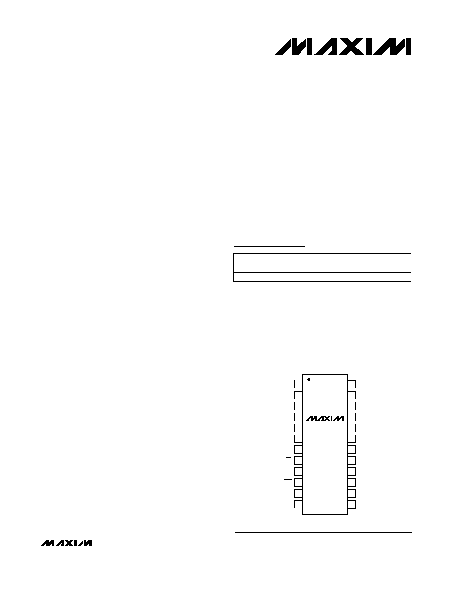
QSOP
MAX5181
MAX5184
19-1579; Rev 0; 12/99
PART
MAX5181BEEG
-40°C to +85°C
TEMP. RANGE
PIN-PACKAGE
24 QSOP
Pin Configuration
Ordering Information
MAX5184BEEG
-40°C to +85°C
24 QSOP
MAX5181/MAX5184
MAX5181/MAX5184
10-Bit, 40MHz, Current/Voltage-Output DACs
2
_______________________________________________________________________________________
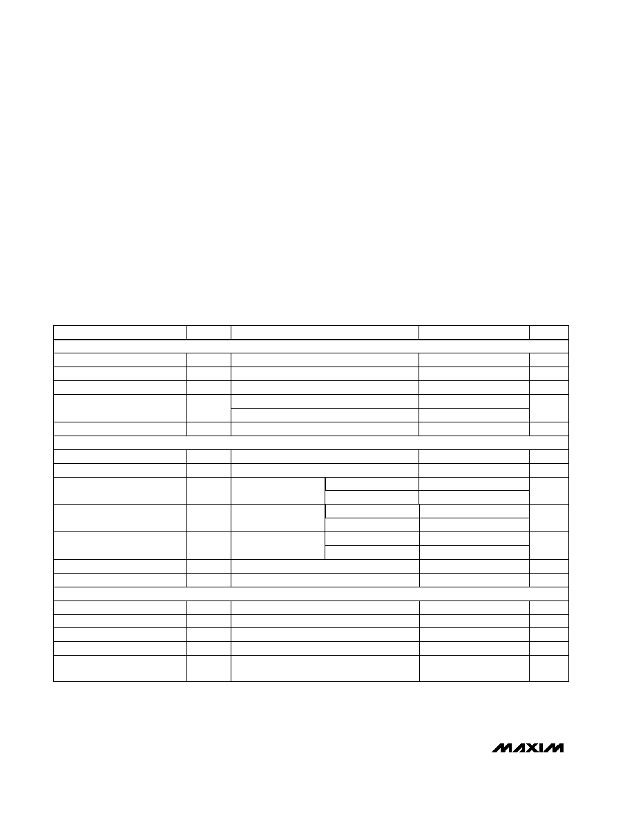
ABSOLUTE MAXIMUM RATINGS
ELECTRICAL CHARACTERISTICS
(AV
DD
= DV
DD
= +3V ±10%, AGND = DGND = 0, f
CLK
= 40MHz, I
FS
= 1mA, 400
differential output, C
L
= 5pF, T
A
= T
MIN
to T
MAX
,
unless otherwise noted. Typical values are at T
A
= +25°C.)
Stresses beyond those listed under "Absolute Maximum Ratings" may cause permanent damage to the device. These are stress ratings only, and functional
operation of the device at these or any other conditions beyond those indicated in the operational sections of the specifications is not implied. Exposure to
absolute maximum rating conditions for extended periods may affect device reliability.
AV
DD
, DV
DD
to AGND, DGND .................................-0.3V to +6V
Digital Inputs to DGND.............................................-0.3V to +6V
OUTP, OUTN, CREF to AGND .................................-0.3V to +6V
V
REF
to AGND ..........................................................-0.3V to +6V
AGND to DGND.....................................................-0.3V to +0.3V
AV
DD
to DV
DD
.................................................................... ±3.3V
Maximum Current into Any Pin............................................50mA
Continuous Power Dissipation (T
A
= +70°C)
24-Pin QSOP (derate 9.50mW/°C above +70°C) ........762mW
Operating Temperature Range
MAX518_BEEG ................................................-40°C to +85°C
Storage Temperature Range .............................-65°C to +150°C
Lead Temperature (soldering, 10sec) .............................+300°C
MAX5181 only
MAX5181 only
DACEN = 0, MAX5181 only
All 0s to all 1s
To ±0.5LSB error band
Guaranteed monotonic
MAX5181
(Note 1)
CONDITIONS
400
R
L
DAC External Output Resistor
Load
mA
0.5
1
1.5
I
FS
Full-Scale Output Current
µA
-1
1
Output Leakage Current
V
-0.3
0.8
Voltage Compliance of Output
mV
400
V
FS
Full-Scale Output Voltage
pA/
Hz
10
Output Noise
LSB
-2
±0.5
+2
INL
Integral Nonlinearity
Bits
10
N
Resolution
nVs
50
Clock and Data Feedthrough
dBc
72
SFDR
Spurious-Free Dynamic Range
to Nyquist
pVs
10
Glitch Impulse
ns
25
Output Settling Time
LSB
-1
±0.5
1
DNL
Differential Nonlinearity
-2
+2
Zero-Scale Error
LSB
-40
±15
+40
Full-Scale Error
UNITS
MIN
TYP
MAX
SYMBOL
PARAMETER
57
70
-68
-63
dB
-70
THD
Total Harmonic Distortion
to Nyquist
56
59
dB
61
SNR
Signal-to-Noise Ratio to Nyquist
f
OUT
= 550kHz
f
OUT
= 2.2MHz
f
OUT
= 550kHz
f
OUT
= 2.2MHz
f
OUT
= 550kHz
f
OUT
= 2.2MHz
f
CLK
= 40MHz
f
CLK
= 40MHz
f
CLK
= 40MHz
DYNAMIC PERFORMANCE
STATIC PERFORMANCE
ANALOG OUTPUT
MAX5184
-8
+8
LSB
MAX5181/MAX5184
10-Bit, 40MHz, Current/Voltage-Output DACs
_______________________________________________________________________________________
3
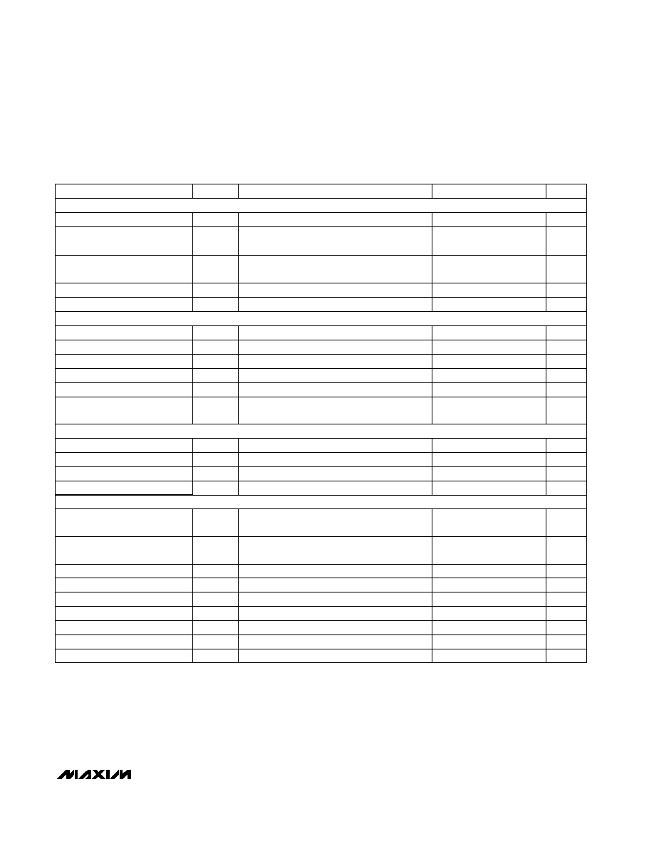
ELECTRICAL CHARACTERISTICS (continued)
(AV
DD
= DV
DD
= +3V ±10%, AGND = DGND = 0, f
CLK
= 40MHz, I
FS
= 1mA, 400
differential output, C
L
= 5pF, T
A
= T
MIN
to T
MAX
,
unless otherwise noted. Typical values are at T
A
= +25°C.)
Note 1: Excludes reference and reference resistor (MAX5184) tolerance.
TIMING CHARACTERISTICS
Output Voltage Temperature
Drift
TCV
REF
50
ppm/°C
Reference Supply Rejection
0.5
mV/V
Current Gain (I
FS
/ I
REF
)
8
mA/mA
PARAMETER
SYMBOL
MIN
TYP
MAX
UNITS
Digital Supply Current
I
DVDD
4.2
5.0
mA
Digital Power-Supply Voltage
DV
DD
2.7
3.3
V
Analog Supply Current
I
AVDD
1.7
4.0
mA
Analog Power-Supply Voltage
AV
DD
2.7
3.3
V
Standby Current
I
STANDBY
1.0
1.5
mA
Shutdown Current
I
SHDN
0.5
1
µA
Digital Input Voltage High
V
IH
2
V
Output Voltage Range
V
REF
1.12
1.2
1.28
V
Reference Output Drive
Capability
I
REFOUT
10
µA
Digital Input Voltage Low
V
IL
0.8
V
Digital Input Current
I
IN
±1
µA
Digital Input Capacitance
C
IN
10
pF
DAC DATA to CLK Rise Setup
Time
t
DS
10
ns
DAC CLK Rise to DATA Hold
Time
t
DH
0
ns
CS Fall to CLK Rise Time
5
ns
CS Fall to CLK Fall Time
5
ns
DACEN Rise Time to V
OUT
0.5
µs
PD Fall Time to V
OUT
50
µs
Clock Period
t
CLK
25
ns
Clock High Time
t
CH
10
ns
Clock Low Time
t
CL
10
ns
CONDITIONS
PD = 0, DACEN = 1, digital inputs at 0 or DV
DD
V
IN
= 0 or DV
DD
PD = 0, DACEN = 1, digital inputs at 0 or DV
DD
PD = 0, DACEN = 0, digital inputs at 0 or DV
DD
PD = 1, DACEN = X,
digital inputs at 0 or DV
DD
(X = don't care)
REFERENCE
POWER REQUIREMENTS
LOGIC INPUTS AND OUTPUTS
TIMING CHARACTERISTICS
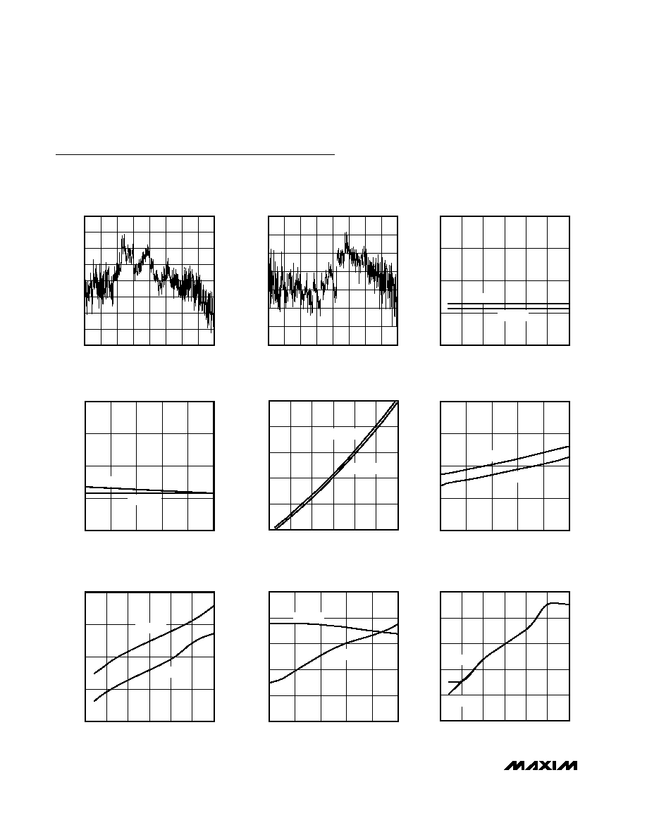
3.0
2.5
1.5
2.0
1.0
-40
35
-15
10
60
85
ANALOG SUPPLY CURRENT vs.
TEMPERATURE
MAX5181/4toc04
TEMPERATURE (
°C)
ANALOG SUPPLY CURRENT (mA)
MAX5181
MAX5184
8
7
6
5
4
3
2.5
4.0
3.0
3.5
4.5
5.0
5.5
DIGITAL SUPPLY CURRENT
vs. SUPPLY VOLTAGE
MAX5181/4toc05
SUPPLY VOLTAGE (V)
DIGITAL SUPPLY CURRENT (mA)
MAX5184
MAX5181
4.00
3.75
3.25
3.50
3.00
-40
35
-15
10
60
85
DIGITAL SUPPLY CURRENT vs.
TEMPERATURE
MAX5181/4toc06
TEMPERATURE (
°C)
DIGITAL SUPPLY CURRENT (mA)
MAX5184
MAX5181
610
600
590
580
570
2.5
4.0
3.0
3.5
4.5
5.0
5.5
STANDBY CURRENT vs.
SUPPLY VOLTAGE
MAX5181/4toc07
SUPPLY VOLTAGE (V)
STANDBY CURRENT (
µ
A)
MAX5184
MAX5181
600
590
570
560
580
550
-40
35
-15
10
60
85
STANDBY CURRENT vs.
TEMPERATURE
MAX5181/4toc08
TEMPERATURE (
°C)
STANDBY CURRENT (
µ
A)
MAX5184
MAX5181
0.14
0.12
0.10
0.06
0.08
0.04
2.5
4.0
3.0
3.5
4.5
5.0
5.5
SHUTDOWN CURRENT vs.
SUPPLY VOLTAGE
MAX5181/4toc09
SUPPLY VOLTAGE (V)
SHUTDOWN CURRENT (
µ
A)
MAX5184
MAX5181
MAX5181/MAX5184
10-Bit, 40MHz, Current/Voltage-Output DACs
4
_______________________________________________________________________________________
0.6
0.5
0.4
0.3
0.2
0.1
0
-0.1
-0.2
0
128
256
384 512
640 768
896 1024
INTEGRAL NONLINEARITY vs.
INPUT CODE
MAX5181/4toc01
INPUT CODE
INL (LSB)
0.4
0.3
0.2
0.1
0
-0.1
-0.2
-0.3
0
128
256
384 512
640 768
896 1024
DIFFERENTIAL NONLINEARITY vs.
INPUT CODE
MAX5181/4toc02
INPUT CODE
DNL (LSB)
3.0
2.5
2.0
1.5
1.0
2.5
4.0
3.0
3.5
4.5
5.0
5.5
ANALOG SUPPLY CURRENT
vs. SUPPLY VOLTAGE
MAX5181/4toc03
SUPPLY VOLTAGE (V)
ANALOG SUPPLY CURRENT (mA)
MAX5184
MAX5181
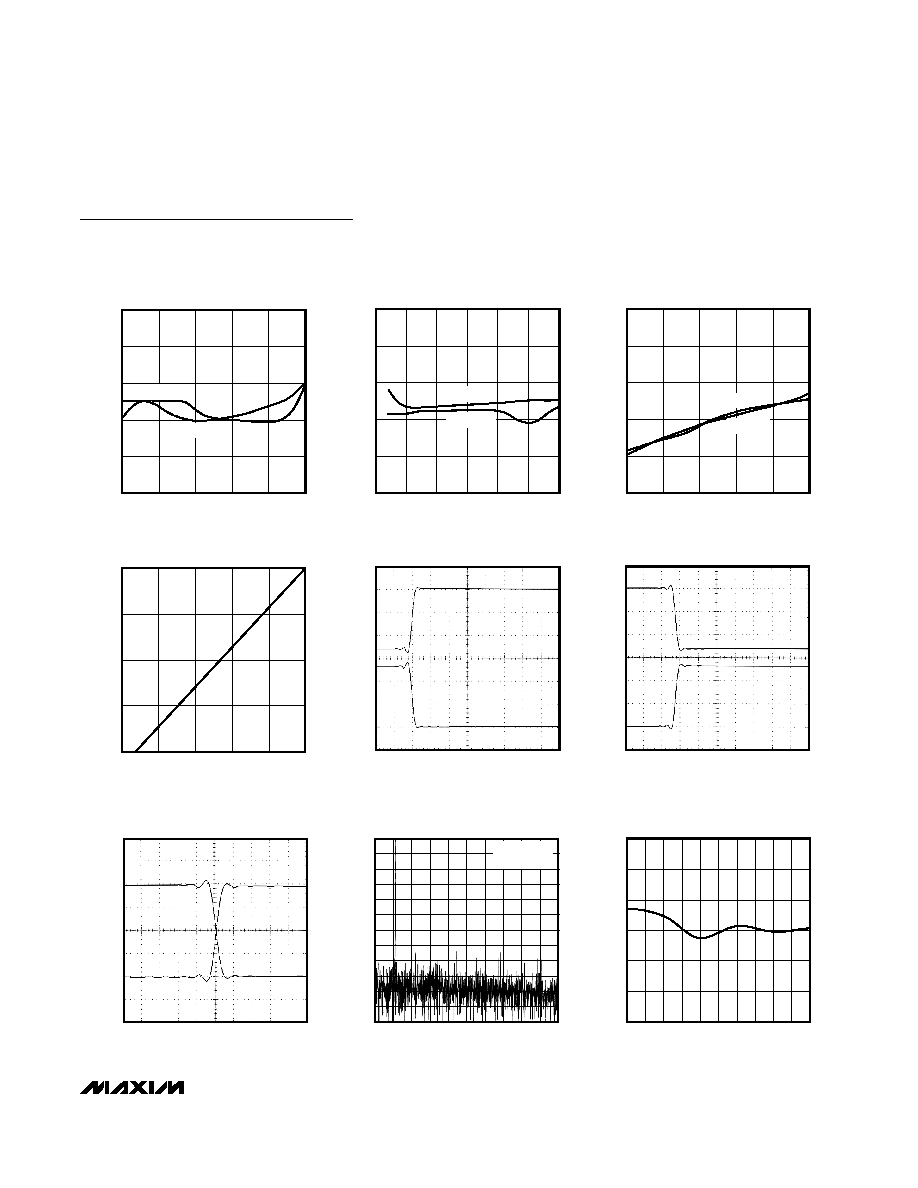
Typical Operating Characteristics
(AV
DD
= DV
DD
= +3V, AGND = DGND = 0, I
FS
= 1mA, 400
differential output, C
L
= 5pF, T
A
= +25°C, unless otherwise noted.)
MAX5181/MAX5184
10-Bit, 40MHz, Current/Voltage-Output DACs
_______________________________________________________________________________________
5
0.13
0.11
0.07
0.05
0.09
0.03
-40
35
-15
10
60
85
SHUTDOWN CURRENT vs.
TEMPERATURE
MAX5181/4toc10
TEMPERATURE (°C)
SHUTDOWN CURRENT (
µ
A)
MAX5184
MAX5181
1.28
1.27
1.26
1.25
1.24
1.23
2.5
4.0
3.0
3.5
4.5
5.0
5.5
INTERNAL REFERENCE VOLTAGE
vs. SUPPLY VOLTAGE
MAX5181/4toc11
SUPPLY VOLTAGE (V)
REFERENCE VOLTAGE (V)
MAX5184
MAX5181
1.28
1.27
1.25
1.24
1.26
1.23
-40
35
-15
10
60
85
INTERNAL REFERENCE VOLTAGE
vs. TEMPERATURE
MAX5181/4toc12
TEMPERATURE (
°C)
REFERENCE VOLTAGE (V)
MAX5184
MAX5181
Typical Operating Characteristics (continued)
(AV
DD
= DV
DD
= +3V, AGND = DGND = 0, I
FS
= 1mA, 400
differential output, C
L
= 5pF, T
A
= +25°C, unless otherwise noted.)
4.0
3.0
1.0
2.0
0
0
400
300
100
200
500
OUTPUT CURRENT vs.
REFERENCE CURRENT
MAX5181/4toc13
REFERENCE CURRENT (
µA)
OUTPUT CURRENT (mA)
DYNAMIC RESPONSE RISE TIME
MAX5181/4toc14
500ns/div
OUTP
150mV/
div
OUTN
150mV/
div
DYNAMIC RESPONSE FALL TIME
MAX5181/4toc15
500ns/div
OUTP
150mV/
div
OUTN
150mV/
div
SETTLING TIME
MAX5181/4toc16
12.5ns/div
OUTN
100mV/
div
OUTP
100mV/
div
0
-10
-20
-30
-40
-50
-60
-70
-80
-90
-100
-110
-120
0
2
4
6
8
10 12 14
16 18 20
FFT PLOT
MAX5181/4toc17
OUTPUT FREQUENCY (MHz)
(dBc)
f
OUT
= 2.2MHz
f
CLK
= 40MHz
100
90
70
60
50
80
40
10
20
25 30
35
40 45
50 55 60
15
SPURIOUS-FREE DYNAMIC RANGE
vs. CLOCK FREQUENCY
MAX5181/4toc18
CLOCK FREQUENCY (MHz)
SFDR (dBc)