 | ÐлекÑÑоннÑй компоненÑ: MAX5438 | СкаÑаÑÑ:  PDF PDF  ZIP ZIP |
MAX5436 DS
General Description
The MAX5436MAX5439 are 128-tap high-voltage (±5V
to ±15V) digital potentiometers in packages that are half
the size of comparable devices in 8-pin SO. They perform
the same function as mechanical potentiometers, but
replace the mechanics with a simple digital interface. The
digital logic is powered by a separate single +2.7V to
+5.25V supply voltage (V
CC
). The resistor string uses its
own analog supplies (V
DD
and V
SS
) that require
V
DD
- V
SS
to be greater than 9V and less than 31.5V. This
allows for greater flexibility in voltage ranges that can be
used with these devices. Examples of analog supply
ranges include not only dual voltages of ±5V to ±15V, but
single-supply voltages, such as +10V, +15V, +30V, -30V,
and more, as long as the ranges of V
DD
- V
SS
and V
CC
-
V
SS
are met.
The MAX5437/MAX5439 include an on-chip, high-
voltage, uncommitted amplifier, providing additional
reductions in board space and cost. Other features
include low 35ppm/°C end-to-end and 5ppm/°C ratio-
metric resistor temperature coefficients, a 3-wire SPITM/
QSPITM/MICROWIRETM-compatible serial interface, and
a power-on reset to midscale.
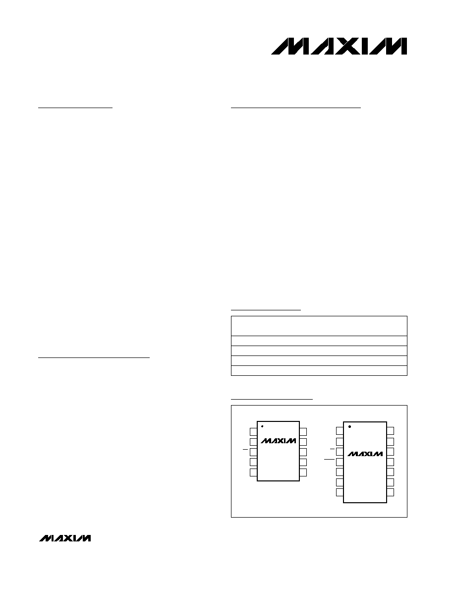
The MAX5436/MAX5438 are available in 10-pin µMAX
packages. The MAX5437/MAX5439 are available in 14-
pin TSSOP package. Each device is guaranteed over
the extended temperature range of -40°C to +85°C.
Applications
LCD Screen Contrast Adjustment
Data-Acquisition Systems
Mechanical Potentiometer Replacement
Low-Drift Programmable Gain Amplifier
Audio Volume Control
Features
o +10V to +30V Single-Supply Operation
o -28V to -10V Single Negative Supply Operation
o ±5V to ±15V Dual-Supply Operation
o 128 Tap Positions
o Uncommitted High-Voltage Amplifier
(MAX5437/MAX5439)
o Low Temperature Coefficient
35ppm/°C (End-to-End)
5ppm/°C (Ratiometric)
o Small-Footprint Packages
10-Pin µMAX (MAX5436/MAX5438)
14-Pin TSSOP (MAX5437/MAX5439)
o Glitchless Switching Between the Resistor Taps
o 3-Wire SPI/QSPI/MICROWIRE-Compatible Serial
Interface
o 50k/100k End-to-End Resistances
o Power-On Reset: Wiper Goes to Midscale
(Position 64)
MAX5436MAX5439
±15V, 128-Tap, Low-Drift Digital Potentiometers
________________________________________________________________ Maxim Integrated Products
1
1
2
3
4
5
10
9
8
7
6
V
CC
L
W
H
MAX5436/
MAX5438
µMAX
TOP VIEW
V
DD
14
13
12
11
10
9
8
1
2
3
4
5
6
7
MAX5437/
MAX5439
TSSOP
GND
CS
DIN
SCLK
V
SS
V
CC
L
W
H
SHDN
CS
DIN
SCLK
V
DD
IN+
IN-
OUT
V
SS
GND
Pin Configurations
Ordering Information
19-2657; Rev 0; 10/02
For pricing, delivery, and ordering information, please contact Maxim/Dallas Direct! at
1-888-629-4642, or visit Maxim's website at www.maxim-ic.com.
PART
TEMP RANGE
PIN-
PACKAGE
RESISTANCE
(k
)
MAX5436EUB
-40°C to +85°C 10 µMAX
50
MAX5437EUD
-40°C to +85°C 14 TSSOP
50
MAX5438EUB
-40°C to +85°C 10 µMAX
100
MAX5439EUD
-40°C to +85°C 14 TSSOP
100
SPI/QSPI are trademarks of Motorola, Inc.
MICROWIRE is a trademark of National Semiconductor Corp.
MAX5436MAX5439
±15V, 128-Tap, Low-Drift Digital Potentiometers
2
_______________________________________________________________________________________
ABSOLUTE MAXIMUM RATINGS
Stresses beyond those listed under "Absolute Maximum Ratings" may cause permanent damage to the device. These are stress ratings only, and functional
operation of the device at these or any other conditions beyond those indicated in the operational sections of the specifications is not implied. Exposure to
absolute maximum rating conditions for extended periods may affect device reliability.
V
DD
to GND, V
SS
= GND........................................-0.3V to +34V
V
SS
to GND, V
DD
= GND........................................-34V to +0.3V
V
DD
to V
SS
..............................................................-0.3V to +34V
V
DD
to V
CC
........................................................-6.3V to +28.75V
V
CC
to V
SS
..............................................................-0.3V to +34V
V
CC
to GND ..............................................................-0.3V to +6V
DIN, SCLK, CS, SHDN ...............................-0.3V to (V
CC
+ 0.3V)
H, L, W, IN+, IN-, OUT .....................(V
SS
- 0.3V) to (V
DD
+ 0.3V)
Maximum Continuous Current into H, L, and W
MAX5436MAX5439.......................................................±1mA
Continuous Power Dissipation (T
A
= +70°C)
10-Pin µMAX (derate 6.94mW/°C above +70°C) .........556mW
14-Pin TSSOP (derate 9.1mW/°C above +70°C) .........727mW
Operating Temperature Range ...........................-40°C to +85°C
Junction Temperature ......................................................+150°C
Storage Temperature Range .............................-65°C to +150°C
Lead Temperature (soldering, 10s) .................................+300°C
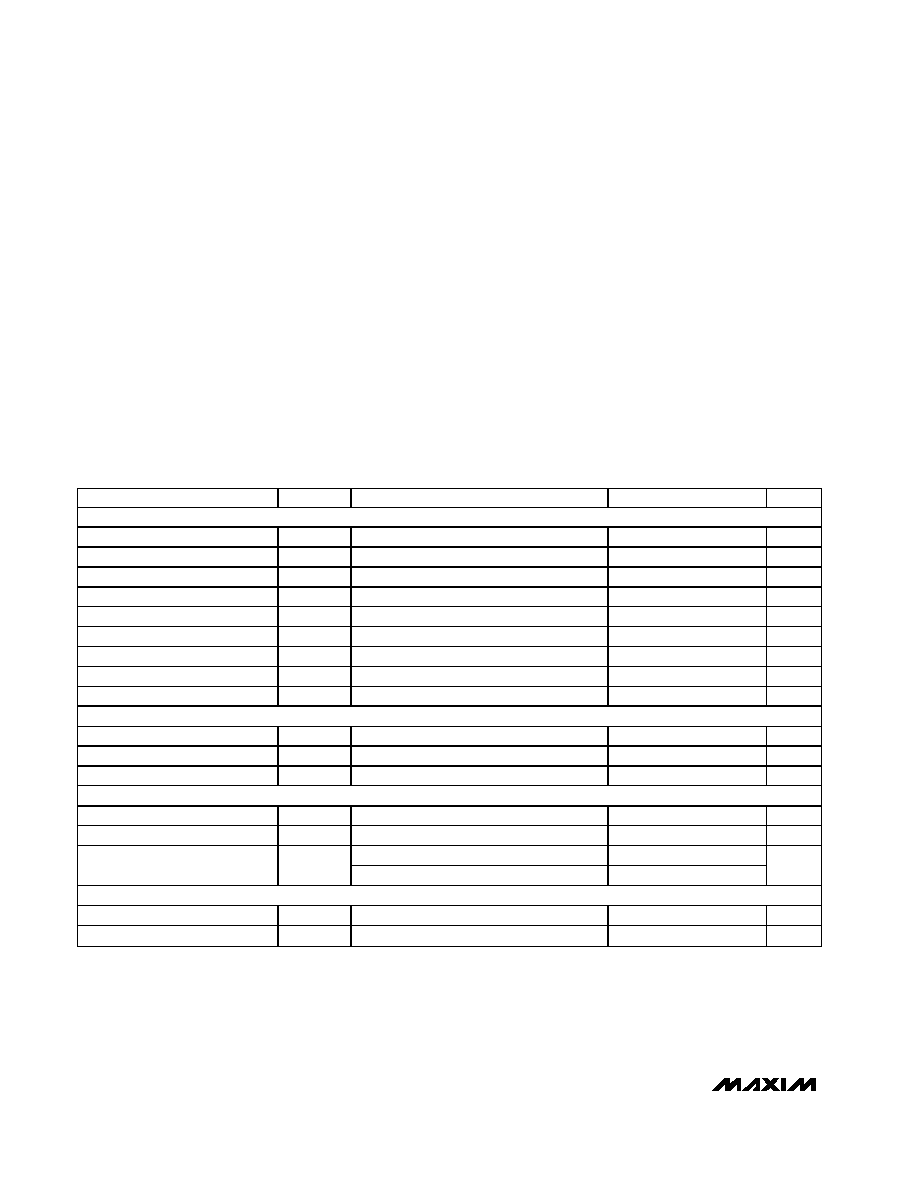
ELECTRICAL CHARACTERISTICS
(V
DD
= +15V, V
SS
= -15V, V
CC
= +5V, V
H
= V
DD
, V
L
= V
SS
, T
A
= -40°C to +85°C, unless otherwise noted. Typical values are at
T
A
= +25°C, unless otherwise noted.)
PARAMETER
SYMBOL
CONDITIONS
MIN
TYP
MAX
UNITS
DC PERFORMANCE (Voltage-Divider Mode)
Resolution
2
N
128
Taps
Integral Nonlinearity
INL
(Note 1)
±1
LSB
Differential Nonlinearity
DNL
(Note 1)
±1
LSB
End-to-End Resistor Tempco
TC
R
35
ppm/°C
Ratiometric Resistor Tempco
5
ppm/°C
Full-Scale Error
R
HL
= 50k
(MAX5436/MAX5438)
-0.3
LSB
Zero-Scale Error
R
HL
= 50k
(MAX5436/MAX5438)
+0.3
LSB
Full-Scale Error
R
HL
= 100k
(MAX5437/MAX5439)
-0.15
LSB
Zero-Scale Error
R
HL
= 100k
(MAX5437/MAX5439)
+0.15
LSB
DC PERFORMANCE (Variable-Resistor Mode)
Resolution
2
N
128
Taps
Integral Nonlinearity
INL
(Note 2)
±1
LSB
Differential Nonlinearity
DNL
(Note 2)
±1
LSB
DC PERFORMANCE (Resistor Characteristics)
Wiper Resistance
W
R
(Note 3)
0.9
2
k
Wiper Capacitance
W
C
Midscale
6
pF
MAX5437/MAX5439
75
100
125
End-to-End Resistance
R
HL
MAX5436/MAX5438
37.5
50
62.5
k
DIGITAL INPUTS
Input High Voltage
V
CC
= 4.75V to 5.25V (Note 4)
2.4
V
Input Low Voltage
V
CC
= 4.75V to 5.25V
0.8
V
MAX5436MAX5439
±15V, 128-Tap, Low-Drift Digital Potentiometers
_______________________________________________________________________________________
3
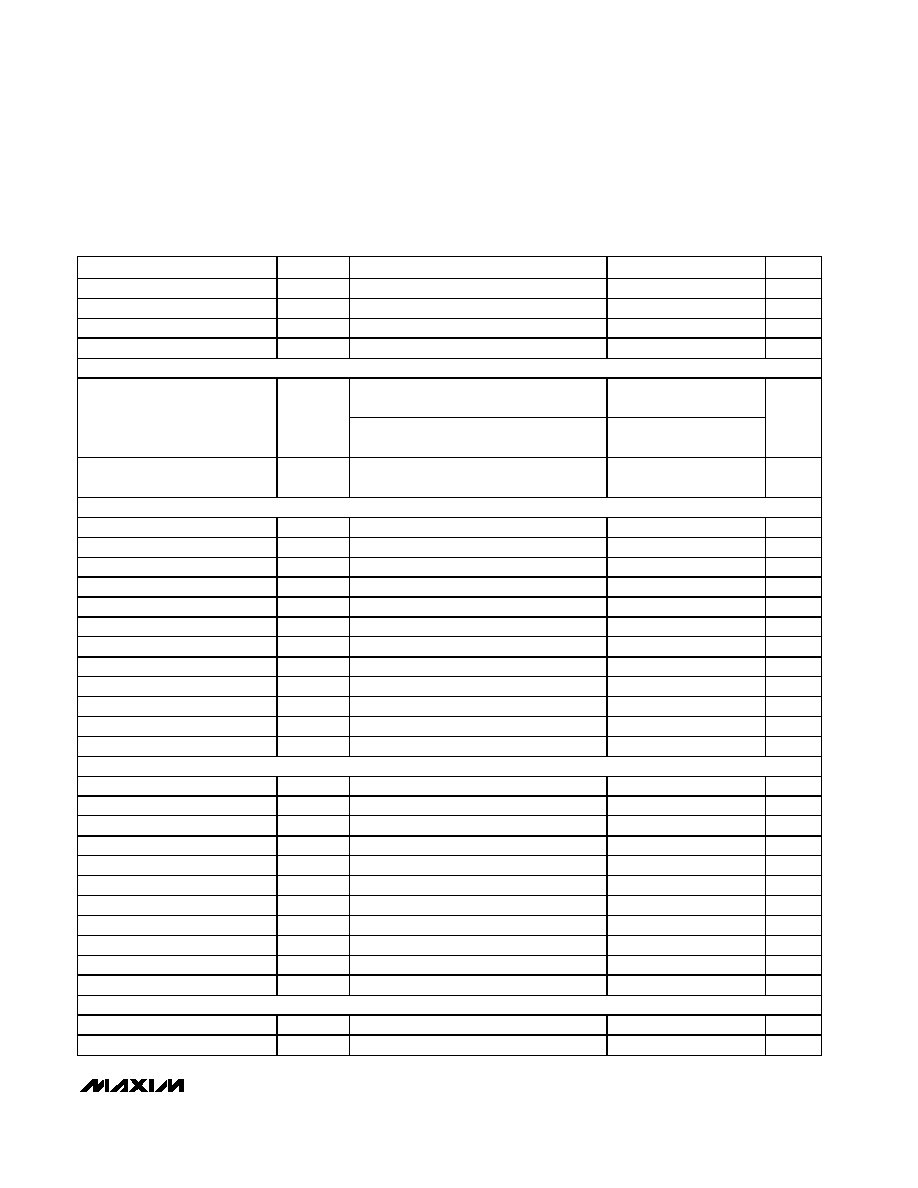
PARAMETER
SYMBOL
CONDITIONS
MIN
TYP
MAX
UNITS
Input High Voltage
V
CC
= 2.7V to 3.6V
2.0
V
Input Low Voltage
V
CC
= 2.7V to 3.6V
0.6
V
Input Leakage Current
±1.0
µA
Input Capacitance
5.0
pF
DYNAMIC CHARACTERISTICS (Analog)
R
HL
= 50k
, midscale, V
H
= 1.5V
P-P
,
C
WIPER
= 20pF, voltage-divider mode
400
Wiper -3dB Bandwidth
BW
W
R
HL
= 100k
, midscale, V
H
= 1.5V
P-P
,
C
WIPER
= 20pF, voltage-divider mode
200
kHz
Wiper Settling Time
t
IL
C
WIPER
= 20pF, code 1 to code 127, settle
to 0.5LSB
5
µs
AMPLIFIER CHARACTERISTICS (Analog)
Input Bias Current
I
B
15
nA
Input Offset Voltage
V
OS
±6
mV
Offset-Voltage Temperature Drift
V
OSD
10
µV/°C
Input Offset Current
I
OS
2
nA
Unity-Gain Bandwidth
UBW
A
C
LOAD
= 250pF
100
kHz
Slew Rate
SR
0.25
V/µs
Large-Signal Voltage Gain
A
VO
R
LOAD
= 100k
, V
OUT
=
±14V
100
V/mV
Input Noise
V
N
f = 1kHz
110
nV/
Hz
Input Compliance
CMR
I
V
SS
+ 1
V
DD
- 2
V
Output Compliance
CMR
O
I
LOAD
= ±5mA
V
SS
+ 1
V
DD
- 1
V
DC CMRR
CMRR
68
dB
DC PSRR
PSRR
70
dB
TIMING CHARACTERISTICS (Digital) (Note 5, Figure 3)
SCLK Clock Frequency
f
CLK
0
10
MHz
SCLK Clock Period
t
CP
100
ns
SCLK Pulse Width High
t
CH
40
ns
SCLK Pulse Width Low
t
CL
40
ns
CS Fall to SCLK Rise Setup Time
t
CSS
40
ns
SCLK Rise to CS Rise Hold Time
t
CSH
10
ns
DIN Setup Time
t
DS
40
ns
DIN Hold Time
t
DH
0
ns
SCLK Rise to CS Fall Delay
t
CSO
10
ns
CS Rise to SCLK Rise Hold
t
CS1
40
ns
CS Pulse Width High
t
CSW
100
ns
POWER SUPPLIES
Positive Analog Supply Voltage
V
DD
0
31.5
V
Negative Analog Supply Voltage
V
SS
-28.8
0
V
ELECTRICAL CHARACTERISTICS (continued)
(V
DD
= +15V, V
SS
= -15V, V
CC
= +5V, V
H
= V
DD
, V
L
= V
SS
, T
A
= -40°C to +85°C, unless otherwise noted. Typical values are at
T
A
= +25°C, unless otherwise noted.)
MAX5436MAX5439
±15V, 128-Tap, Low-Drift Digital Potentiometers
4
_______________________________________________________________________________________
ELECTRICAL CHARACTERISTICS (continued)
(V
DD
= +15V, V
SS
= -15V, V
CC
= +5V, V
H
= V
DD
, V
L
= V
SS
, T
A
= -40°C to +85°C, unless otherwise noted. Typical values are at
T
A
= +25°C, unless otherwise noted.)
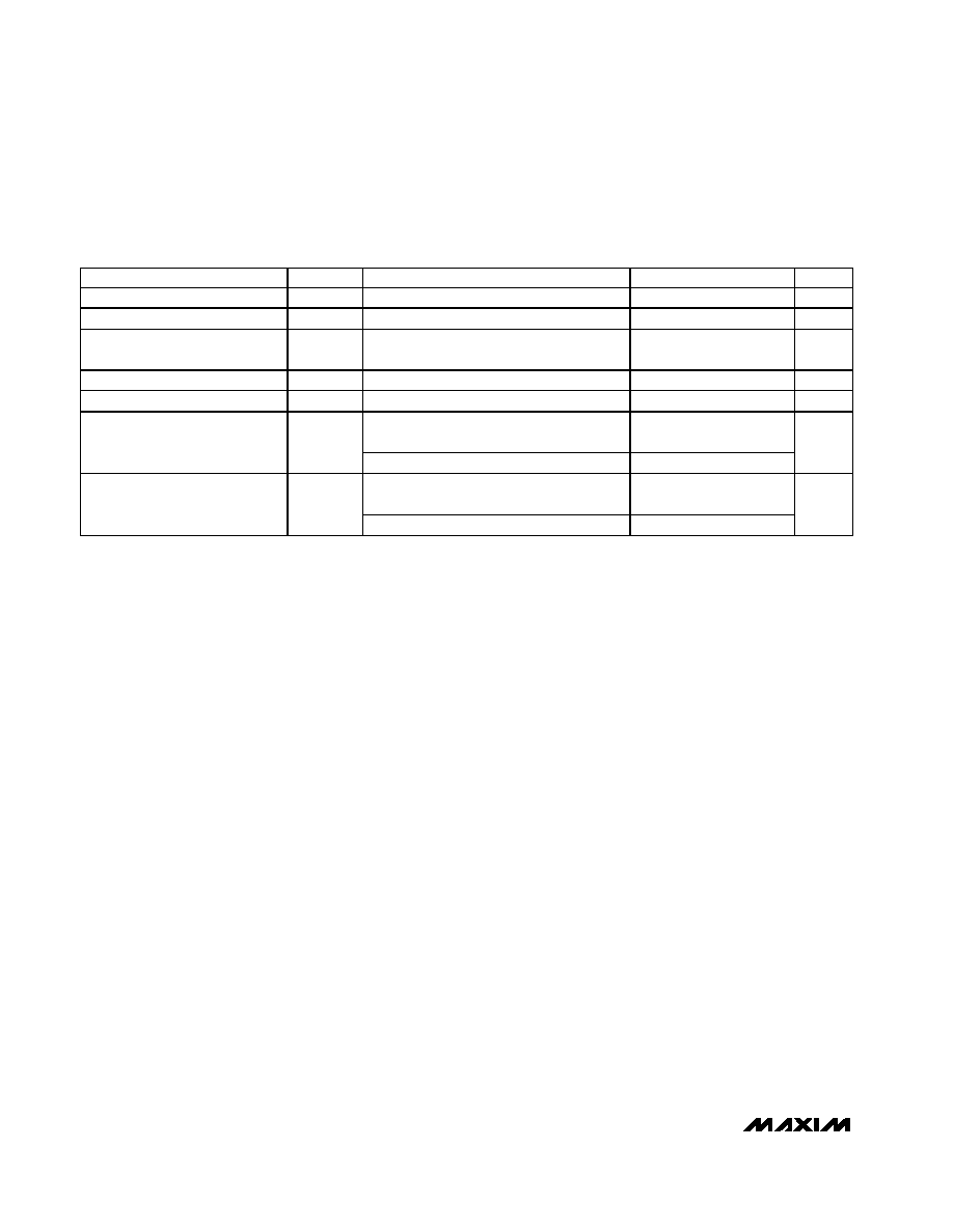
PARAMETER
SYMBOL
CONDITIONS
MIN
TYP
MAX
UNITS
Analog Supply Separation
V
DS
V
DD
- V
SS
9.0
31.5
V
Digital Supply Voltage
V
CC
2.70
5.25
V
Digital Supply to Negative Analog
Supply Separation
V
CS
V
CC
- V
SS
2.7
31.5
V
Power-On Reset Threshold
POR
1.6
V
Digital Supply Current
I
CC
(Note 4)
30
50
µA
MAX5436/MAX5438
SHDN = GND for MAX5437/MAX5439
30
60
Positive Analog Supply Current
I
DD
SHDN = V
CC
105
215
µA
MAX5436/MAX5438
SHDN = GND for MAX5437/MAX5439
55
110
Negative Analog Supply Current
I
SS
SHDN = V
CC
130
250
µA
Note 1: The DNL and INL are measured with the potentiometer configured as a voltage-divider with H = V
DD
and L = V
SS
. The
wiper terminal is unloaded.
Note 2: The DNL and INL are measured with the potentiometer configured as a variable resistor. H is unconnected and L = V
SS
.
The wiper terminal is driven with a source current of 80µA for the 50k
configuration and 40µA for the 100k configuration.
Note 3: The wiper resistance is measured assuming the source currents given in Note 2.
Note 4: Device draws current in excess of the specified supply current when a digital input is driven with a voltage of V
IN
< V
CC
-
0.6V or V
IN
> 0.5V. This is due to the CMOS input stage crowbar current. At V
IN
= 2.4V with V
CC
= 5.25V, this supply current
can be as high as 1.6mA.
Note 5: Guaranteed by design and characterization.
MAX5436MAX5439
±15V, 128-Tap, Low-Drift Digital Potentiometers
_______________________________________________________________________________________
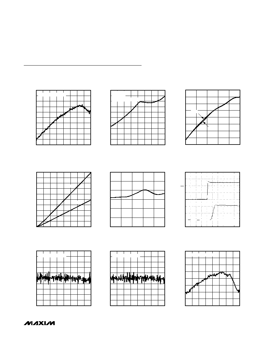
5
W-TO-L RESISTANCE CHANGE
vs. INPUT CODE
MAX5436 toc04
INPUT CODE
RESISTANCE (k
)
112
96
64
80
32
48
16
10
20
30
40
50
60
70
80
90
100
0
0
128
100k
50k
DIGITAL SUPPLY CURRENT
vs. TEMPERATURE
MAX5436 toc05
TEMPERATURE (
°C)
DIGITAL SUPPLY CURRENT (
µ
A)
60
35
10
-15
15
20
25
30
35
40
10
-40
85
MIDSCALE SWITCHING TRANSIENT
(CODE 63 TO CODE 64)
MAX5436 toc06
100ns/div
CS
2V/div
V
W-L
100mV/div
C
WIPER
= 20pF
VARIABLE-RESISTOR DNL
vs. INPUT CODE (50k
)
MAX5436 toc07
INPUT CODE
DNL (LSB)
112
96
64
80
32
48
16
-0.08
-0.06
-0.04
-0.02
0
0.02
0.04
0.06
0.08
0.10
-0.10
0
128
CONDITIONS OF NOTE 2
VARIABLE-RESISTOR DNL
vs. INPUT CODE (100k
)
MAX5436 toc08
INPUT CODE
DNL (LSB)
112
96
64
80
32
48
16
-0.08
-0.06
-0.04
-0.02
0
0.02
0.04
0.06
0.08
0.10
-0.10
0
128
CONDITIONS OF NOTE 2
-0.05
0
0.05
0.10
0.15
0.20
0.25
0.30
-0.10
VARIABLE-RESISTOR INL
vs. INPUT CODE (50k
)
MAX5436 toc09
INPUT CODE
INL (LSB)
112
96
64
80
32
48
16
0
128
CONDITIONS OF NOTE 2
Typical Operating Characteristics
(V
DD
= +15V, V
SS
= -15V, V
CC
= +5V, V
H
= V
DD
, V
L
= V
SS
, T
A
= +25°C, unless otherwise noted.)
WIPER RESISTANCE vs. INPUT CODE
MAX5436 toc01
INPUT CODE
RESISTANCE (
)
112
96
64
80
32
48
16
875
900
925
950
975
1000
1025
1050
1075
1100
850
0
128
CONDITIONS OF NOTE 2
WIPER RESISTANCE vs. INPUT CODE
MAX5436 toc02
INPUT CODE
RESISTANCE (
)
112
96
64
80
32
48
16
1200
1400
1600
1800
2000
2200
2400
2600
2800
3000
1000
0
128
V
DD
= +5V
V
SS
= -5V
CONDITIONS OF NOTE 2
END-TO-END RESISTANCE % CHANGE
vs. TEMPERATURE
MAX5436 toc03
TEMPERATURE (
°C)
END-TO-END RESISTANCE % CHANGE
60
35
-15
10
-0.20
-0.15
-0.10
-0.05
0
0.05
0.10
0.15
-0.25
-40
85
50k
100k