
General Description
The MAX6034 family of precision, low-dropout, microp-
ower voltage references are available in the miniature
3-pin SC70 surface-mount package. They feature a
proprietary temperature coefficient curvature-correction
circuit and laser-trimmed, thin-film resistors that result
in a low temperature coefficient of 30ppm/∞C (max) and
initial accuracy of ±0.20% (max). These devices are
available over the extended temperature range of -40∞C
to +85∞C.
The MAX6034 family of series-mode voltage references
typically draw only 90µA of supply current and can
source 1mA and sink 200µA of load current. Unlike
conventional shunt-mode (two terminal) references that
waste supply current and require an external resistor,
devices in the MAX6034 family offer supply current that
is virtually independent of supply voltage (16µA/V, max
variation) and do not require an external resistor. These
internally compensated devices do not require an
external compensation capacitor, but are stable with up
to 1µF of load capacitance. Eliminating the external
compensation capacitor saves valuable board space in
space-critical applications. The low dropout voltage
and supply-independent, ultra-low supply current make
the MAX6034 ideal for battery-powered applications.
Applications
Hand-Held Equipment
Data-Acquisition Systems
Industrial and Process Control Systems
Battery-Operated Equipment
Hard-Disk Drives
Features
o Ultra-Small, 3-Pin SC70 Package
o ±0.2% (max) Initial Accuracy
o 30ppm/∞C (max) Temperature Coefficient
o 90µA Supply Current
o 200mV (max) Dropout Voltage at 1mA Load
Current
o Stable with C
LOAD
= 0 to 1µF
o No Output Capacitor Needed
MAX6034
Precision, Micropower, Low-Dropout, SC70
Series Voltage Reference
________________________________________________________________ Maxim Integrated Products
1
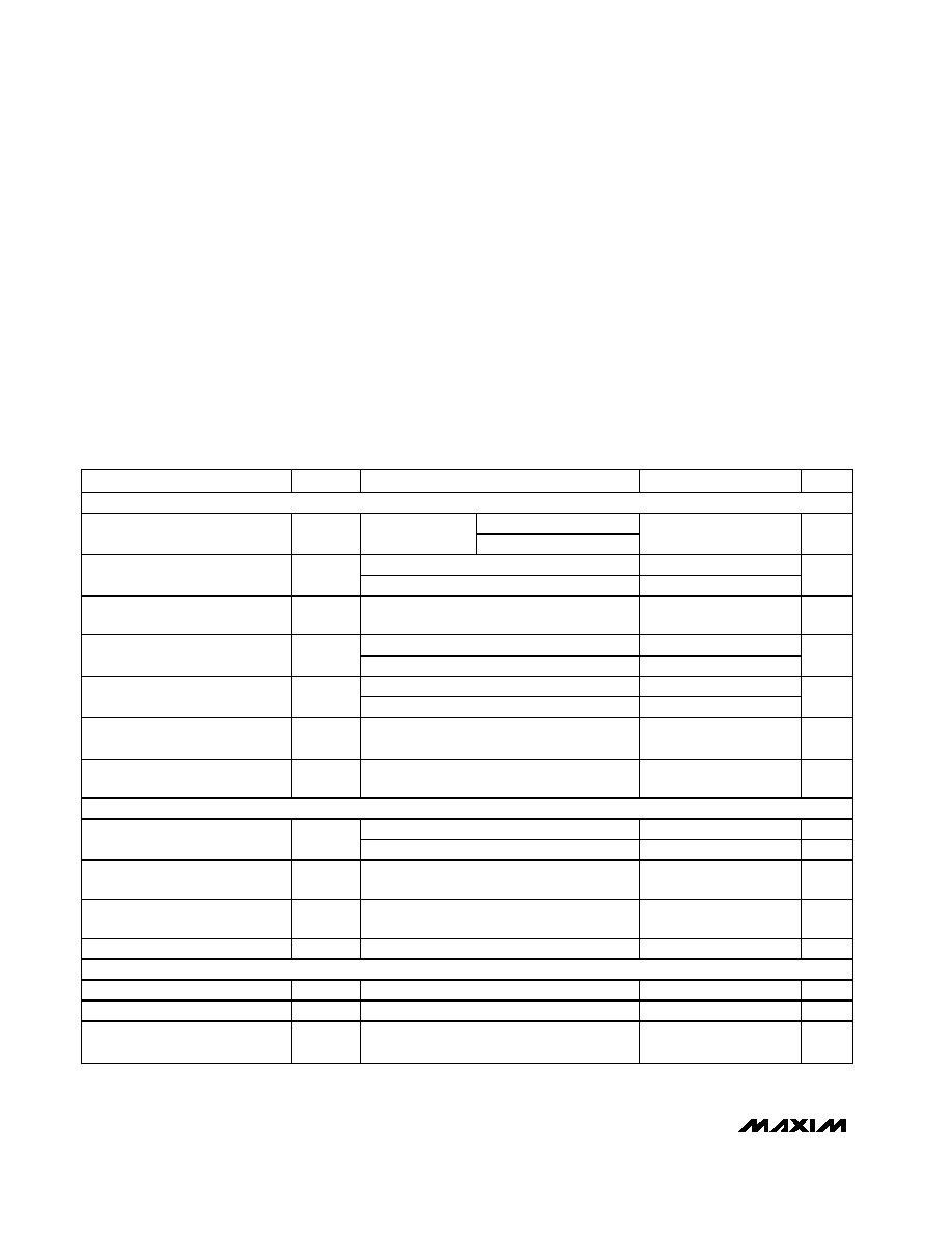
Ordering Information
19-2428; Rev 0; 4/02
For pricing, delivery, and ordering information, please contact Maxim/Dallas Direct! at
1-888-629-4642, or visit Maxim's website at www.maxim-ic.com.
PART
TEMP RANGE
PI N -
PA C K A G E
TOP
MARK
MAX6034AEXR21-T
-40∞C to +85∞C
3 SC70-3
AJH
MAX6034BEXR21-T
-40∞C to +85∞C
3 SC70-3
AJM
MAX6034AEXR25-T
-40∞C to +85∞C
3 SC70-3
AJI
MAX6034BEXR25-T
-40∞C to +85∞C
3 SC70-3
AJN
MAX6034AEXR30-T
-40∞C to +85∞C
3 SC70-3
AJJ
MAX6034BEXR30-T
-40∞C to +85∞C
3 SC70-3
AJO
MAX6034AEXR33-T
-40∞C to +85∞C
3 SC70-3
AJK
MAX6034BEXR33-T
-40∞C to +85∞C
3 SC70-3
AJP
MAX6034AEXR41-T
-40∞C to +85∞C
3 SC70-3
AJL
MAX6034BEXR41-T
-40∞C to +85∞C
3 SC70-3
AJQ
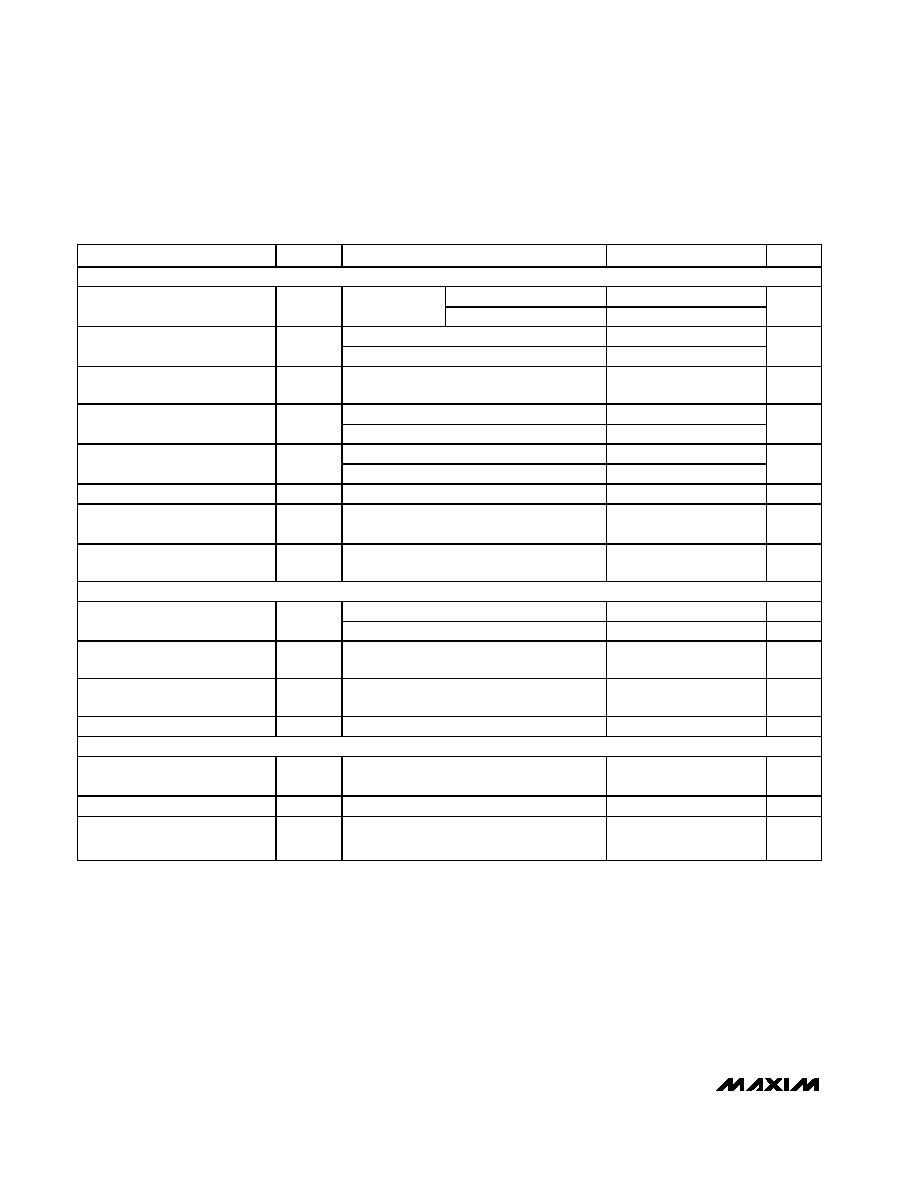
PART
V
OUT
INPUT VOLTAGE (V)
MAX6034_EXR21-T
2.048
2.5 to 5.5
MAX6034_EXR25-T
2.500
(V
OUT
+ 200mV) to 5.5
MAX6034_EXR30-T
3.000
(V
OUT
+ 200mV) to 5.5
MAX6034_EXR33-T
3.300
(V
OUT
+ 200mV) to 5.5
MAX6034_EXR41-T
4.096
(V
OUT
+ 200mV) to 5.5
Selector Guide
OUT
1
3
GND
IN
MAX6034
SC70
TOP VIEW
2
Pin Configuration
MAX6034
*
*CAPACITOR IS OPTIONAL.
REFERENCE
OUT
OUT
IN
GND
+SUPPLY INPUT (SEE SELECTOR GUIDE)
Typical Operating Circuit
MAX6034
Precision, Micropower, Low-Dropout, SC70
Series Voltage Reference
2
_______________________________________________________________________________________
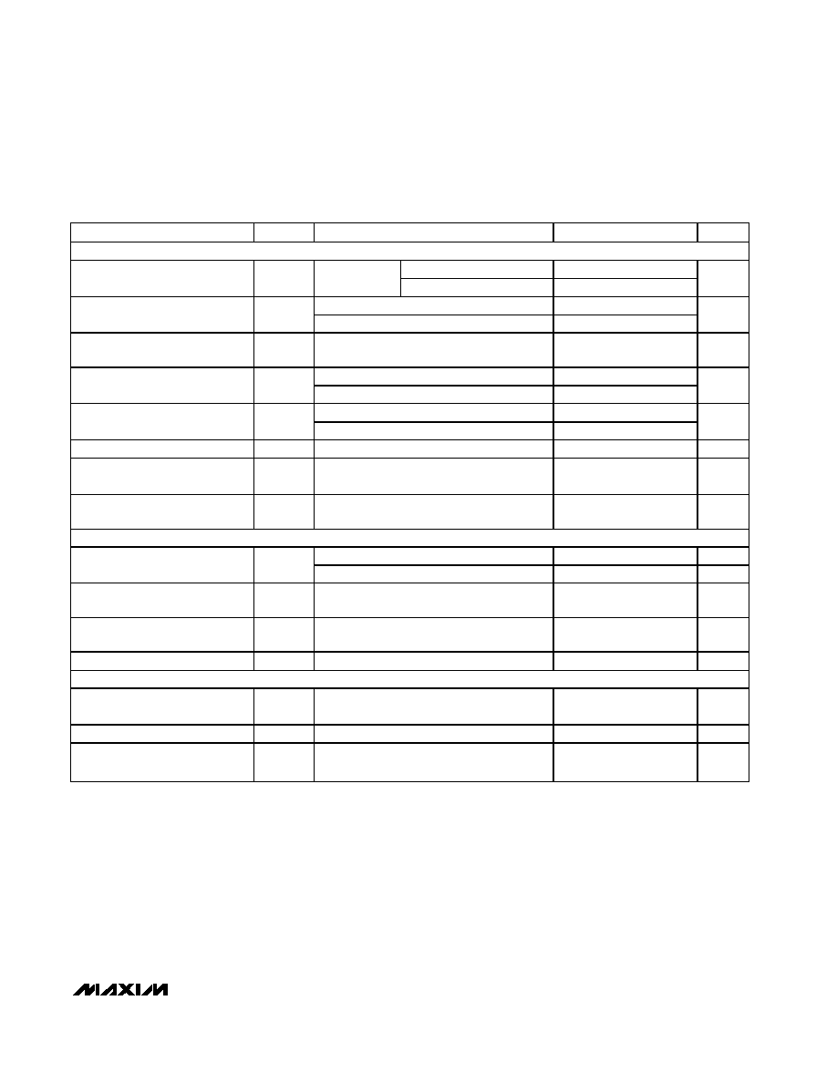
ABSOLUTE MAXIMUM RATINGS
ELECTRICAL CHARACTERISTICS≠MAX6034_21 (V
OUT
= 2.048V)
(V
IN
= 2.7V, I
OUT
= 0, T
A
= T
MIN
to T
MAX
, unless otherwise noted. Typical values are at T
A
= +25∞C.) (Note 1)
Stresses beyond those listed under "Absolute Maximum Ratings" may cause permanent damage to the device. These are stress ratings only, and functional
operation of the device at these or any other conditions beyond those indicated in the operational sections of the specifications is not implied. Exposure to
absolute maximum rating conditions for extended periods may affect device reliability.
(Voltages Referenced to GND)
IN ...........................................................................-0.3V to +6.0V
OUT .............................................................-0.3V to (V
IN
+ 0.3V)
Output Short Circuit to GND or IN..............................Continuous
Continuous Power Dissipation (T
A
= +70∞C)
3-Pin SC70 (derate 2.9mW/∞C above +70∞C) .............235mW
Operating Temperature Range ...........................-40∞C to +85∞C
Junction Temperature ......................................................+150∞C
Storage Temperature Range .............................-65∞C to +150∞C
Lead Temperature (soldering, 10s) ................................+300∞C
PARAMETER
SYMBOL
CONDITIONS
MIN
TYP
MAX
UNITS
OUTPUT
MAX6034A_21 (±0.2%)
2.044
2.048
2.052
Output Voltage
V
OUT
T
A
= +25∞C
MAX6034B_21 (±0.4%)
2.040
2.048
2.056
V
MAX6034A_21
7
30
Output Voltage Temperature
Coefficient (Note 2)
TCV
OUT
MAX6034B_21
7
75
ppm/∞C
Line Regulation
V
OUT
/
V
IN
2.5V
V
IN
5.5V
33
220
µV/V
Sourcing: 0
I
OUT
1mA
0.25
1.0
Load Regulation
V
OUT
/
I
OUT
Sinking: 0
I
OUT
200µA
2.1
62
mV/mA
Short to GND
12
OUT Short-Circuit Current
I
SC
Short to IN
4
mA
Temperature Hysteresis
V
OUT
/
cycle
(Note 3)
100
ppm
Long-Term Stability
V
OUT
/
time
1000hr at T
A
= +25∞C
90
ppm/
1000hr
DYNAMIC
f = 0.1Hz to 10Hz
45
µV
P-P
Noise Voltage
e
OUT
f = 10Hz to 10kHz
46
µV
RMS
Ripple Rejection
V
OUT
/
V
IN
V
IN
= 2.7V
±100mV, f = 120Hz
80
dB
Turn-On Settling Time
t
R
To V
OUT
= 0.1% of final value,
C
OUT
= 50pF
85
µs
Capacitive-Load Stability Range
C
OUT
(Note 4)
0
1
µF
INPUT
Supply Voltage Range
V
IN
Guaranteed by line-regulation test
2.5
5.5
V
Quiescent Supply Current
I
IN
85
115
µA
Change in Supply Current Per
Change in Input Voltage
I
IN
/
V
IN
2.5V
V
IN
5.5V
4.1
16
µA/V

MAX6034
Precision, Micropower, Low-Dropout, SC70
Series Voltage Reference
_______________________________________________________________________________________
3
ELECTRICAL CHARACTERISTICS≠MAX6034_25 (V
OUT
= 2.500V)
(V
IN
= 2.7V, I
OUT
= 0, T
A
= T
MIN
to T
MAX
, unless otherwise noted. Typical values are at T
A
= +25∞C.) (Note 1)
PARAMETER
SYMBOL
CONDITIONS
MIN
TYP
MAX
UNITS
OUTPUT
MAX6034A_25 (±0.2%)
2.495
2.500
2.505
Output Voltage
V
OUT
T
A
= +25∞C
MAX6034B_25 (±0.4%)
2.490
2.500
2.510
V
MAX6034A_25
7
30
Output Voltage Temperature
Coefficient (Note 2)
TCV
OUT
MAX6034B_25
7
75
ppm/∞C
Line Regulation
V
OUT
/
V
IN
(V
OUT
+ 200mV)
V
IN
5.5V
40
250
µV/V
Sourcing: 0
I
OUT
1mA
0.22
1.0
Load Regulation
V
OUT
/
I
OUT
Sinking: 0
I
OUT
200µA
2.5
8
mV/mA
Short to GND
12
OUT Short-Circuit Current
I
SC
Short to IN
4
mA
Dropout Voltage
V
IN
-
V
OUT
I
OUT
= 1mA (Note 5)
70
200
mV
Temperature Hysteresis
V
OUT
/
cycle
(Note 3)
100
ppm
Long-Term Stability
V
OUT
/
time
1000hr at T
A
= +25∞C
90
ppm/
1000hr
DYNAMIC
f = 0.1Hz to 10Hz
55
µV
P-P
Noise Voltage
e
OUT
f = 10Hz to 10kHz
64
µV
RMS
Ripple Rejection
V
OUT
/
V
IN
V
IN
= 2.7V
±100mV, f = 120Hz
80
dB
Turn-On Settling Time
t
R
To V
OUT
= 0.1% of final value,
C
OUT
= 50pF
140
µs
Capacitive-Load Stability Range
C
OUT
(Note 4)
0
1
µF
INPUT
Supply Voltage Range
V
IN
Guaranteed by line-regulation test
V
OUT
+ 0.2
5.5
V
Quiescent Supply Current
I
IN
85
115
µA
Change in Supply Current Per
Change in Input Voltage
I
IN
/
V
IN
(V
OUT
+ 200mV)
V
IN
5.5V
4.2
16
µA/V
MAX6034
Precision, Micropower, Low-Dropout, SC70
Series Voltage Reference
4
_______________________________________________________________________________________
ELECTRICAL CHARACTERISTICS≠MAX6034_30 (V
OUT
= 3.000V)
(V
IN
= 5V, I
OUT
= 0, T
A
= T
MIN
to T
MAX
, unless otherwise noted. Typical values are at T
A
= +25∞C.) (Note 1)
PARAMETER
SYMBOL
CONDITIONS
MIN
TYP
MAX
UNITS
OUTPUT
MAX6034A_30 (±0.2%)
2.994
3.000
3.006
Output Voltage
V
OUT
T
A
= +25∞C
MAX6034B_30 (±0.4%)
2.988
3.000
3.012
V
MAX6034A_30
7
30
Output Voltage Temperature
Coefficient (Note 2)
TCV
OUT
MAX6034B_30
7
75
ppm/∞C
Line Regulation
V
OUT
/
V
IN
(V
OUT
+ 200mV)
V
IN
5.5V
43
280
µV/V
Sourcing: 0
I
OUT
1mA
0.30
1.3
Load Regulation
V
OUT
/
I
OUT
Sinking: 0
I
OUT
200µA
2.6
8
mV/mA
Short to GND
13
OUT Short-Circuit Current
I
SC
Short to IN
4
mA
Dropout Voltage
V
IN
- V
OU T
I
OUT
= 1mA (Note 5)
70
200
mV
Temperature Hysteresis
V
OUT
/
cycle
(Note 3)
100
ppm
Long-Term Stability
V
OUT
/
time
1000hr at T
A
= +25∞C
90
ppm/
1000hr
DYNAMIC
f = 0.1Hz to 10Hz
66
µV
P-P
Noise Voltage
e
OUT
f = 10Hz to 10kHz
80
µV
RMS
Ripple Rejection
V
OUT
/
V
IN
V
IN
= 5V
±100mV, f = 120Hz
76
dB
Turn-On Settling Time
t
R
To V
OUT
= 0.1% of final value,
C
OUT
= 50pF
165
µs
Capacitive-Load Stability Range
C
OUT
(Note 4)
0
1
µF
INPUT
Supply Voltage Range
V
IN
Guaranteed by line-regulation test
V
OUT
+ 0.2
5.5
V
Quiescent Supply Current
I
IN
95
125
µA
Change in Supply Current Per
Change in Input Voltage
I
IN
/
V
IN
(V
OUT
+ 200mV)
V
IN
5.5V
4.5
16
µA/V
MAX6034
Precision, Micropower, Low-Dropout, SC70
Series Voltage Reference
_______________________________________________________________________________________
5
ELECTRICAL CHARACTERISTICS≠MAX6034_33 (V
OUT
= 3.300V)
(V
IN
= 5V, I
OUT
= 0, T
A
= T
MIN
to T
MAX
, unless otherwise noted. Typical values are at T
A
= +25∞C.) (Note 1)
PARAMETER
SYMBOL
CONDITIONS
MIN
TYP
MAX
UNITS
OUTPUT
MAX6034A_33 (±0.2%)
3.293
3.300
3.307
Output Voltage
V
OUT
T
A
= +25∞C
MAX6034B_33 (±0.4%)
3.287
3.300
3.313
V
MAX6034A_33
7
30
Output Voltage Temperature
Coefficient (Note 2)
TCV
OUT
MAX6034B_33
7
75
ppm/∞C
Line Regulation
V
OUT
/
V
IN
(V
OUT
+ 200mV)
V
IN
5.5V
45
300
µV/V
Sourcing: 0
I
OUT
1mA
0.3
1.3
Load Regulation
V
OUT
/
I
OUT
Sinking: 0
I
OUT
200µA
3
8.6
mV/mA
Short to GND
13
OUT Short-Circuit Current
I
SC
Short to IN
4
mA
Dropout Voltage
V
IN
- V
OU T
I
OUT
= 1mA (Note 5)
70
200
mV
Temperature Hysteresis
V
OUT
/
cycle
(Note 3)
100
ppm
Long-Term Stability
V
OUT
/
time
1000hr at T
A
= +25∞C
90
ppm/
1000hr
DYNAMIC
f = 0.1Hz to 10Hz
73
µV
P-P
Noise Voltage
e
OUT
f = 10Hz to 10kHz
88
µV
RMS
Ripple Rejection
V
OUT
/
V
IN
V
IN
= 5V
±100mV, f = 120Hz
76
dB
Turn-On Settling Time
t
R
To V
OUT
= 0.1% of final value,
C
OUT
= 50pF
200
µs
Capacitive-Load Stability Range
C
OUT
(Note 4)
0
1
µF
INPUT
Supply Voltage Range
V
IN
Guaranteed by line-regulation test
V
OUT
+ 0.2
5.5
V
Quiescent Supply Current
I
IN
95
125
µA
Change in Supply Current Per
Change in Input Voltage
I
IN
/
V
IN
(V
OUT
+ 200mV)
V
IN
5.5V
3.8
16
µA/V