 | ÐлекÑÑоннÑй компоненÑ: MAX6066 | СкаÑаÑÑ:  PDF PDF  ZIP ZIP |
MAX6061/68 DS
General Description
The MAX6061MAX6068 are precision, low-dropout,
micropower voltage references. These three-terminal
devices are available with output voltage options of
1.25V, 1.8V, 2.048V, 2.5V, 3V, 4.096V, 4.5V, and 5V.
They feature a proprietary curvature-correction circuit
and laser-trimmed thin-film resistors that result in a very
low temperature coefficient of 20ppm/°C (max) and an
initial accuracy of ±0.2% (max). Specifications apply to
the extended temperature range (-40°C to +85°C).
The MAX6061MAX6068 typically draw only 90µA of
supply current and can source 5mA or sink 2mA of load
current. Unlike conventional shunt-mode (two-terminal)
references that waste supply current and require an
external resistor, these devices offer a supply current
that is virtually independent of the supply voltage
(8µA/V variation) and do not require an external resis-
tor. Additionally, the internally compensated devices do
not require an external compensation capacitor.
Eliminating the external compensation capacitor saves
valuable board area in space-critical applications. Low
dropout voltage and supply independent, ultra-low sup-
ply current make these devices ideal for battery-operat-
ed, high-performance, low-voltage systems.
The MAX6061MAX6068 are available in a 3-pin SOT23
package.
Applications
Analog-to-Digital Converters (ADCs)
Portable Battery-Powered Systems
Notebook Computers
PDAs, GPSs, DMMs
Cellular Phones
Precision 3V/5V Systems
Features
o Ultra-Small 3-Pin SOT23 Package
o ±0.2% (max) Initial Accuracy
o 20ppm/°C (max) Temperature Coefficient
o 5mA Source Current
o 2mA Sink Current
o No Output Capacitor Required
o Stable with Capacitive Loads
o 90µA (typ) Quiescent Supply Current
o 200mV (max) Dropout at 1mA Load Current
o Output Voltage Options: 1.25V, 1.8V, 2.048V, 2.5V,
3V, 4.096V, 4.5V, 5V
o 13µVp-p Noise 0.1Hz to 10Hz (MAX6061)
MAX6061MAX6068
Precision, Micropower, Low-Dropout,
High-Output-Current, SOT23 Voltage References
________________________________________________________________ Maxim Integrated Products
1
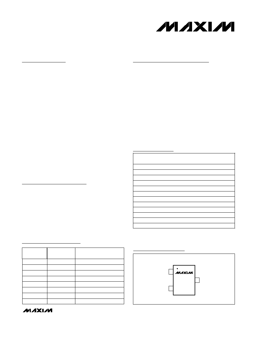
OUT
1
3
GND
IN
MAX6061
MAX6068
SOT23-3
TOP VIEW
2
19-1659; Rev 1; 4/01
Ordering Information
Pin Configuration
Selector Guide
Note: There is a minimum order increment of 2500 pieces for
SOT23 packages.
Typical Operating Circuit appears at end of data sheet.
PART
OUTPUT
VOLTAGE (V)
INPUT VOLTAGE (V)
MAX6061
1.248
2.5 to 12.6
MAX6062
2.048
2.5 to 12.6
MAX6066
2.500
(V
OUT
+ 200mV) to 12.6
MAX6063
3.000
(V
OUT
+ 200mV) to 12.6
MAX6064
4.096
(V
OUT
+ 200mV) to 12.6
MAX6067
4.500
(V
OUT
+ 200mV) to 12.6
MAX6065
5.000
(V
OUT
+ 200mV) to 12.6
MAX6068
1.800
2.5 to 12.6
PART
TEMP. RANGE
PIN-
PACKAGE
TOP
MARK
MAX6061AEUR-T -40°C to +85°C
3 SOT23-3
FZFP
MAX6061BEUR-T
-40°C to +85°C
3 SOT23-3
FZFQ
MAX6062AEUR-T -40°C to +85°C
3 SOT23-3
FZFY
MAX6062BEUR-T
-40°C to +85°C
3 SOT23-3
FZFZ
MAX6063AEUR-T -40°C to +85°C
3 SOT23-3
FZFV
MAX6063BEUR-T
-40°C to +85°C
3 SOT23-3
FZFW
MAX6064AEUR-T -40°C to +85°C
3 SOT23-3
FZGB
MAX6064BEUR-T
-40°C to +85°C
3 SOT23-3
FZGC
MAX6065AEUR-T -40°C to +85°C
3 SOT23-3
FZGE
MAX6065BEUR-T
-40°C to +85°C
3 SOT23-3
FZGF
MAX6066AEUR-T -40°C to +85°C
3 SOT23-3
FZFM
MAX6066BEUR-T
-40°C to +85°C
3 SOT23-3
FZFN
Ordering Information continued at end of data sheet.
For pricing, delivery, and ordering information, please contact Maxim/Dallas Direct! at
1-888-629-4642, or visit Maxim's website at www.maxim-ic.com.
MAX6061MAX6068
Precision, Micropower, Low-Dropout,
High-Output-Current, SOT23 Voltage References
2
_______________________________________________________________________________________
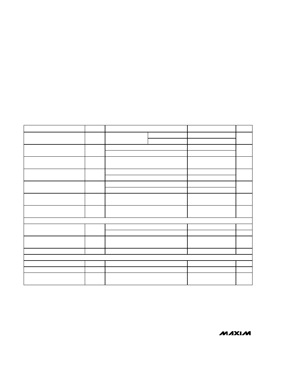
ABSOLUTE MAXIMUM RATINGS
ELECTRICAL CHARACTERISTICS--MAX6061, V
OUT
= 1.25V
(V
IN
= +5V, I
OUT
= 0, T
A
= T
MIN
to T
MAX
, unless otherwise noted. Typical values are at T
A
= +25°C.) (Note 1)
Stresses beyond those listed under "Absolute Maximum Ratings" may cause permanent damage to the device. These are stress ratings only, and functional
operation of the device at these or any other conditions beyond those indicated in the operational sections of the specifications is not implied. Exposure to
absolute maximum rating conditions for extended periods may affect device reliability.
(Voltages Referenced to GND)
IN .........................................................................-0.3V to +13.5V
OUT .............................................................-0.3V to (V
IN
+ 0.3V)
Output Short-Circuit Duration to GND or IN (V
IN
< 6V) ...Continuous
Output Short-Circuit Duration to GND or IN (V
IN
6V)................60s
Continuous Power Dissipation (T
A
= +70°C)
3-Pin SOT23 (derate 4.0mW/°C above +70°C)............320mW
Operating Temperature Range ...........................-40°C to +85°C
Storage Temperature Range .............................-65°C to +150°C
Lead Temperature (soldering, 10s) .................................+300°C
PARAMETER
SYMBOL
CONDITIONS
MIN
TYP
MAX
UNITS
MAX6061A (0.32%)
1.244
1.248
1.252
Output Voltage
V
OUT
T
A
= +25°C
MAX6061B (0.48%)
1.242
1.248
1.254
V
MAX6061A
6
20
Output Voltage Temperature
Coefficient (Note 2)
TCV
OUT
MAX6061B
6
30
ppm/°C
Line Regulation
V
OUT
/
V
IN
2.5V
V
IN
12.6V
10
90
µV/V
Sourcing: 0
I
OUT
5mA
0.5
0.9
Load Regulation
V
OUT
/
I
OUT
Sinking: -2mA
I
OUT
0
1.3
3.0
mV/mA
Short to GND
25
OUT Short-Circuit Current
I
SC
Short to IN
25
mA
Long-Term Stability
V
OUT
/
time
1000hr at +25°C
62
ppm/
1000hr
Output Voltage Hysteresis (Note 3)
V
OUT
/
cycle
130
ppm
DYNAMIC CHARACTERISTICS
f = 0.1Hz to 10Hz
13
µVp-p
Noise Voltage
e
OUT
f = 10Hz to 10kHz
15
µV
RMS
Ripple Rejection
V
OUT
/
V
IN
V
IN
= 5V ± 100mV, f = 120Hz
86
dB
Turn-On Settling Time
t
R
To V
OUT
= 0.1% of final value, C
OUT
= 50pF
50
µs
INPUT CHARACTERISTICS
Supply Voltage Range
V
IN
Guaranteed by line regulation test
2.5
12.6
V
Quiescent Supply Current
I
IN
90
125
µA
Change in Supply Current
I
IN
/
V
IN
2.5V
V
IN
12.6V
3.4
8.0
µA/V
MAX6061MAX6068
Precision, Micropower, Low-Dropout,
High-Output-Current, SOT23 Voltage References
_______________________________________________________________________________________
3
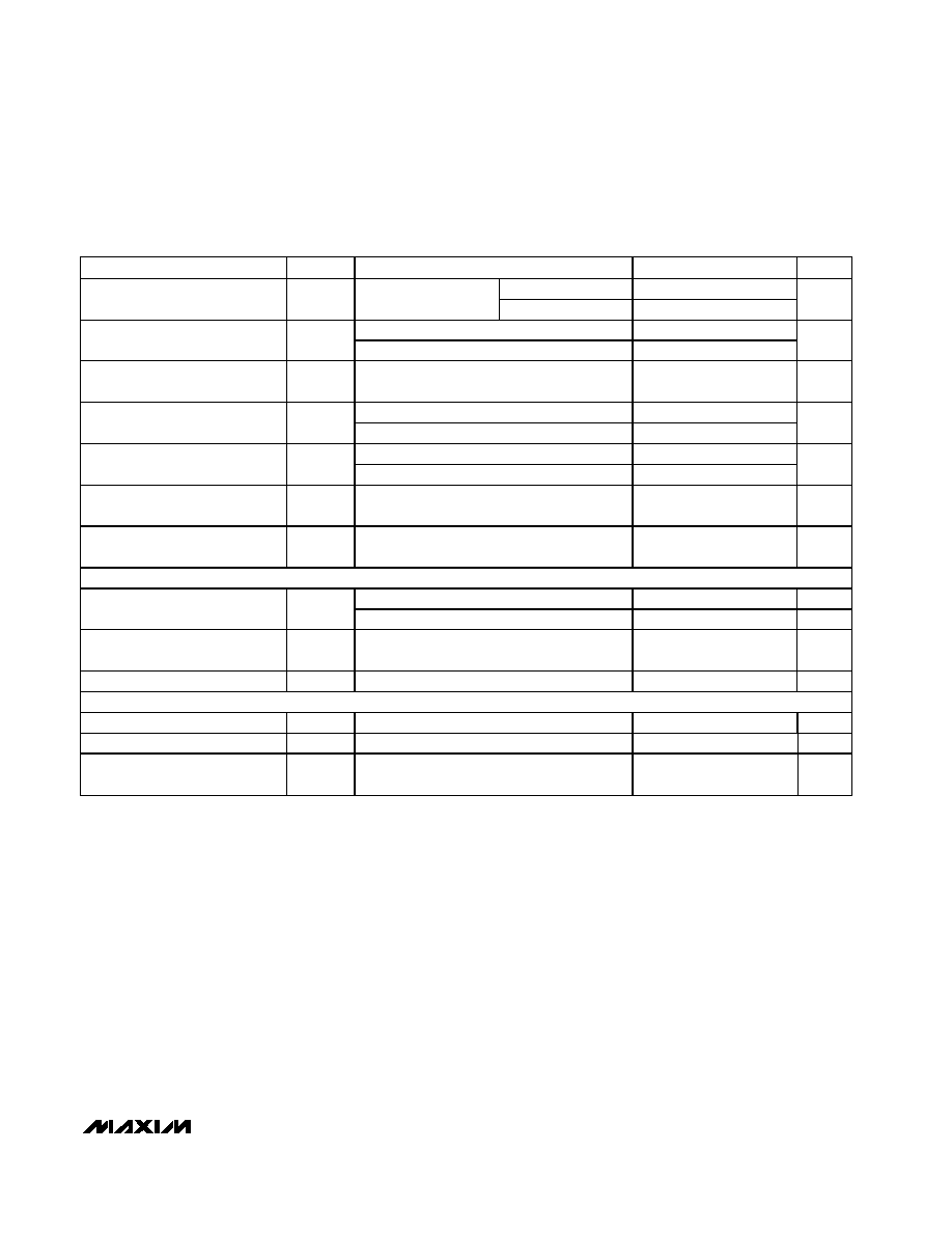
ELECTRICAL CHARACTERISTICS--MAX6068, V
OUT
= 1.80V
(V
IN
= +5V, T
A
= T
MIN
to T
MAX
, unless otherwise noted. Typical values are at T
A
= +25°C.) (Note 1)
PARAMETER
SYMBOL
CONDITIONS
MIN
TYP
MAX
UNITS
MAX6068A (0.17%)
1.797
1.800
1.803
Output Voltage
V
OUT
T
A
= +25
°C
MAX6068B (0.39%)
1.793
1.800
1.807
V
MAX6068A
6
20
Output Voltage Temperature
Coefficient (Note 2)
TCV
OUT
MAX6068B
6
30
ppm/
°C
Line Regulation
V
OUT
/
V
IN
2.5V
V
IN
12.6V
33
200
µV/V
Sourcing: 0
I
OUT
5mA
0.5
0.9
Load Regulation
V
OUT
/
I
OUT
Sinking: -2mA
I
OUT
0
1.5
4
mV/mA
Short to GND
25
OUT Short-Circuit Current
I
SC
Short to IN
25
mA
Long-Term Stability
V
OUT
/
time
1000hr at +25
°C
62
ppm/
1000hr
Output Voltage Hysteresis (Note 3)
V
OUT
/
cycle
130
ppm
DYNAMIC CHARACTERISTICS
f = 0.1Hz to 10Hz
22
µVp-p
Noise Voltage
e
OUT
f = 10Hz to 10kHz
25
µV
RMS
Ripple Rejection
V
OUT
/
V
IN
V
IN
= 5V
±100mV, f = 120Hz
86
dB
Turn-On Settling Time
t
R
To V
OUT
= 0.1% of final value, C
OUT
= 50pF
115
µs
INPUT CHARACTERISTICS
Supply Voltage Range
V
IN
Guaranteed by line regulation test
2.5
12.6
V
Quiescent Supply Current
I
IN
90
125
µA
Change in Supply Current
I
IN
/
V
IN
2.5V
V
IN
12.6V
3.3
8.0
µA/V
MAX6061MAX6068
Precision, Micropower, Low-Dropout,
High-Output-Current, SOT23 Voltage References
4
_______________________________________________________________________________________
ELECTRICAL CHARACTERISTICS--MAX6062, V
OUT
= 2.048V
(V
IN
= +5V, I
OUT
= 0, T
A
= T
MIN
to T
MAX
, unless otherwise noted. Typical values are at T
A
= +25°C.) (Note 1)
MAX6062B (0.39%)
MAX6062A (0.24%)
Output Voltage
V
OUT
2.043
2.048
2.053
PARAMETER
SYMBOL
MIN
TYP
MAX
UNITS
OUT Short-Circuit Current
I
SC
25
mA
1.5
4
Load Regulation
V
OUT
/
I
OUT
0.5
0.9
mV/mA
Line Regulation
V
OUT
/
V
IN
33
200
µV/V
25
Long-Term Stability
V
OUT
/
time
62
ppm/
1000hr
Output Voltage Hysteresis
(Note 3)
V
OUT
/
cycle
130
ppm
Output Voltage Temperature
Coefficient (Note 2)
2.040
2.048
2.056
TCV
OUT
6
20
ppm/°C
6
30
Noise Voltage
e
OUT
22
µVp-p
25
µV
RMS
Ripple Rejection
V
OUT
/
V
IN
86
dB
Turn-On Settling Time
t
R
115
µs
Supply Voltage Range
V
IN
2.5
12.6
V
Quiescent Supply Current
I
IN
90
125
µA
Change in Supply Current
I
IN
/V
IN
3.3
8.0
µA/V
CONDITIONS
f = 0.1Hz to 10Hz
Short to GND
f = 10Hz to 10kHz
Sinking: -2mA
I
OUT
0
Sourcing: 0
I
OUT
5mA
2.5V
V
IN
12.6V
Short to IN
1000hr at +25°C
V
IN
= 5V ±100mV, f = 120Hz
To V
OUT
= 0.1% of final value, C
OUT
= 50pF
Guaranteed by line-regulation test
T
A
= +25°C
MAX6062A
2.5V
V
IN
12.6V
MAX6062B
V
DYNAMIC CHARACTERISTICS
INPUT CHARACTERISTICS
MAX6061MAX6068
Precision, Micropower, Low-Dropout,
High-Output-Current, SOT23 Voltage References
_______________________________________________________________________________________
5
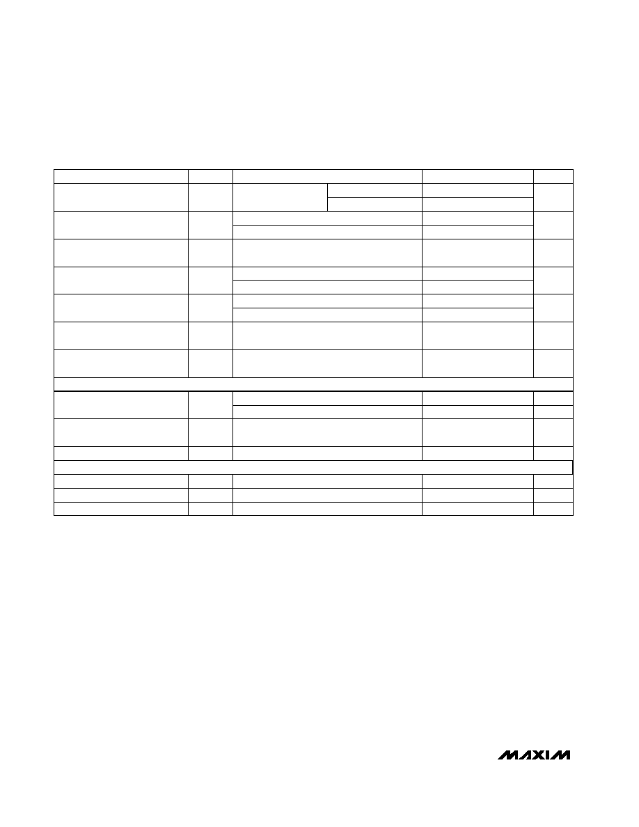
ELECTRICAL CHARACTERISTICS--MAX6066, V
OUT
= 2.500V
(V
IN
= +5V, I
OUT
= 0, T
A
= T
MIN
to T
MAX
, unless otherwise noted. Typical values are at T
A
= +25°C.) (Note 1)
MAX6066B (0.4%)
MAX6066A (0.2%)
T
A
= +25°C
V
2.495
2.500
2.505
V
OUT
Output Voltage
MAX6066B
(V
OUT
+ 0.2V)
V
IN
12.6V
MAX6066A
Guaranteed by line-regulation test
To V
OUT
= 0.1% of final value, C
OUT
= 50pF
V
IN
= 5V ±100mV, f = 120Hz
1000hr at +25°C
Short to IN
(V
OUT
+ 0.2V)
V
IN
12.6V
Sourcing: 0
I
OUT
5mA
Sinking: -2mA
I
OUT
0
f = 10Hz to 10kHz
Short to GND
f = 0.1Hz to 10Hz
CONDITIONS
µA/V
3.3
8.0
I
IN
/V
IN
Change in Supply Current
µA
90
125
I
IN
Quiescent Supply Current
V
V
OUT
+ 0.2
12.6
V
IN
Supply Voltage Range
µs
115
t
R
Turn-On Settling Time
dB
86
V
OUT
/
V
IN
Ripple Rejection
µV
RMS
30
µVp-p
27
e
OUT
Noise Voltage
6
30
ppm/°C
6
20
TCV
OUT
2.490
2.500
2.510
Output Voltage Temperature
Coefficient (Note 2)
ppm
130
V
OUT
/
cycle
Output Voltage Hysteresis
(Note 3)
ppm/
1000hr
62
V
OUT
/
time
Long-Term Stability
25
µV/V
60
300
V
OUT
/
V
IN
Line Regulation
mV/mA
0.5
0.9
V
OUT
/
I
OUT
Load Regulation
1.6
5
mA
25
I
SC
OUT Short-Circuit Current
UNITS
MIN
TYP
MAX
SYMBOL
PARAMETER
I
OUT
= 1mA
mV
50
200
V
IN
-
V
OUT
Dropout Voltage (Note 4)
DYNAMIC CHARACTERISTICS
INPUT CHARACTERISTICS