
________________General Description
The MAX6315 low-power CMOS microprocessor (µP)
supervisory circuit is designed to monitor power sup-
plies in µP and digital systems. It provides excellent cir-
cuit reliability and low cost by eliminating external
components and adjustments. The MAX6315 also pro-
vides a debounced manual reset input.
This device performs a single function: it asserts a reset
signal whenever the V
CC
supply voltage falls below a
preset threshold or whenever manual reset is asserted.
Reset remains asserted for an internally programmed
interval (reset timeout period) after V
CC
has risen above
the reset threshold or manual reset is deasserted. The
MAX6315's open-drain RESET output can be pulled up
to a voltage higher than V
CC
.
The MAX6315 comes with factory-trimmed reset thresh-
old voltages in 100mV increments from 2.5V to 5V.
Preset timeout periods of 1ms, 20ms, 140ms, and
1120ms (minimum) are also available. The device
comes in a SOT143 package.
For microcontrollers (µCs) and µPs with bidirectional
reset pins, see the MAX6314 data sheet.
________________________Applications
Computers
Controllers
Intelligent Instruments
Critical µP and µC Power Monitoring
Portable/Battery-Powered Equipment
____________________________Features
o
Small SOT143 Package
o
Open-Drain
RESET
Output Can Exceed V
CC
o
Precision, Factory-Set V
CC
Reset Thresholds:
100mV Increments from 2.5V to 5V
o
±1.8% Reset Threshold Accuracy at T
A
= +25∞C
o
±2.5% Reset Threshold Accuracy Over Temp.
o
Four Reset Timeout Periods Available:
1ms, 20ms, 140ms, or 1120ms (minimum)
o
Immune to Short V
CC
Transients
o
5µA Supply Current
o
Pin-Compatible with MAX811
MAX6315
Open-Drain SOT µP Reset Circuit
________________________________________________________________
Maxim Integrated Products
1
1
2
4
3
V
CC
MR
RESET
GND
MAX6315
SOT143
TOP VIEW
__________________Pin Configuration
MAX6315
V
CC
V
CC
GND
RESET
µP
RESET
MR
LASER-
TRIMMED
RESISTORS
RESET
CIRCUITRY
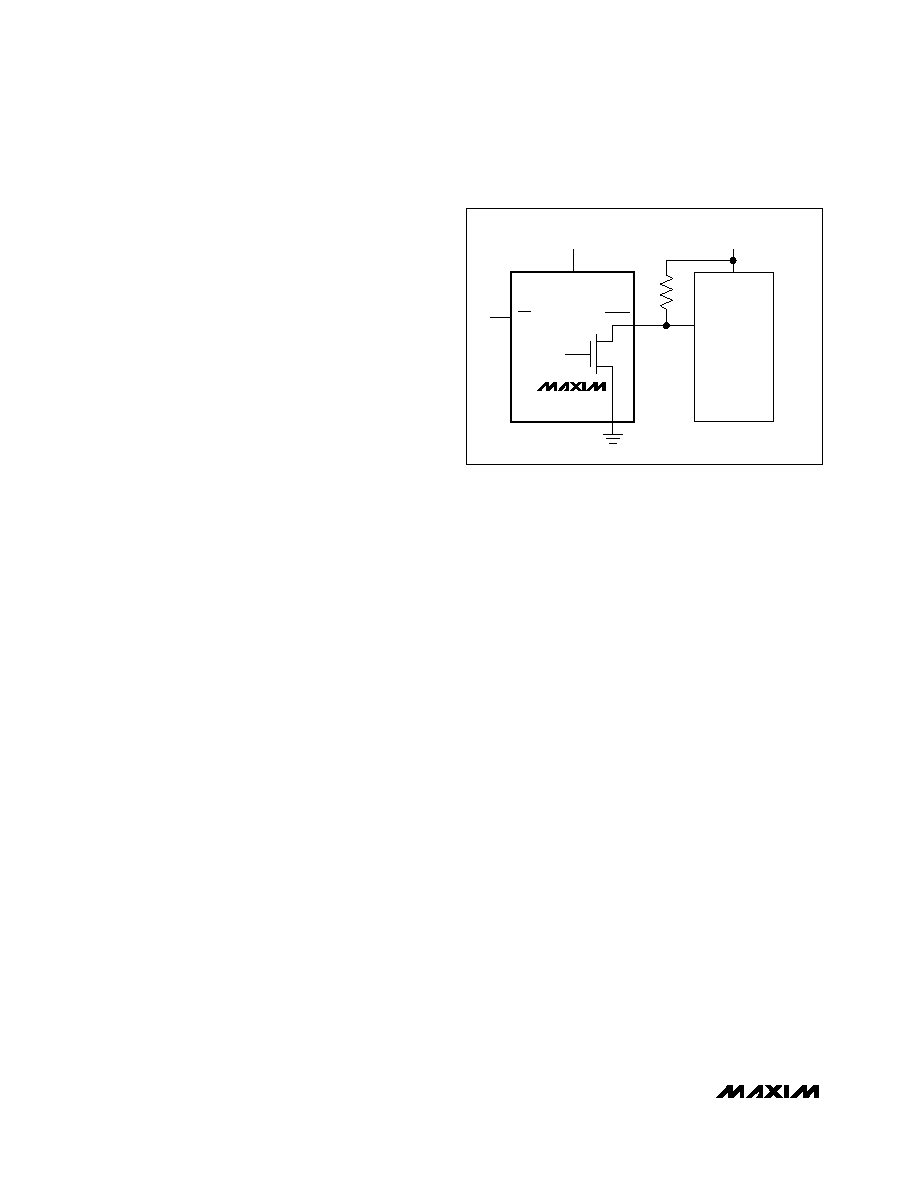
__________Typical Operating Circuit
19-2000; Rev 1; 1/99
Ordering and Marking Information appear at end of
data sheet.
For free samples & the latest literature: http://www.maxim-ic.com, or phone 1-800-998-8800.
For small orders, phone 1-800-835-8769.
MAX6315
Open-Drain SOT µP Reset Circuit
2
_______________________________________________________________________________________
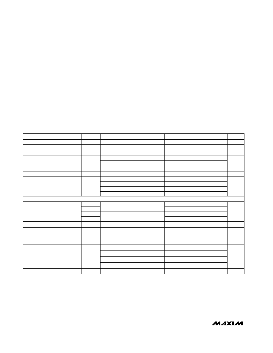
ABSOLUTE MAXIMUM RATINGS
ELECTRICAL CHARACTERISTICS
(V
CC
= +2.5V to +5.5V, T
A
= -40∞C to +85∞C, unless otherwise noted. Typical values are at T
A
= +25∞C.)
Stresses beyond those listed under "Absolute Maximum Ratings" may cause permanent damage to the device. These are stress ratings only, and functional
operation of the device at these or any other conditions beyond those indicated in the operational sections of the specifications is not implied. Exposure to
absolute maximum rating conditions for extended periods may affect device reliability.
Note 1:
The MAX6315 monitors V
CC
through an internal factory-trimmed voltage divider that programs the nominal reset threshold.
Factory-trimmed reset thresholds are available in 100mV increments from 2.5V to 5V (see
Ordering and Marking
Information).
V
CC
........................................................................-0.3V to +6.0V
RESET....................................................................-0.3V to +6.0V
All Other Pins..............................................-0.3V to (V
CC
+ 0.3V)
Input Current (V
CC
) .............................................................20mA
Output Current (RESET)......................................................20mA
Rate of Rise (V
CC
) ...........................................................100V/µs
Continuous Power Dissipation (T
A
= +70∞C)
SOT143 (derate 4mW/∞C above +70∞C) ........................320mW
Operating Temperature Range ...........................-40∞C to +85∞C
Storage Temperature Range .............................-65∞C to +160∞C
Lead Temperature (soldering, 10sec) .............................+300∞C
MAX6315US_ _D3-T
MAX6315US_ _D2-T
MAX6315US_ _D4-T
T
A
= +25∞C
V
CC
> 1.2V, I
SINK
= 0.5mA
V
CC
= 5.5V, no load
4
10
T
A
= -40∞C to +85∞C
V
TH
- 2.5%
V
TH
+ 2.5%
1120
1570
2240
140
200
280
20
28
40
V
CC
> V
TH
, RESET deasserted
V
TH
> 4.0V
V
CC
= falling at 1mV/µs
MAX6315US_ _D1-T
V
CC
> 4.25V, I
SINK
= 3.2mA
CONDITIONS
V
CC
> 2.5V, I
SINK
= 1.2mA
V
CC
> 1.0V, I
SINK
= 80µA
0.3 x V
CC
2.4
0.7 x V
CC
0.3
0.3
V
µA
1
RESET Output Leakage Current
V
0.4
V
OL
RESET Output Voltage
k
32
63
100
MR Pull-Up Resistance
V
TH
- 1.8%
V
TH
V
TH
+ 1.8%
V
TH
Reset Threshold (Note 1)
µA
5
12
I
CC
V
1.0
5.5
V
CC
Operating Voltage Range
V
CC
Supply Current
ns
500
MR to Reset Delay
ns
100
MR Glitch Rejection
µs
1
MR Minimum Input Pulse
V
0.8
V
IL
MR Input Threshold
ppm/∞C
60
V
TH
/∞C
Reset Threshold Tempco
µs
35
V
CC
to Reset Delay
ms
1
1.4
2
t
RP
Reset Timeout Period
UNITS
MIN
TYP
MAX
SYMBOL
PARAMETER
V
IL
V
IH
V
IH
V
CC
= 3.6V, no load
T
A
= -40∞C to +85∞C
V
TH
< 4.0V
MANUAL RESET INPUT
MAX6315
Open-Drain SOT µP Reset Circuit
_______________________________________________________________________________________
3
6
0
-50
-30
30
90
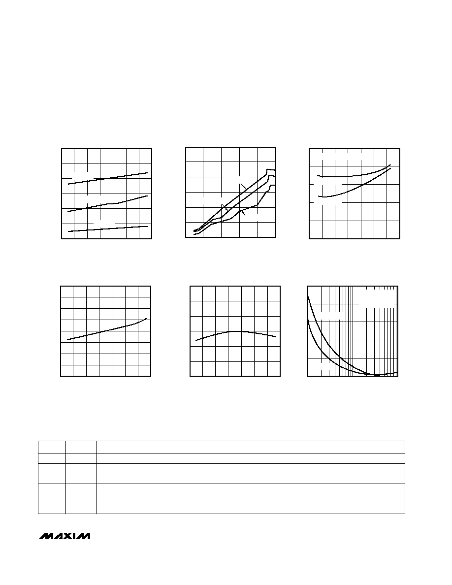
SUPPLY CURRENT vs. TEMPERATURE
2
1
5
MAX6315-01
TEMPERATURE (∞C)
SUPPLY CURRENT (
µ
A)
-10
10
50
3
4
70
V
CC
= 5V
V
CC
= 3V
V
CC
= 1V
6
0
0
1
3
5
SUPPLY CURRENT
vs. SUPPLY VOLTAGE
2
1
5
MAX6315-02
SUPPLY VOLTAGE (V)
SUPPLY CURRENT (
µ
A)
2
3
4
4
T
A
= -40∞C
T
A
= +25∞C
T
A
= +85∞C
50
0
-50
-30
10
90
POWER-DOWN RESET DELAY
vs. TEMPERATURE
10
40
MAX6315-03
TEMPERATURE (∞C)
POWER-DOWN RESET DELAY (
µ
s)
-10
20
30
30
50
70
V
CC
FALLING AT 1mV/
µ
s
V
TH
= 4.63V
V
TH
= 3.00V
1.04
0.96
-50
-30
10
90
NORMALIZED RESET TIMEOUT PERIOD
vs. TEMPERATURE (V
CC
RISING)
0.97
0.98
1.02
1.00
1.03
MAX6315-04
TEMPERATURE (∞C)
NORMALIZED RESET TIMEOUT PERIOD
-10
0.99
1.01
30
50
70
1.006
0.994
-50
-30
10
90
NORMALIZED RESET THRESHOLD
vs. TEMPERATURE (V
CC
FALLING)
0.996
0.998
1.004
1.000
MAX6315-05
TEMPERATURE (∞C)
NORMALIZED RESET THRESHOLD
-10
1.002
30
50
70
100
0
10
100
1000
MAXIMUM TRANSIENT DURATION
vs. RESET COMPARATOR OVERDRIVE
20
MAX6315-06
RESET COMP. OVERDRIVE, V
TH
- V
CC
(mV)
MAXIMUM TRANSIENT DURATION (
µ
s)
40
60
80
T
A
= +25∞C
RESET OCCURS
ABOVE CURVE
V
TH
= 4.63V
V
T
= 3.00V
__________________________________________Typical Operating Characteristics
(T
A
= +25∞C, unless otherwise noted.)
______________________________________________________________Pin Description
NAME
FUNCTION
1
GND
Ground
2
RESET
Active-Low Open-Drain Output. Connect to an external pull-up resistor. Can be pulled up to a voltage
higher than V
CC
, but less than 6V.
PIN
3
MR
Manual Reset Input. A logic low on MR asserts reset. Reset remains asserted as long as MR is low, and
for the reset timeout period (t
RP
) after the reset conditions are terminated. Connect to V
CC
if not used.
4
V
CC
Supply Voltage and Reset Threshold Monitor Input
_______________Detailed Description
Reset Output
A microprocessor's (µP's) reset input starts the µP in a
known state. The MAX6315 asserts reset to prevent
code-execution errors during power-up, power-down,
or brownout conditions. RESET is guaranteed to be a
logic low for V
CC
> 1V (see
Electrical Characteristics).
Once V
CC
exceeds the reset threshold, the internal
timer keeps reset asserted for the reset timeout period
(t
RP
); after this interval RESET goes high. If a brownout
condition occurs (monitored voltage dips below its pro-
grammed reset threshold), RESET goes low. Any time
V
CC
dips below the reset threshold, the internal timer
resets to zero and RESET goes low. The internal timer
starts when V
CC
returns above the reset threshold, and
RESET remains low for the reset timeout period.
The MAX6315's RESET output structure is a simple
open-drain N-channel MOSFET switch. Connect a pull-
up resistor to any supply in the 0V to +6V range. Select
a resistor value large enough to register a logic low
when RESET is asserted (see
Electrical Characteristics),
and small enough to register a logic high while supply-
ing all input current and leakage paths connected to the
RESET line. A 10k
pull-up is sufficient in most applica-
tions.
Often, the pull-up connected to the MAX6315's RESET
output will connect to the supply voltage monitored at
the IC's V
CC
pin. However, some systems may use the
open-drain output to level-shift from the monitored sup-
ply to reset circuitry powered by some other supply
(Figure 1). This is one useful feature of an open-drain
output. Keep in mind that as the MAX6315's V
CC
decreases below 1V, so does the IC's ability to sink
current at RESET. Finally, with any pull-up, RESET will
be pulled high as V
CC
decays toward 0V. The voltage
where this occurs depends on the pull-up resistor value
and the voltage to which it connects (see
Electrical
Characteristics).
Manual-Reset Input
Many µP-based products require manual-reset capabil-
ity, allowing the operator, a test technician, or external
logic circuitry to initiate a reset. A logic low on MR
asserts reset. Reset remains asserted while MR is low,
and for the reset active timeout period after MR returns
high.
MR has an internal 63k
pull-up resistor, so it can be
left open if not used. Connect a normally open momen-
tary switch from MR to GND to create a manual reset
function; external debounce circuitry is not required.
If MR is driven from long cables or if the device is used
in a noisy environment, connecting a 0.1µF capacitor
from MR to ground provides additional noise immunity.
__________Applications Information
Negative-Going V
CC
Transients
In addition to issuing a reset to the µP during power-up,
power-down, and brownout conditions, these devices
are relatively immune to short-duration negative-going
transients (glitches). The
Typical Operating Character-
istics show the Maximum Transient Duration vs. Reset
Threshold Overdrive, for which reset pulses are not
generated. The graph was produced using negative-
going pulses, starting at V
RST
max and ending below
the programmed reset threshold by the magnitude indi-
cated (reset threshold overdrive). The graph shows the
maximum pulse width that a negative-going V
CC
tran-
sient may typically have without causing a reset pulse
to be issued. As the transient amplitude increases (i.e.,
goes farther below the reset threshold), the maximum
allowable pulse width decreases. A 0.1µF bypass
capacitor mounted close to V
CC
provides additional
transient immunity.
MAX6315
Open-Drain SOT µP Reset Circuit
4
_______________________________________________________________________________________
Figure 1. MAX6315 Open-Drain RESET Output Allows Use
with Multiple Supplies
MAX6315
V
CC
GND
RESET
MR
5V SYSTEM
+5.0V
+3.3V
10k
MAX6315
Open-Drain SOT µP Reset Circuit
_______________________________________________________________________________________
5
________________________________________________________Ordering Information
PART
NOMINAL
V
TH
(V)
MIN t
RP
(ms)
SOT TOP
MARK
MAX6315US50D1-T
5.00
1
FX_ _
MAX6315US45D1-T
4.50
1
GC_ _
MAX6315US44D1-T
4.39
1
GD_ _
MAX6315US43D1-T
4.30
1
GE_ _
MAX6315US42D1-T
4.20
1
GF_ _
MAX6315US41D1-T
4.10
1
GG_ _
MAX6315US40D1-T
4.00
1
GH_ _
MAX6315US39D1-T
3.90
1
GI_ _
MAX6315US38D1-T
3.80
1
GJ_ _
MAX6315US37D1-T
3.70
1
GK_ _
MAX6315US36D1-T
3.60
1
GL_ _
MAX6315US35D1-T
3.50
1
GM_ _
MAX6315US34D1-T
3.40
1
GN_ _
MAX6315US33D1-T
3.30
1
GO_ _
MAX6315US32D1-T
3.20
1
GP_ _
MAX6315US31D1-T
3.08
1
GQ_ _
MAX6315US30D1-T
3.00
1
GR_ _
MAX6315US29D1-T
2.93
1
GS_ _
The MAX6315 is available in a SOT143 package, -40∞C to +85∞C temperature range.
The first two letters in the package top mark identify the part, while the remaining two letters are the lot tracking code.
Sample stocks generally held on the bolded products; also, the bolded products have 2,500 piece minimum-order quantities.
Non-bolded products have 10,000 piece minimum-order quantities. Contact factory for details.
Note:
All devices available in tape-and-reel only. Contact factory for availability.
PART
MAX6315US37D2-T
3.70
20
HK_ _
MAX6315US36D2-T
3.60
NOMINAL
V
TH
(V)
MIN t
RP
(ms)
20
HL_ _
SOT TOP
MARK
MAX6315US50D2-T
5.00
20
GX_ _
MAX6315US49D2-T
4.90
20
GY_ _
MAX6315US48D2-T
4.80
20
GZ_ _
MAX6315US47D2-T
4.70
20
HA_ _
MAX6315US46D2-T
4.63
20
HB_ _
MAX6315US45D2-T
4.50
20
HC_ _
MAX6315US44D2-T
4.39
20
HD_ _
MAX6315US43D2-T
4.30
20
HE_ _
MAX6315US42D2-T
4.20
20
HF_ _
MAX6315US41D2-T
4.10
20
HG_ _
MAX6315US40D2-T
4.00
20
HH_ _
MAX6315US39D2-T
3.90
20
HI_ _
MAX6315US38D2-T
3.80
20
HJ_ _
MAX6315US34D2-T
3.40
20
HN_ _
MAX6315US33D2-T
3.30
20
HO_ _
MAX6315US35D2-T
3.50
20
HM_ _
MAX6315US47D1-T
4.70
1
GA_ _
MAX6315US48D1-T
4.80
1
FZ_ _
MAX6315US46D1-T
4.63
1
GB_ _
MAX6315US49D1-T
4.90
1
FY_ _
MAX6315US26D1-T
2.63
1
GV_ _
MAX6315US27D1-T
2.70
1
GU_ _
MAX6315US28D1-T
2.80
1
GT_ _
MAX6315US25D1-T
2.50
1
GW_ _
MAX6315US29D2-T
2.93
20
HS_ _
MAX6315US28D2-T
2.80
20
HT_ _
MAX6315US26D2-T
2.63
20
HV_ _
MAX6315US25D2-T
2.50
20
HW_ _
MAX6315US27D2-T
2.70
20
HU_ _
MAX6315US32D2-T
4.20
20
HP_ _
MAX6315US31D2-T
3.08
20
HQ_ _
MAX6315US30D2-T
3.00
20
HR_ _