MAX6316 DS
___________________________________________________________________Selector Guide
________________General Description
The MAX6316MAX6322 family of microprocessor (µP)
supervisory circuits monitors power supplies and
microprocessor activity in digital systems. It offers sev-
eral combinations of push/pull, open-drain, and bidirec-
tional (such as Motorola 68HC11) reset outputs, along
with watchdog and manual reset features. The Selector
Guide below lists the specific functions available from
each device. These devices are specifically designed
to ignore fast negative transients on V
CC
. Resets are
guaranteed valid for V
CC
down to 1V.
These devices are available in 26 factory-trimmed reset
threshold voltages (from 2.5V to 5V, in 100mV incre-
ments), featuring four minimum power-on reset timeout
periods (from 1ms to 1.12s), and four watchdog timeout
periods (from 6.3ms to 25.6s). Thirteen standard ver-
sions are available with an order increment requirement
of 2500 pieces (see Standard Versions table); contact
the factory for availability of other versions, which have
an order increment requirement of 10,000 pieces.
The MAX6316MAX6322 are offered in a miniature
5-pin SOT23 package.
________________________Applications
Portable Computers
Computers
Controllers
Intelligent Instruments
Portable/Battery-Powered Equipment
Embedded Control Systems
____________________________Features
o Small 5-Pin SOT23 Package
o Available in 26 Reset Threshold Voltages
2.5V to 5V, in 100mV Increments
o Four Reset Timeout Periods
1ms, 20ms, 140ms, or 1.12s (min)
o Four Watchdog Timeout Periods
6.3ms, 102ms, 1.6s, or 25.6s (typ)
o Four Reset Output Stages
Active-High, Push/Pull
Active-Low, Push/Pull
Active-Low, Open-Drain
Active-Low, Bidirectional
o Guaranteed Reset Valid to V
CC
= 1V
o Immune to Short Negative V
CC
Transients
o Low Cost
o No External Components
MAX6316MAX6322
5-Pin µP Supervisory Circuits with
Watchdog and Manual Reset
________________________________________________________________ Maxim Integrated Products
1
19-0496; Rev 5; 9/02
PART
MAX6316LUK____-T
MAX6316MUK____-T
-40°C to +85°C
-40°C to +85°C
TEMP RANGE
PIN-PACKAGE
5 SOT23-5
5 SOT23-5
_______________Ordering Information
Ordering Information continued at end of data sheet.
MAX6317HUK____-T
-40°C to +85°C
5 SOT23-5
MAX6318HUK____-T
-40°C to +85°C
5 SOT23-5
ACTIVE-LOW
OPEN-DRAIN
MAX6316L
MAX6316M
MAX6317H
MAX6321HP
MAX6318LH
--
MAX6318MH
--
MAX6319LH
--
MAX6319MH
--
MAX6320P
ACTIVE-LOW
PUSH/PULL
--
--
--
--
--
ACTIVE-HIGH
PUSH/PULL
--
--
--
ACTIVE-LOW
BIDIRECTIONAL
--
--
--
--
--
PART
WATCHDOG
INPUT
MANUAL
RESET
INPUT
--
--
--
--
MAX6322HP
--
--
--
--
--
--
--
RESET OUTPUTS*
--
--
* The MAX6318/MAX6319/MAX6321/MAX6322 feature two types of reset output on each device.
MAX6318MHUK____-T
-40°C to +85°C
5 SOT23-5
Typical Operating Circuit and Pin Configurations appear at
end of data sheet.
For pricing, delivery, and ordering information, please contact Maxim/Dallas Direct! at
1-888-629-4642, or visit Maxim's website at www.maxim-ic.com.
ELECTRICAL CHARACTERISTICS
(V
CC
= 2.5V to 5.5V, T
A
= -40°C to +85°C, unless otherwise noted. Typical values are at T
A
= +25°C.) (Note 1)
MAX6316MAX6322
5-Pin µP Supervisory Circuits with
Watchdog and Manual Reset
2
_______________________________________________________________________________________
ABSOLUTE MAXIMUM RATINGS
Stresses beyond those listed under "Absolute Maximum Ratings" may cause permanent damage to the device. These are stress ratings only, and functional
operation of the device at these or any other conditions beyond those indicated in the operational sections of the specifications is not implied. Exposure to
absolute maximum rating conditions for extended periods may affect device reliability.
Voltage (with respect to GND)
V
CC
......................................................................-0.3V to +6V
RESET (MAX6320/MAX6321/MAX6322 only)...... -0.3V to +6V
All Other Pins.........................................-0.3V to (V
CC
+ 0.3V)
Input/Output Current, All Pins .............................................20mA
Continuous Power Dissipation (T
A
= +70°C)
SOT23-5 (derate 7.1mW/°C above +70°C)...............571mW
Operating Temperature Range............................-40°C to +85°C
Junction Temperature ......................................................+150°C
Storage Temperature Range..............................-65°C to +160°C
Lead Temperature (soldering, 10s) .................................+300°C
Note 1: Over-temperature limits are guaranteed by design, not production tested.
Note 2: A factory-trimmed voltage divider programs the nominal reset threshold (V
TH
). Factory-trimmed reset thresholds are
available in 100mV increments from 2.5V to 5V (see Table 1 at end of data sheet).
Note 3: Guaranteed by design.
PARAMETER
SYMBOL
CONDITIONS
MIN
TYP
MAX
UNITS
Operating Voltage Range
V
CC
T
A
= -40°C to +85°C
1.0
5.5
V
V
CC
= 5.5V
10
20
MAX6316/MAX6317/MAX
6318/MAX6320/MAX6321
V
CC
= 3.6V
5
12
V
CC
= 5.5V
3
12
Supply Current
I
CC
MAX6319/MAX6322:
MR unconnected
V
CC
= 3.6V
3
8
µA
Reset Threshold
Temperature Coefficient
V
TH
/°C
40
ppm/°C
T
A
= +25°C
V
TH
- 1.5%
V
TH
V
TH
+ 1.5%
Reset Threshold (Note 2)
V
RST
T
A
= -40°C to +85°C
V
TH
- 2.5%
V
TH
V
TH
+ 2.5%
V
Reset Threshold Hysteresis
3
mV
MAX63_ _ A_-T
1
1.4
2
MAX63_ _ B_-T
20
28
40
MAX63_ _ C_-T
140
200
280
Reset Active Timeout Period
t
RP
MAX63_ _ D_-T
1120
1600
2240
ms
V
CC
to RESET Delay
t
RD
V
CC
falling at 1mV/µs
40
µs
PUSH/PULL RESET OUTPUT (MAX6316L/MAX6317H/MAX6318_H/MAX6319_H/MAX6321HP/MAX6322HP)
V
CC
1.0V, I
SINK
= 50µA
0.3
V
CC
1.2V, I
SINK
= 100µA
0.3
V
CC
2.7V, I
SINK
= 1.2mA
0.3
V
OL
V
CC
4.5V, I
SINK
= 3.2mA
0.4
V
CC
2.7V, I
SOURCE
= 500µA
0.8 x V
CC
RESET Output Voltage
V
OH
V
CC
4.5V, I
SOURCE
= 800µA
V
CC
- 1.5
V
RES ET Ri se Ti m e ( M AX 6316L,
M AX 6318LH , M AX 6319LH )
t
R
Rise time is measured from 10% to 90%
of V
CC
; C
L
= 5pF, V
CC
= 3.3V (Note 3)
5
25
ns
V
CC
2.7V, I
SINK
= 1.2mA
0.3
V
OL
V
CC
4.5V, I
SINK
= 3.2mA
0.4
V
CC
1.8V, I
SOURCE
= 150µA
0.8 x V
CC
V
CC
2.7V, I
SOURCE
= 500µA
0.8 x V
CC
RESET Output Voltage
V
OH
V
CC
4.5V, I
SOURCE
= 800µA
V
CC
- 1.5
V
MAX6316MAX6322
5-Pin µP Supervisory Circuits with
Watchdog and Manual Reset
_______________________________________________________________________________________
3
Note 4: This is the minimum time RESET must be held low by an external pulldown source to set the active pullup flip-flop.
Note 5: Measured from RESET V
OL
to (0.8 x V
CC
), R
LOAD
=
.
Note 6: WDI is internally serviced within the watchdog period if WDI is left unconnected.
Note 7: The WDI input current is specified as the average input current when the WDI input is driven high or low. The WDI input is
designed for a three-stated-output device with a 10µA maximum leakage current and capable of driving a maximum capaci-
tive load of 200pF. The three-state device must be able to source and sink at least 200µA when active.
µA
1.0
I
LKG
Open-Drain Reset Output
Leakage Current
ns
400
t
S
Transition Flip-Flop Setup Time
333
ns
333
t
R
RESET Output Rise Time
(Note 5)
UNITS
MIN
TYP
MAX
SYMBOL
PARAMETER
(Note 4)
V
CC
= 5.0V, C
L
= 200pF
V
CC
= 3.0V, C
L
= 120pF
CONDITIONS
ELECTRICAL CHARACTERISTICS (continued)
(V
CC
= 2.5V to 5.5V, T
A
= -40°C to +85°C, unless otherwise noted. Typical values are at T
A
= +25°C.) (Note 1)
666
666
V
CC
= 5.0V, C
L
= 400pF
V
CC
= 3.0V, C
L
= 250pF
V
0.4
0.65
V
PTH
Active Pullup Enable Threshold
V
CC
= 5.0V
mA
20
RESET Active Pullup Current
V
CC
= 5.0V
k
4.2
4.7
5.2
RESET Pullup Resistance
V
0.3
V
OL
RESET Output Voltage
V
CC
1.0V, I
SINK
= 50µA
0.3
V
CC
1.2V, I
SINK
= 100µA
0.3
V
CC
2.7V, I
SINK
= 1.2mA
0.4
V
CC
4.5V, I
SINK
= 3.2mA
ms
4.3
6.3
9.3
t
WD
Watchdog Timeout Period
MAX63_ _ _ W-T
71
102
153
MAX63_ _ _ X-T
s
1.12
1.6
2.4
MAX63_ _ _ Y-T
17.9
25.6
38.4
MAX63_ _ _ Z-T
ns
50
t
WDI
WDI Pulse Width
V
IL
= 0.3 x V
CC
, V
IH
= 0.7 x V
CC
V
0.3 x V
CC
V
IL
WDI Input Threshold
(Note 6)
0.7 x V
CC
120
160
I
WDI
WDI Input Current
(Note 7)
WDI = V
CC
, time average
-20
-15
V
WDI
= 0, time average
V
IH
V
0.8
V
IL
MR Input Threshold
V
TH
> 4.0V
2.0
V
IH
0.3 x V
CC
V
IL
V
TH
< 4.0V
0.7 x V
CC
V
IH
µs
1
MR Input Pulse Width
ns
100
MR Glitch Rejection
k
35
52
75
MR Pullup Resistance
ns
230
MR to Reset Delay
V
CC
= 5V
µA
BIDIRECTIONAL RESET OUTPUT (MAX6316M/MAX6318MH/MAX6319MH)
OPEN-DRAIN RESET OUTPUT (MAX6320P/MAX6321HP/MAX6322HP)
WATCHDOG INPUT (MAX6316/MAX6317H/MAX6318_H/MAX6320P/MAX6321HP)
MANUAL RESET INPUT (MAX6316_/MAX6317H/MAX6319_H/MAX6320P/MAX6322HP)
MAX6316MAX6322
5-Pin µP Supervisory Circuits with
Watchdog and Manual Reset
4
_______________________________________________________________________________________
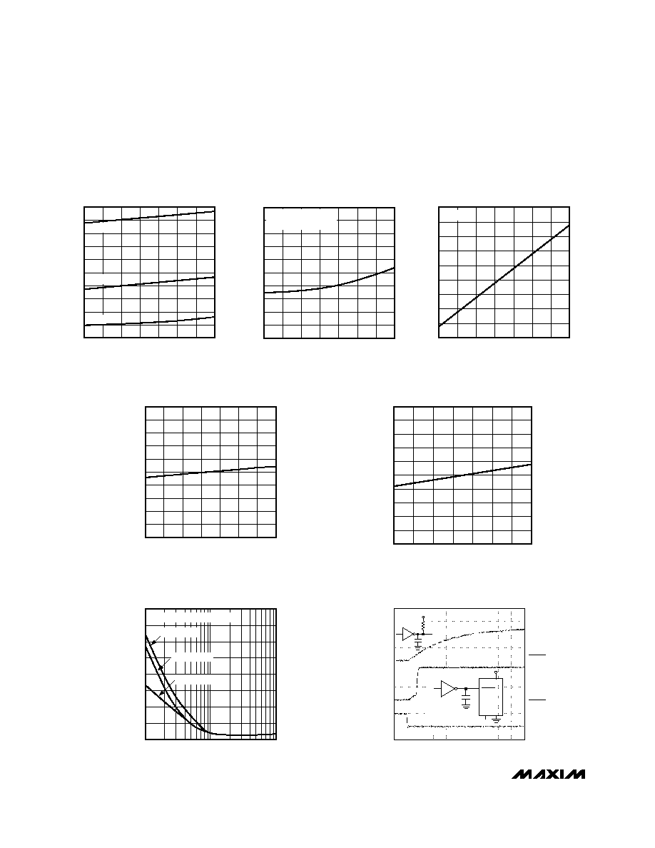
__________________________________________Typical Operating Characteristics
(T
A
= +25°C, unless otherwise noted.)
0
2
1
4
3
8
7
6
5
10
9
-40
0
20
-20
40
60
80
100
MAX6316/MAX6317/MAX6318/MAX6320/MAX6321
SUPPLY CURRENT vs. TEMPERATURE
MAX6316toc01
TEMPERATURE (
°C)
SUPPLY CURRENT (
µ
A)
V
CC
= 5V
V
CC
= 3V
V
CC
= 1V
0
30
20
10
50
40
90
80
70
60
100
-40
-20
0
20
40
60
80
100
V
CC
FALLING TO RESET PROPAGATION
DELAY vs. TEMPERATURE
MAX6316toc02
TEMPERATURE (
°C)
RESET PROPAGATION DELAY (
µ
s)
V
CC
FALLING AT 1mV/
µs
V
RST
- V
CC
= 100mV
140
180
160
240
220
200
300
280
260
320
-40
0
20
-20
40
60
80
100
MAX6316/MAX6317/MAX6319/MAX6320/MAX6322
MANUAL RESET TO RESET
PROPAGATION DELAY vs. TEMPERATURE
MAX6316toc03
TEMPERATURE (
°C)
PROPAGATION DELAY (ns)
V
CC
= 5V
0.95
0.98
0.97
0.96
1.00
0.99
1.04
1.03
1.02
1.01
1.05
-40
-20
0
20
40
60
80
100
NORMALIZED RESET TIMEOUT
PERIOD vs. TEMPERATURE
MAX6316toc04
TEMPERATURE (
°C)
NORMALIZED RESET TIMEOUT PERIOD
0.95
0.98
0.97
0.96
1.00
0.99
1.04
1.03
1.02
1.01
1.05
-40
-20
0
20
40
60
80
100
MAX6316/MAX6317/MAX6318/MAX6320/MAX6321
NORMALIZED WATCHDOG TIMEOUT
PERIOD vs. TEMPERATURE
MAX6316toc05
TEMPERATURE (
°C)
NORMALIZED WATCHDOG TIMEOUT PERIOD
80
0
10
100
1000
MAXIMUM V
CC
TRANSIENT DURATION
vs. RESET THRESHOLD OVERDRIVE
20
10
MAX6316toc06
RESET THRESHOLD OVERDRIVE (mV) V
RST
- V
CC
TRANSIENT DURATION (
µ
s)
30
50
60
40
70
V
RST
= 3.3V
V
RST
= 4.63V
V
RST
= 2.63V
RESET OCCURS ABOVE LINES
PASSIVE
4.7k
PULLUP
2V/div
RESET, ACTIVE
PULLUP
2V/div
RESET
INPUT
5V/div
200ns/div
MAX6316M/6318MH/6319MH
BIDIRECTIONAL
PULLUP CHARACTERISTICS
MAX6316toc07
100pF
4.7k
+5V
74HC05
74HC05
V
CC
GND
MR
100pF
INPUT
INPUT
+5V
RESET
MAX6316MAX6322
5-Pin µP Supervisory Circuits with
Watchdog and Manual Reset
_______________________________________________________________________________________
5
______________________________________________________________Pin Description
1
1
--
MAX6316M/MAX6318MH/MAX6319MH:
Bidirectional, Active-Low, Reset Output.
Intended to interface directly to microprocessors
with bidirectional resets such as the Motorola
68HC11.
MAX6320P/MAX6321HP/MAX6322HP:
Open-Drain, Active-Low, Reset Output. NMOS out-
put (sinks current only). Connect a pullup resistor
from RESET to any supply voltage up to 6V.
MAX6316L/MAX6318LH/MAX6319LH:
Active-Low, Reset Output. CMOS push/pull
output (sources and sinks current).
RESET
1
4
--
5
3
2
MAX6319LH
MAX6319MH
MAX6322HP
PIN
--
4
5
3
2
MAX6318LH
MAX6318MH
MAX6321HP
3
4
5
1
2
MAX6317H
Active-Low, Manual Reset Input. Pull low to force a
reset. Reset remains asserted for the duration of
the Reset Timeout Period after MR transitions from
low to high. Leave unconnected or connected to
V
CC
if not used.
MR
3
Watchdog Input. Triggers a reset if it remains
either high or low for the duration of the watchdog
timeout period. The internal watchdog timer clears
whenever a reset asserts or whenever WDI sees a
rising or falling edge. To disable the watchdog fea-
ture, leave WDI unconnected or three-state the dri-
ver connected to WDI.
WDI
4
Supply Voltage. Reset is asserted when V
CC
drops below the Reset Threshold Voltage (V
RST
).
Reset remains asserted until V
CC
rises above
V
RST
and for the duration of the Reset Timeout
Period (t
RP
) once V
CC
rises above V
RST
.
V
CC
5
Active-High, Reset Output. CMOS push/pull output
(sources and sinks current). Inverse of RESET.
RESET
--
Ground
GND
2
MAX6316L
MAX6316M
MAX6320P
FUNCTION
NAME
MAX6316MAX6322
5-Pin µP Supervisory Circuits with
Watchdog and Manual Reset
6
_______________________________________________________________________________________
_______________Detailed Description
A microprocessor's (µP) reset input starts or restarts the
µP in a known state. The reset output of the MAX6316
MAX6322 µP supervisory circuits interfaces with the
reset input of the µP, preventing code-execution errors
during power-up, power-down, and brownout condi-
tions (see the Typical Operating Circuit). The MAX6316/
MAX6317/MAX6318/MAX6320/MAX6321 are also capa-
ble of asserting a reset should the µP become stuck in
an infinite loop.
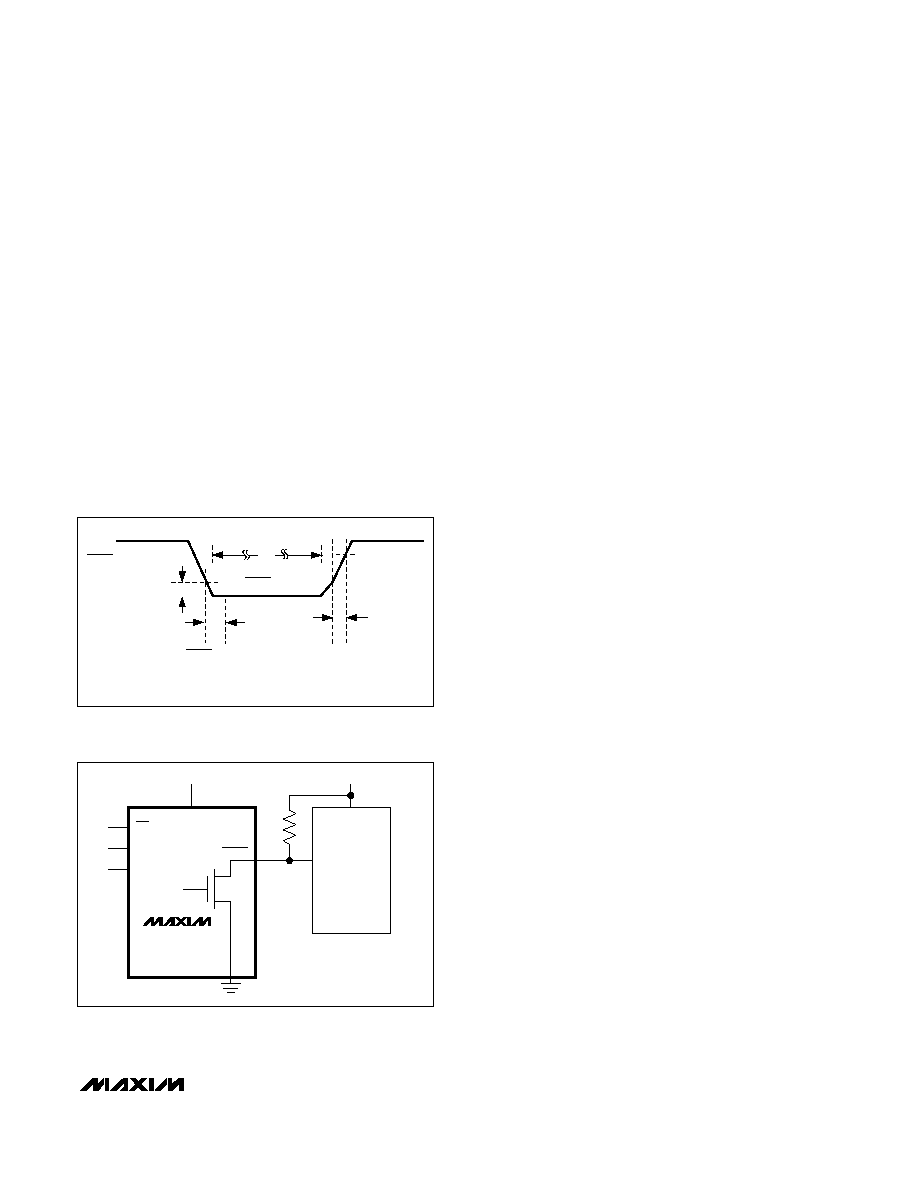
Reset Output
The MAX6316L/MAX6318LH/MAX6319LH feature an
active-low reset output, while the MAX6317H/
MAX6318_H/MAX6319_H/MAX6321HP/MAX6322HP
feature an active-high reset output. RESET is guaran-
teed to be a logic low and RESET is guaranteed to be a
logic high for V
CC
down to 1V.
The MAX6316MAX6322 assert reset when V
CC
is below
the reset threshold (V
RST
), when MR is pulled low
(MAX6316_/MAX6317H/MAX6319_H/MAX6320P/
MAX6322HP only), or if the WDI pin is not serviced within
the watchdog timeout period (t
WD
). Reset remains assert-
ed for the specified reset active timeout period (t
RP
) after
V
CC
rises above the reset threshold, after MR transitions
low to high, or after the watchdog timer asserts the reset
(MAX6316_/MAX6317H/MAX6318_H/MAX6320P/
MAX6321HP). After the reset active timeout period (t
RP
)
expires, the reset output deasserts, and the watchdog
timer restarts from zero (Figure 2).
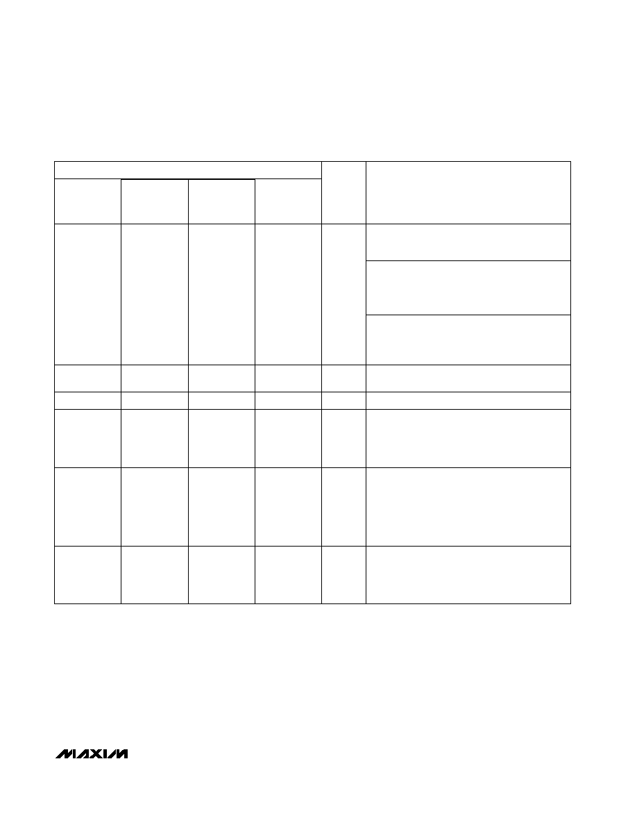
MAX6316MAX6322
V
CC
V
CC
WDI
(ALL EXCEPT
MAX6319/MAX6322)
1.23V
52k
52k
GND
RESET
(ALL EXCEPT
MAX6316/MAX6320P)
RESET
(ALL EXCEPT MAX6317)
MR
(ALL EXCEPT
MAX6318/MAX6321)
RESET
GENERATOR
WATCHDOG
TIMER
WATCHDOG
TRANSITION
DETECTOR
Figure 1. Functional Diagram
V
CC
1V
1V
t
RD
V
RST
V
RST
t
RD
RESET
GND
RESET
t
RP
t
RP
GND
Figure 2. Reset Timing Diagram
MAX6316MAX6322
5-Pin µP Supervisory Circuits with
Watchdog and Manual Reset
_______________________________________________________________________________________
7
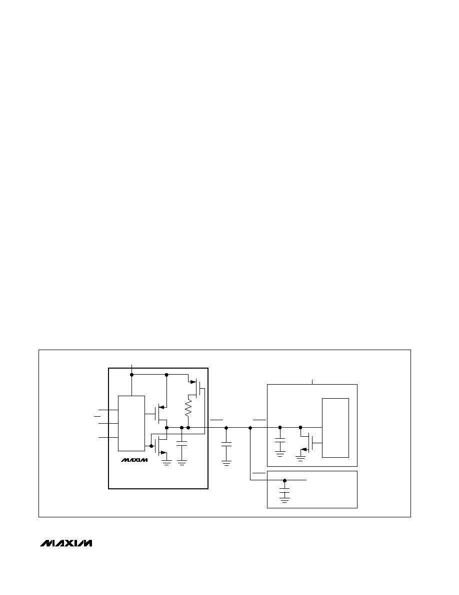
Bidirectional
R
RE
ES
SE
ET
T Output
The MAX6316M/MAX6318MH/MAX6319MH are designed
to interface with µPs that have bidirectional reset pins,
such as the Motorola 68HC11. Like an open-drain output,
these devices allow the µP or other devices to pull the
bidirectional reset (RESET) low and assert a reset condi-
tion. However, unlike a standard open-drain output, it
includes the commonly specified 4.7k
pullup resistor
with a P-channel active pullup in parallel.
This configuration allows the MAX6316M/MAX6318MH/
MAX6319MH to solve a problem associated with µPs
that have bidirectional reset pins in systems where sev-
eral devices connect to RESET (Figure 3). These µPs
can often determine if a reset was asserted by an exter-
nal device (i.e., the supervisor IC) or by the µP itself
(due to a watchdog fault, clock error, or other source),
and then jump to a vector appropriate for the source of
the reset. However, if the µP does assert reset, it does
not retain the information, but must determine the
cause after the reset has occurred.
The following procedure describes how this is done in
the Motorola 68HC11. In all cases of reset, the µP pulls
RESET low for about four external-clock cycles. It then
releases RESET, waits for two external-clock cycles,
then checks RESET's state. If RESET is still low, the µP
concludes that the source of the reset was external
and, when RESET eventually reaches the high state, it
jumps to the normal reset vector. In this case, stored-
state information is erased and processing begins from
scratch. If, on the other hand, RESET is high after a
delay of two external-clock cycles, the processor
knows that it caused the reset itself and can jump to a
different vector and use stored-state information to
determine what caused the reset.
A problem occurs with faster µPs; two external-clock
cycles are only 500ns at 4MHz. When there are several
devices on the reset line, and only a passive pullup resis-
tor is used, the input capacitance and stray capacitance
can prevent RESET from reaching the logic high state (0.8
V
CC
) in the time allowed. If this happens, all resets will
be interpreted as external. The µP output stage is guaran-
teed to sink 1.6mA, so the rise time can not be reduced
considerably by decreasing the 4.7k
internal pullup
resistance. See Bidirectional Pullup Characteristics in the
Typical Operating Characteristics.
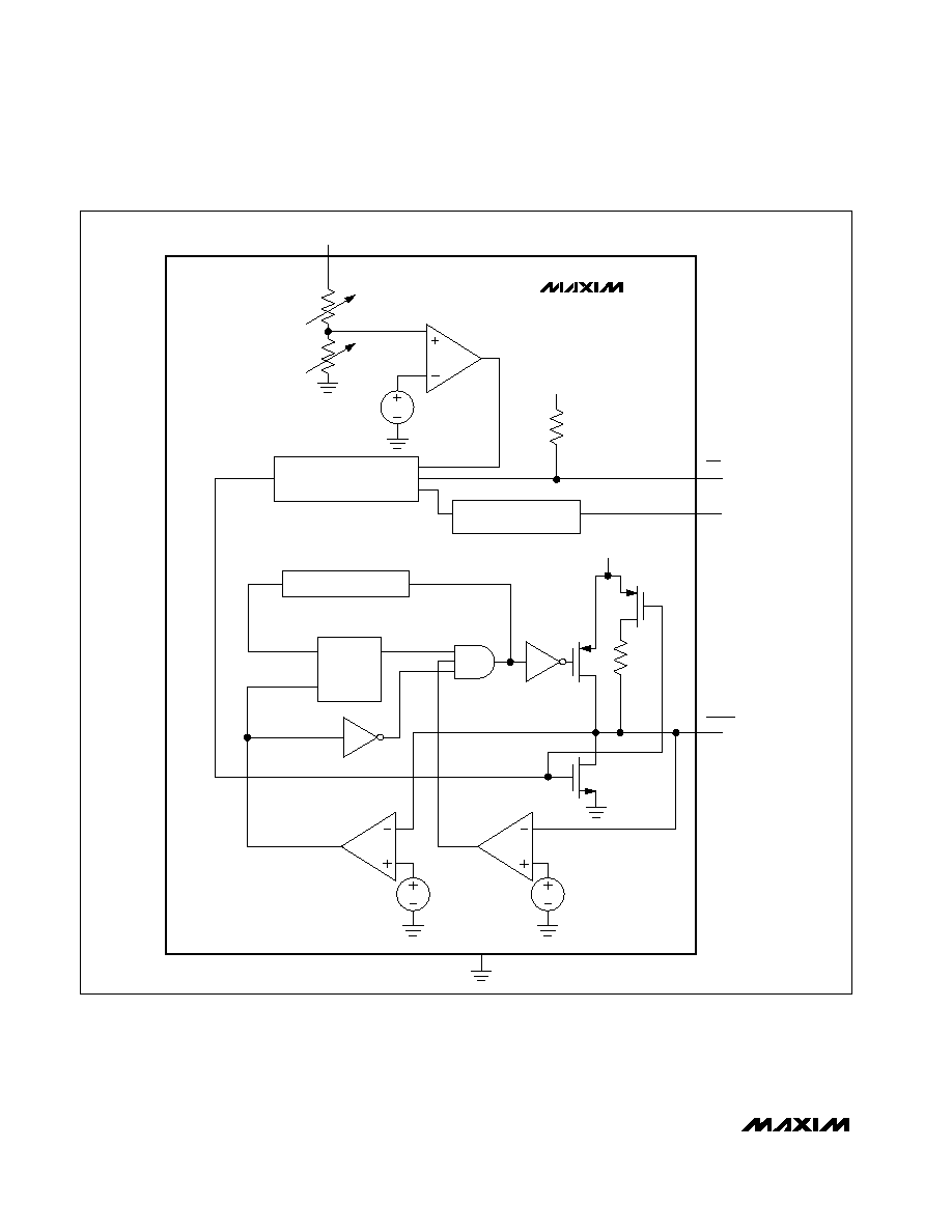
The MAX6316M/MAX6318MH/MAX6319MH overcome
this problem with an active pullup FET in parallel with the
4.7k
resistor (Figures 4 and 5). The pullup transistor
holds RESET high until the µP reset I/O or the supervisory
circuit itself forces the line low. Once RESET goes below
V
PTH
, a comparator sets the transition edge flip-flop, indi-
cating that the next transition for RESET will be low to
high. When RESET is released, the 4.7k
resistor pulls
RESET up toward V
CC
. Once RESET rises above V
PTH
but is below (0.85 x V
CC
), the active P-channel pullup
turns on. Once RESET rises above (0.85 x V
CC
) or the
2µs one-shot times out, the active pullup turns off. The
parallel combination of the 4.7k
pullup and the
4.7k
MR**
C
IN
RESET
RESET
CIRCUITRY
RESET***
WDI*
V
CC
MAX6316M
MAX6318MH
MAX6319MH
C
STRAY
68HC11
RESET
CIRCUITRY
C
IN
RESET
V
CC
OTHER DEVICES
C
IN
RESET
MAX6316M/MAX6318MH
MAX6316M/MAX6319MH
ACTIVE-HIGH PUSH/PULL MAX6318MH/MAX6319MH
*
**
***
Figure 3. MAX6316M/MAX6318MH/MAX6319MH Supports Additional Devices on the Reset Bus
MAX6316MAX6322
5-Pin µP Supervisory Circuits with
Watchdog and Manual Reset
8
_______________________________________________________________________________________
V
CC
MAX6316M
MAX6318MH
MAX6319MH
LASER-
TRIMMED
RESISTORS
VREF
V
CC
52k
MR
WDI
(MAX6316M/
MAX6318MH)
(MAX6316M/
MAX6319MH)
RESET
GENERATOR
2
µs ONE SHOT
2
µs ONE SHOT
WATCHDOG ON
CIRCUITRY
TRANSITION
FLIP-FLOP
R
Q
S
FF
V
CC
4.7k
RESET
ACTIVE PULLUP
ENABLE COMPARATOR
0.65V
0.85V
CC
GND
Figure 4. MAX6316/MAX6318MH/MAX6319MH Bidirectional Reset Output Functional Diagram
MAX6316MAX6322
5-Pin µP Supervisory Circuits with
Watchdog and Manual Reset
_______________________________________________________________________________________
9
P-channel transistor on-resistance quickly charges
stray capacitance on the reset line, allowing RESET to
transition from low to high within the required two elec-
tronic-clock cycles, even with several devices on the
reset line. This process occurs regardless of whether
the reset was caused by V
CC
dipping below the reset
threshold, the watchdog timing out, MR being asserted,
or the µP or other device asserting RESET. The parts do
not require an external pullup. To minimize supply cur-
rent consumption, the internal 4.7k
pullup resistor dis-
connects from the supply whenever the MAX6316M/
MAX6318MH/MAX6319MH assert reset.
Open-Drain
R
RE
ES
SE
ET
T Output
The MAX6320P/MAX6321HP/MAX6322HP have an
active-low, open-drain reset output. This output struc-
ture will sink current when RESET is asserted. Connect
a pullup resistor from RESET to any supply voltage up
to 6V (Figure 6). Select a resistor value large enough to
register a logic low (see Electrical Characteristics), and
small enough to register a logic high while supplying all
input current and leakage paths connected to the RESET
line. A 10k
pullup is sufficient in most applications.
Manual-Reset Input
The MAX6316_/MAX6317H/MAX6319_H/MAX6320P/
MAX6322HP feature a manual reset input. A logic low on
MR asserts a reset. After MR transitions low to high, reset
remains asserted for the duration of the reset timeout peri-
od (t
RP
). The MR input is connected to V
CC
through an
internal 52k
pullup resistor and therefore can be left
unconnected when not in use. MR can be driven with
TTL-logic levels in 5V systems, with CMOS-logic levels in
3V systems, or with open-drain or open-collector output
devices. A normally-open momentary switch from MR to
ground can also be used; it requires no external
debouncing circuitry. MR is designed to reject fast,
negative-going transients (typically 100ns pulses). A
0.1µF capacitor from MR to ground provides additional
noise immunity.
The MR input pin is equipped with internal ESD-protection
circuitry that may become forward biased. Should MR be
driven by voltages higher than V
CC
, excessive current
would be drawn, which would damage the part. For
example, assume that MR is driven by a +5V supply other
than V
CC
. If V
CC
drops lower than +4.7V, MR's absolute
maximum rating is violated [-0.3V to (V
CC
+ 0.3V)], and
undesirable current flows through the ESD structure from
MR to V
CC
. To avoid this, use the same supply for MR as
the supply monitored by V
CC
. This guarantees that the
voltage at MR will never exceed V
CC
.
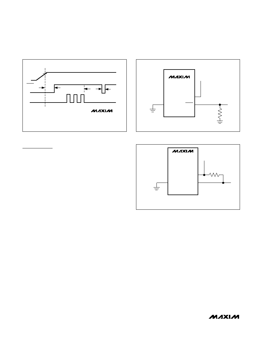
Watchdog Input
The MAX6316_/MAX6317H/MAX6318_H/MAX6320P/
MAX6321HP feature a watchdog circuit that monitors
the µP's activity. If the µP does not toggle the watchdog
input (WDI) within the watchdog timeout period (t
WD
),
reset asserts. The internal watchdog timer is cleared by
reset or by a transition at WDI (which can detect pulses
as short as 50ns). The watchdog timer remains cleared
while reset is asserted. Once reset is released, the
timer begins counting again (Figure 7).
The WDI input is designed for a three-stated output
device with a 10µA maximum leakage current and the
capability of driving a maximum capacitive load of 200pF.
The three-state device must be able to source and sink at
least 200µA when active. Disable the watchdog function
by leaving WDI unconnected or by three-stating the driver
connected to WDI. When the watchdog timer is left open
circuited, the timer is cleared internally at intervals equal
to 7/8 of the watchdog period.
MAX6320
MAX6321
MAX6322
V
CC
GND
RESET
WDI**
MR*
RESET***
MAX6320/MAX6322
MAX6320/MAX6321
MAX6321/MAX6322
*
**
***
5V SYSTEM
+5.0V
+3.3V
10k
Figure 6. MAX6320P/MAX6321HP/MAX6322HP Open-Drain
RESET Output Allows Use with Multiple Supplies
t
R
t
S
RESET
RESET PULLED LOW
BY
µC OR
RESET GENERATOR
ACTIVE
PULLUP
TURNS ON
V
CC
0.7V
0.8 x V
CC
t
RP
OR
µC RESET DELAY
Figure 5. Bidirectional RESET Timing Diagram
MAX6316MAX6322
5-Pin µP Supervisory Circuits with
Watchdog and Manual Reset
10
______________________________________________________________________________________
Applications Information
Watchdog Input Current
The WDI input is internally driven through a buffer and
series resistor from the watchdog counter. For minimum
watchdog input current (minimum overall power con-
sumption), leave WDI low for the majority of the watch-
dog timeout period. When high, WDI can draw as much
as 160µA. Pulsing WDI high at a low duty cycle will
reduce the effect of the large input current. When WDI
is left unconnected, the watchdog timer is serviced
within the watchdog timeout period by a low-high-low
pulse from the counter chain.
Negative-Going V
CC
Transients
These supervisors are immune to short-duration, nega-
tive-going V
CC
transients (glitches), which usually do
not require the entire system to shut down. Typically,
200ns large-amplitude pulses (from ground to V
CC
) on
the supply will not cause a reset. Lower amplitude puls-
es result in greater immunity. Typically, a V
CC
transient
that goes 100mV under the reset threshold and lasts
less than 4µs will not trigger a reset. An optional 0.1µF
bypass capacitor mounted close to V
CC
provides addi-
tional transient immunity.
Ensuring Valid Reset Outputs
Down to V
CC
= 0
The MAX6316_/MAX6317H/MAX6318_H/MAX6319_H/
MAX6321HP/MAX6322HP are guaranteed to operate
properly down to V
CC
= 1V. In applications that require
valid reset levels down to V
CC
= 0, a pulldown resistor
to active-low outputs (push/pull and bidirectional only,
Figure 8) and a pullup resistor to active-high outputs
(push/pull only, Figure 9) will ensure that the reset line
is valid while the reset output can no longer sink or
source current. This scheme does not work with the
open-drain outputs of the MAX6320/MAX6321/MAX6322.
The resistor value used is not critical, but it must be
large enough not to load the reset output when V
CC
is
above the reset threshold. For most applications,
100k
is adequate.
Watchdog Software Considerations
(MAX6316/MAX6317/MAX6318/
MAX6320/MAX6321)
One way to help the watchdog timer monitor software
execution more closely is to set and reset the watchdog
input at different points in the program, rather than
pulsing the watchdog input high-low-high or low-high-
low. This technique avoids a stuck loop, in which the
watchdog timer would continue to be reset inside the
loop, keeping the watchdog from timing out.
V
CC
t
WD
t
RP
t
RP
t
RST
WDI
RESET
MAX6316/MAX6317
MAX6318/MAX6320
MAX6321
Figure 7. Watchdog Timing Relationship
GND
*THIS SCHEMATIC DOES NOT WORK ON THE OPEN-DRAIN
OUTPUTS OF THE MAX6321/MAX6322.
100k
V
CC
V
CC
RESET
MAX6317
MAX6318
MAX6319
MAX6321*
MAX6322*
Figure 9. Ensuring RESET Valid to V
CC
= 0 on Active-High
Push/Pull Outputs
GND
100k
V
CC
V
CC
RESET
MAX6316
MAX6318
MAX6319
Figure 8. Ensuring RESET Valid to V
CC
= 0 on Active-Low
Push/Pull and Bidirectional Outputs
MAX6316MAX6322
5-Pin µP Supervisory Circuits with
Watchdog and Manual Reset
______________________________________________________________________________________
11
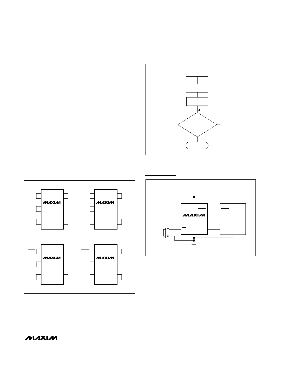
Figure 10 shows an example of a flow diagram where
the I/O driving the watchdog input is set high at the
beginning of the program, set low at the end of every
subroutine or loop, then set high again when the pro-
gram returns to the beginning. If the program should
hang in any subroutine, the problem would be quickly
corrected, since the I/O is continually set low and the
watchdog timer is allowed to time out, causing a reset
or interrupt to be issued. As described in the Watchdog
Input Current section, this scheme results in higher time
average WDI current than does leaving WDI low for the
majority of the timeout period and periodically pulsing it
low-high-low.
START
SET WDI
HIGH
PROGRAM
CODE
SUBROUTINE OR
PROGRAM LOOP
SET WDI LOW
RETURN
POSSIBLE
INFINITE LOOP PATH
Figure 10. Watchdog Flow Diagram
GND
WDI
MR
1
5 V
CC
RESET
MAX6316
MAX6320
SOT23-5
TOP VIEW
2
3
4
GND
WDI
MR
1
5 V
CC
RESET
MAX6317
SOT23-5
2
3
4
GND
WDI
RESET
1
5 V
CC
RESET
MAX6318
MAX6321
SOT23-5
2
3
4
GND
MR
RESET
1
5 V
CC
RESET
MAX6319
MAX6322
SOT23-5
2
3
4
__________________Pin Configurations
MAX6316
GND
MANUAL
RESET
I/O
WDI
MR
GND
µP
V
CC
V
IN
V
CC
RESET
RESET
Typical Operating Circuit
Table 2. Standard Versions
Table 1. Factory-Trimmed Reset Thresholds
MAX6316MAX6322
5-Pin µP Supervisory Circuits with
Watchdog and Manual Reset
12
______________________________________________________________________________________
2.438
2.563
2.463
2.500
2.538
MAX63___25_ _-T
2.564
2.696
2.591
2.630
2.669
MAX63___26_ _-T
2.633
2.768
2.660
2.700
2.741
MAX63___27_ _-T
2.730
2.870
2.758
2.800
2.842
MAX63___28_ _-T
2.857
3.000
2.886
2.930
2.974
MAX63___29_ _-T
2.925
3.075
2.955
3.000
3.045
MAX63___30_ _-T
3.003
3.157
3.034
3.080
3.126
MAX63___31_ _-T
3.120
3.280
3.152
3.200
3.248
MAX63___32_ _-T
3.218
3.383
3.251
3.300
3.350
MAX63___33_ _-T
3.315
3.485
3.349
3.400
3.451
MAX63___34_ _-T
3.413
3.588
3.448
3.500
3.553
MAX63___35_ _-T
3.510
3.690
3.546
3.600
3.654
MAX63___36_ _-T
3.608
3.793
3.645
3.700
3.756
MAX63___37_ _-T
3.705
3.895
3.743
3.800
3.857
MAX63___38_ _-T
3.803
3.998
3.842
3.900
3.959
MAX63___39_ _-T
3.900
4.100
3.940
4.000
4.060
MAX63___40_ _-T
3.998
4.203
4.039
4.100
4.162
MAX63___41_ _-T
4.095
4.305
4.137
4.200
4.263
MAX63___42_ _-T
4.193
4.408
4.236
4.300
4.365
MAX63___43_ _-T
4.270
4.490
4.314
4.390
4.446
MAX63___44_ _-T
4.388
4.613
4.433
4.500
4.568
MAX63___45_ _-T
4.514
4.746
4.561
4.630
4.699
MAX63___46_ _-T
4.583
4.818
4.630
4.700
4.771
MAX63___47_ _-T
4.680
4.920
4.728
4.800
4.872
MAX63___48_ _-T
4.778
5.023
7.827
4.900
4.974
MAX63___49_ _-T
MIN
MAX
MIN
TYP
MAX
4.875
5.125
T
A
= -40°C to +85°C
T
A
= +25°C
4.925
5.000
5.075
MAX63___50_ _-T
PART
PART
RESET
THRESHOLD (V)
MINIMUM
RESET
TIMEOUT (ms)
TYPICAL
WATCHDOG
TIMEOUTS (s)
SOT
TOP
MARK
MAX6316LUK29CY-T
2.93
140
1.6
ACDE
MAX6316LUK46CY-T
4.63
140
1.6
ACDD
MAX6316MUK29CY-T
2.93
140
1.6
ACDG
MAX6316MUK46CY-T
4.63
140
1.6
ACDF
MAX6317HUK46CY-T
4.63
140
1.6
ACDQ
MAX6318LHUK46CY-T
4.63
140
1.6
ACDH
MAX6318MHUK46CY-T
4.63
140
1.6
ACDJ
MAX6319LHUK46C-T
4.63
140
--
ACDK
MAX6319MHUK46C-T
4.63
140
--
ACDM
MAX6320PUK29CY-T
2.93
140
1.6
ACDO
Table 3. Reset/Watchdog Timeout Periods
MAX6316MAX6322
5-Pin µP Supervisory Circuits with
Watchdog and Manual Reset
______________________________________________________________________________________
13
__Ordering Information (continued)
Note: These devices are available with factory-set V
CC
reset
thresholds from 2.5V to 5V, in 0.1V increments. Insert the
desired nominal reset threshold (25 to 50, from Table 1) into the
blanks following the letters UK. All devices offer factory-pro-
grammed reset timeout periods. Insert the letter corresponding
to the desired reset timeout period (A, B, C, or D from Table 3)
into the blank following the reset threshold suffix. Parts that offer
a watchdog feature (see Selector Guide) are factory-trimmed to
one of four watchdog timeout periods. Insert the letter corre-
sponding to the desired watchdog timeout period (W, X, Y, or Z
from Table 3) into the blank following the reset timeout suffix.
PART
MAX6319LHUK____-T
MAX6319MHUK____-T
MAX6320PUK____-T
-40°C to +85°C
-40°C to +85°C
-40°C to +85°C
TEMP RANGE
PIN-PACKAGE
5 SOT23-5
5 SOT23-5
5 SOT23-5
MAX6321HPUK____-T
-40°C to +85°C
5 SOT23-5
MAX6322HPUK____-T
-40°C to +85°C
5 SOT23-5
W
4.3
6.3
9.3
ms
X
71
102
153
Y
1.12
1.6
2.4
Z
17.9
25.6
38.4
s
RESET TIMEOUT PERIODS
WATCHDOG TIMEOUT
TRANSISTOR COUNT: 191
SUBSTRATE IS INTERNALLY CONNECTED TO V+
Chip Information
s
2.24
1.60
1.12
D
280
200
140
C
40
30
20
B
2
1.6
1
A
UNITS
MAX
TYP
MIN
SUFFIX
ms
Note: Thirteen standard versions are available, with a required order increment of 2500 pieces. Sample stock is generally held on stan-
dard versions only. The required order increment for nonstandard versions is 10,000 pieces. Contact factory for availability.
PART
RESET
THRESHOLD (V)
MINIMUM
RESET
TIMEOUT (ms)
TYPICAL
WATCHDOG
TIMEOUTS (s)
SOT
TOP
MARK
MAX6320PUK46CY-T
4.63
140
1.6
ACDN
MAX6321HPUK46CY-T
4.63
140
1.6
ACGL
MAX6322HPUK46C-T
4.63
140
1.6
ACGN
Table 2. Standard Versions (continued)
MAX6316MAX6322
5-Pin µP Supervisory Circuits with
Watchdog and Manual Reset
Maxim cannot assume responsibility for use of any circuitry other than circuitry entirely embodied in a Maxim product. No circuit patent licenses are
implied. Maxim reserves the right to change the circuitry and specifications without notice at any time.
14 ____________________Maxim Integrated Products, 120 San Gabriel Drive, Sunnyvale, CA 94086 408-737-7600
© 2002 Maxim Integrated Products
Printed USA
is a registered trademark of Maxim Integrated Products.
SOT5L.EPS
Package Information
(The package drawing(s) in this data sheet may not reflect the most current specifications. For the latest package outline information
go to www.maxim-ic.com/packages.)