
___________________________________________________________________Selector Guide
For free samples & the latest literature: http://www.maxim-ic.com, or phone 1-800-998-8800.
For small orders, phone 1-800-835-8769.
________________General Description
The MAX6316≠MAX6322 family of microprocessor (µP)
supervisory circuits monitors power supplies and
microprocessor activity in digital systems. It offers sev-
eral combinations of push/pull, open-drain, and bidirec-
tional (such as Motorola 68HC11) reset outputs, along
with watchdog and manual-reset features. The
Selector
Guide below lists the specific functions available from
each device. These devices are specifically designed
to ignore fast negative transients on V
CC
. Resets are
guaranteed valid for V
CC
down to 1V.
These devices are available in 26 factory-trimmed reset
threshold voltages (from 2.5V to 5V, in 100mV incre-
ments), featuring four minimum power-on reset timeout
periods (from 1ms to 1.12sec), and four watchdog time-
out periods (from 6.3ms to 25.6sec). Nine standard ver-
sions are available with an order increment requirement
of 2500 pieces (see
Standard Versions table); contact
the factory for availability of other versions, which have
an order increment requirement of 10,000 pieces.
The MAX6316≠MAX6322 are offered in a miniature
5-pin SOT23 package.
________________________Applications
Portable Computers
Computers
Controllers
Intelligent Instruments
Portable/Battery-Powered Equipment
Embedded Control Systems
____________________________Features
o
Small 5-Pin SOT23 Package
o
Available in 26 Reset Threshold Voltages
2.5V to 5V, in 100mV Increments
o
Four Reset Timeout Periods
1ms, 20ms, 140ms, or 1.12sec (min)
o
Four Watchdog Timeout Periods
6.3ms, 102ms, 1.6sec, or 25.6sec (typ)
o
Four Reset Output Stages
Active-High, Push/Pull
Active-Low, Push/Pull
Active-Low, Open-Drain
Active-Low, Bidirectional
o
Guaranteed Reset Valid to V
CC
= 1V
o
Immune to Short Negative V
CC
Transients
o
Low Cost
o
No External Components
MAX6316≠MAX6322
5-Pin µP Supervisory Circuits with
Watchdog and Manual Reset
________________________________________________________________
Maxim Integrated Products
1
19-0496; Rev 3; 1/99
PART
MAX6316
LUK____-T
MAX6316MUK____-T
-40∞C to +85∞C
-40∞C to +85∞C
TEMP. RANGE
PIN-PACKAGE
5 SOT23-5
5 SOT23-5
_______________Ordering Information
Ordering Information continued at end of data sheet.
MAX6317
HUK____-T
-40∞C to +85∞C
5 SOT23-5
MAX6318
HUK____-T
-40∞C to +85∞C
5 SOT23-5
ACTIVE-LOW
OPEN-DRAIN
MAX6316L
MAX6316M
MAX6317H
MAX6321HP
MAX6318LH
--
MAX6318MH**
--
MAX6319LH
--
MAX6319MH**
--
MAX6320P
ACTIVE-LOW
PUSH/PULL
--
--
--
--
--
ACTIVE-HIGH
PUSH/PULL
--
--
--
ACTIVE-LOW
BIDIRECTIONAL
--
--
--
--
--
PART
WATCHDOG
INPUT
MANUAL
RESET
INPUT
--
--
--
--
MAX6322HP
--
--
--
--
--
--
--
RESET OUTPUTS*
--
--
*
The MAX6318/MAX6319/MAX6321/MAX6322 feature two types of reset output on each device.
**
Future product--contact factory for availability.
MAX6318MHUK____-T
-40∞C to +85∞C
5 SOT23-5
Typical Operating Circuit and Pin Configurations appear at
end of data sheet.
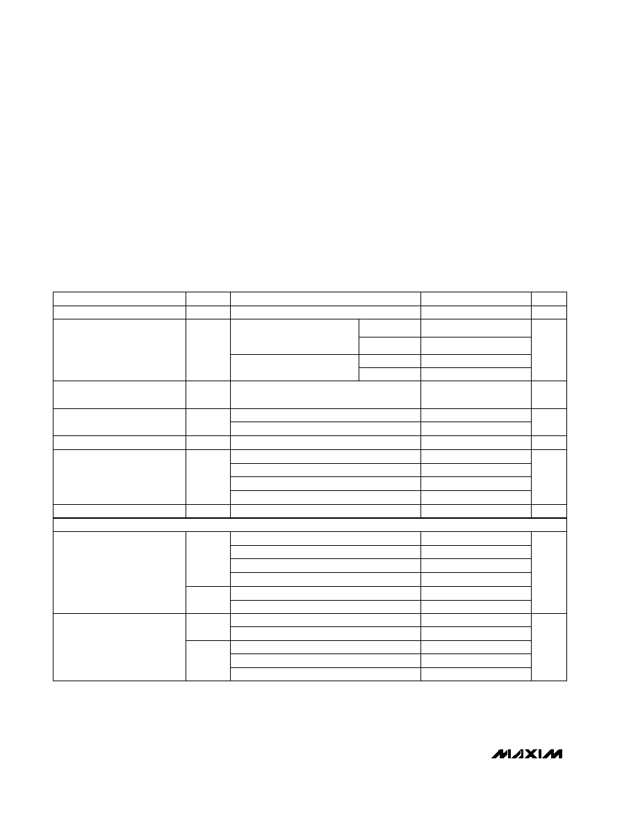
ELECTRICAL CHARACTERISTICS
(V
CC
= 2.5V to 5.5V, T
A
= -40∞C to +85∞C, unless otherwise noted. Typical values are at T
A
= +25∞C.) (Note 1)
MAX6316≠MAX6322
5-Pin µP Supervisory Circuits with
Watchdog and Manual Reset
2
_______________________________________________________________________________________
ABSOLUTE MAXIMUM RATINGS
Stresses beyond those listed under "Absolute Maximum Ratings" may cause permanent damage to the device. These are stress ratings only, and functional
operation of the device at these or any other conditions beyond those indicated in the operational sections of the specifications is not implied. Exposure to
absolute maximum rating conditions for extended periods may affect device reliability.
Voltage (with respect to GND)
V
CC
......................................................................-0.3V to +6V
RESET (MAX6320/MAX6321/MAX6322 only)...... -0.3V to +6V
All Other Pins.........................................-0.3V to (V
CC
+ 0.3V)
Input/Output Current, All Pins .............................................20mA
Continuous Power Dissipation (T
A
= +70∞C)
SOT23-5 (derate 7.1mW/∞C above +70∞C)...............571mW
Operating Temperature Range............................-40∞C to +85∞C
Junction Temperature ......................................................+150∞C
Storage Temperature Range..............................-65∞C to +160∞C
Lead Temperature (soldering, 10sec)..............................+300∞C
V
CC
- 1.5
0.8 x V
CC
V
OH
0.4
0.3
0.3
V
0.3
V
OL
RESET Output Voltage
µs
40
t
RD
V
CC
to RESET Delay
1120
1600
2240
140
200
280
20
28
40
ms
1
1.4
2
t
RP
Reset Active Timeout Period
mV
3
Reset Threshold Hysteresis
V
1
5.5
V
CC
Operating Voltage Range
V
TH
-2.5% V
TH
V
TH
+2.5%
V
V
TH
-1.5% V
TH
V
TH
+1.5%
V
RST
Reset Threshold (Note 2)
ppm/∞C
40
V
TH
/∞C
Reset Threshold Temperature
Coefficient
UNITS
MIN
TYP
MAX
SYMBOL
PARAMETER
V
CC
4.5V, I
SOURCE
= 800µA
V
CC
2.7V, I
SOURCE
= 500µA
V
CC
4.5V, I
SINK
= 3.2mA
V
CC
2.7V, I
SINK
= 1.2mA
V
CC
1.2V, I
SINK
= 100µA
V
CC
1.0V, I
SINK
= 50µA
T
A
= -40∞C to +85∞C
V
CC
falling at 1mV/µs
MAX63_ _D_-T
T
A
= -40∞C to +85∞C
T
A
= +25∞C
MAX63_ _C_-T
MAX63_ _B_-T
MAX63_ _A_-T
CONDITIONS
V
0.3
V
OL
RESET Output Voltage
V
CC
2.7V, I
SINK
= 1.2mA
0.4
V
CC
4.5V, I
SINK
= 3.2mA
0.8 x V
CC
V
OH
V
CC
1.8V, I
SOURCE
= 150µA
0.8 x V
CC
V
CC
2.7V, I
SOURCE
= 500µA
V
CC
- 1.5
V
CC
4.5V, I
SOURCE
= 800µA
Note 1:
Over-temperature limits are guaranteed by design, not production tested.
Note 2:
A factory-trimmed voltage divider programs the nominal reset threshold (V
TH
). Factory-trimmed reset thresholds are
available in 100mV increments from 2.5V to 5V (see Table 1 at end of data sheet).
MAX6316/MAX6317/MAX6318/
MAX6320/MAX6321:
MR and WDI unconnected
µA
10
20
I
CC
Supply Current
V
CC
= 5.5V
5
12
V
CC
= 3.6V
MAX6319/MAX6322:
MR unconnected
5
12
V
CC
= 5.5V
3
8
V
CC
= 3.6V
PUSH/PULL RESET OUTPUT (MAX6316L/MAX6317H/MAX6318_H/MAX6319_H/MAX6321HP/MAX6322HP)

MAX6316≠MAX6322
5-Pin µP Supervisory Circuits with
Watchdog and Manual Reset
_______________________________________________________________________________________
3
Note 3:
This is the minimum time RESET must be held low by an external pull-down source to set the active pull-up flip-flop.
Note 4:
Measured from RESET V
OL
to (0.8 x V
CC
), R
LOAD
=
.
Note 5:
WDI is internally serviced within the watchdog period if WDI is left unconnected.
Note 6:
The WDI input current is specified as the average input current when the WDI input is driven high or low. The WDI input is
designed for a three-stated-output device with a 10µA maximum leakage current and capable of driving a maximum capaci-
tive load of 200pF. The three-state device must be able to source and sink at least 200µA when active.
µA
1.0
I
LKG
Open-Drain Reset Output
Leakage Current
ns
400
t
S
Transition Flip-Flop Setup Time
333
ns
333
t
R
RESET Output Rise Time
(Note 4)
UNITS
MIN
TYP
MAX
SYMBOL
PARAMETER
(Note 3)
V
CC
= 5.0V, C
L
= 200pF
V
CC
= 3.0V, C
L
= 120pF
CONDITIONS
ELECTRICAL CHARACTERISTICS (continued)
(V
CC
= 2.5V to 5.5V, T
A
= -40∞C to +85∞C, unless otherwise noted. Typical values are at T
A
= +25∞C.) (Note 1)
666
666
V
CC
= 5.0V, C
L
= 400pF
V
CC
= 3.0V, C
L
= 250pF
V
0.4
0.65
V
PTH
Active Pull-Up Enable Threshold
V
CC
= 5.0V
mA
20
RESET Active Pull-Up Current
V
CC
= 5.0V
k
4.2
4.7
5.2
RESET Pull-Up Resistance
V
0.3
V
OL
RESET Output Voltage
V
CC
1.0V, I
SINK
= 50µA
0.3
V
CC
1.2V, I
SINK
= 100µA
0.3
V
CC
2.7V, I
SINK
= 1.2mA
0.4
V
CC
4.5V, I
SINK
= 3.2mA
ms
4.3
6.3
9.3
t
WD
Watchdog Timeout Period
MAX63_ _ _ W-T
71
102
153
MAX63_ _ _ X-T
sec
1.12
1.6
2.4
MAX63_ _ _ Y-T
17.9
25.6
38.4
MAX63_ _ _ Z-T
ns
50
t
WDI
WDI Pulse Width
V
IL
= 0.3 x V
CC
, V
IH
= 0.7 x V
CC
V
0.3 x V
CC
V
IL
WDI Input Threshold
(Note 5)
0.7 x V
CC
120
160
I
WDI
WDI Input Current
(Note 6)
WDI = V
CC
, time average
-20
-15
V
WDI
= 0, time average
V
IH
V
0.8
V
IL
MR Input Threshold
V
TH
> 4.0V
2.0
V
IH
0.3 x V
CC
V
IL
V
TH
< 4.0V
0.7 x V
CC
V
IH
µs
1
MR Input Pulse Width
ns
100
MR Glitch Rejection
k
35
52
75
MR Pull-Up Resistance
ns
230
MR to Reset Delay
V
CC
= 5V
µA
BIDIRECTIONAL
RESET
OUTPUT (MAX6316M/MAX6318MH/MAX6319MH)
OPEN-DRAIN
RESET
OUTPUT (MAX6320P/MAX6321HP/MAX6322HP)
WATCHDOG INPUT (MAX6316/MAX6317H/MAX6318_H/MAX6320P/MAX6321HP)
MANUAL-RESET INPUT (MAX6316_/MAX6317H/MAX6319_H/MAX6320P/MAX6322HP)
MAX6316≠MAX6322
5-Pin µP Supervisory Circuits with
Watchdog and Manual Reset
4
_______________________________________________________________________________________
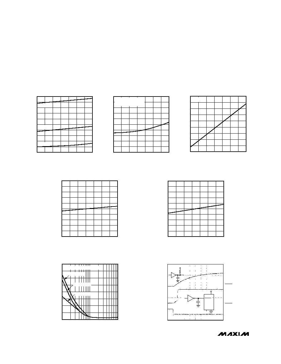
__________________________________________Typical Operating Characteristics
(T
A
= +25∞C, unless otherwise noted.)
0
2
1
4
3
8
7
6
5
10
9
-40
0
20
-20
40
60
80
100
MAX6316/17/18/20/21
SUPPLY CURRENT vs. TEMPERATURE
MAX6316toc01
TEMPERATURE (∞C)
SUPPLY CURRENT (
µ
A)
V
CC
= 5V
V
CC
= 3V
V
CC
= 1V
0
30
20
10
50
40
90
80
70
60
100
-40
-20
0
20
40
60
80
100
V
CC
FALLING TO RESET PROPAGATION
DELAY vs. TEMPERATURE
MAX6316toc03
TEMPERATURE (∞C)
RESET PROPAGATION DELAY (
µ
s)
V
CC
FALLING AT 1mV/
µ
s
V
RST
- V
CC
= 100mV
140
180
160
240
220
200
300
280
260
320
-40
0
20
-20
40
60
80
100
MAX6316/17/19/20/22
MANUAL-RESET TO RESET
PROPAGATION DELAY vs. TEMPERATURE
MAX6316toc04
TEMPERATURE (∞C)
PROPAGATION DELAY (ns)
V
CC
= 5V
0.95
0.98
0.97
0.96
1.00
0.99
1.04
1.03
1.02
1.01
1.05
-40
-20
0
20
40
60
80
100
NORMALIZED RESET TIMEOUT
PERIOD vs. TEMPERATURE
MAX6316toc05
TEMPERATURE (∞C)
NORMALIZED RESET TIMEOUT PERIOD
0.95
0.98
0.97
0.96
1.00
0.99
1.04
1.03
1.02
1.01
1.05
-40
-20
0
20
40
60
80
100
MAX6316/17/18/20/21
NORMALIZED WATCHDOG TIMEOUT
PERIOD vs. TEMPERATURE
MAX6316toc06
TEMPERATURE (∞C)
NORMALIZED WATCHDOG TIMEOUT PERIOD
80
0
10
100
1000
MAXIMUM V
CC
TRANSIENT DURATION
vs. RESET THRESHOLD OVERDRIVE
20
10
MAX6316toc08
RESET THRESHOLD OVERDRIVE (mV) V
RST
- V
CC
TRANSIENT DURATION (
µ
s)
30
50
60
40
70
V
RST
= 3.3V
V
RST
= 4.63V
V
RST
= 2.63V
RESET OCCURS ABOVE LINES
PASSIVE
4.7k
PULL-UP
2V/div
RESET, ACTIVE
PULL-UP
2V/div
RESET
INPUT
5V/div
200ns/div
MAX6316M/6318MH/6319MH
BIDIRECTIONAL
PULL-UP CHARACTERISTICS
MAX6316toc09
100pF
4.7k
+5V
74HC05
74HC05
V
CC
GND
MR
100pF
INPUT
INPUT
+5V
RESET
MAX6316≠MAX6322
5-Pin µP Supervisory Circuits with
Watchdog and Manual Reset
_______________________________________________________________________________________
5
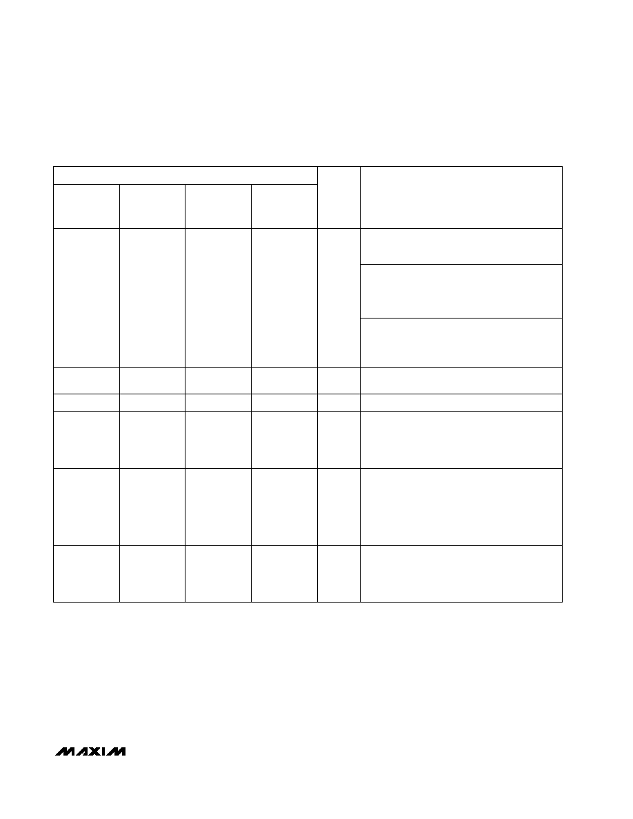
______________________________________________________________Pin Description
1
1
--
MAX6316M/MAX6318MH/MAX6319MH:
Bidirectional, Active-Low, Reset Output.
Intended to interface directly to microprocessors
with bidirectional resets such as the Motorola
68HC11.
MAX6320P/MAX6321HP/MAX6322HP:
Open-Drain, Active-Low, Reset Output. NMOS out-
put (sinks current only). Connect a pull-up resistor
from RESET to any supply voltage up to 6V.
MAX6316L/MAX6318LH/MAX6319LH:
Active-Low, Reset Output. CMOS push/pull
output (sources and sinks current).
RESET
1
4
--
5
3
2
MAX6319LH
MAX6319MH
MAX6322HP
PIN
--
4
5
3
2
MAX6318LH
MAX6318MH
MAX6321HP
3
4
5
1
2
MAX6317H
Active-Low, Manual Reset Input. Pull low to force a
reset. Reset remains asserted for the duration of
the Reset Timeout Period after MR transitions from
low to high. Leave unconnected or connected to
V
CC
if not used.
MR
3
Watchdog Input. Triggers a reset if it remains
either high or low for the duration of the watchdog
timeout period. The internal watchdog timer clears
whenever a reset asserts or whenever WDI sees a
rising or falling edge. To disable the watchdog fea-
ture, leave WDI unconnected or three-state the dri-
ver connected to WDI.
WDI
4
Supply Voltage. Reset is asserted when V
CC
drops below the Reset Threshold Voltage (V
RST
).
Reset remains asserted until V
CC
rises above
V
RST
and for the duration of the Reset Timeout
Period (t
RP
) once V
CC
rises above V
RST
.
V
CC
5
Active-High, Reset Output. CMOS push/pull output
(sources and sinks current). Inverse of RESET.
RESET
--
Ground
GND
2
MAX6316L
MAX6316M
MAX6320P
FUNCTION
NAME