 | –≠–ª–µ–∫—Ç—Ä–æ–Ω–Ω—ã–π –∫–æ–º–ø–æ–Ω–µ–Ω—Ç: MAX6426 | –°–∫–∞—á–∞—Ç—å:  PDF PDF  ZIP ZIP |
General Description
The MAX6340/MAX6421≠MAX6426 low-power micro-
processor supervisor circuits monitor system voltages
from 1.6V to 5V. These devices perform a single function:
they assert a reset signal whenever the V
CC
supply volt-
age falls below its reset threshold. The reset output
remains asserted for the reset timeout period after V
CC
rises above the reset threshold. The reset timeout is exter-
nally set by a capacitor to provide more flexibility.
The MAX6421/MAX6424 have an active-low, push-
pull reset output. The MAX6422 has an active-high,
push-pull reset output and the MAX6340/MAX6423/
MAX6425/MAX6426 have an active-low, open-drain
reset output. The MAX6421/MAX6422/MAX6423 are
offered in 4-pin SC70 or SOT143 packages. The
MAX6340/MAX6424/MAX6425/MAX6426 are available
in 5-pin SOT23-5 packages.
Applications
Portable Equipment
Battery-Powered Computers/Controllers
Automotive
Medical Equipment
Intelligent Instruments
Embedded Controllers
Critical µP Monitoring
Set-Top Boxes
Computers
Features
o Monitor System Voltages from 1.6V to 5V
o Capacitor-Adjustable Reset Timeout Period
o Low Quiescent Current (1.6µA typ)
o Three RESET Output Options
Push-Pull RESET
Push-Pull RESET
Open-Drain RESET
o Guaranteed Reset Valid to V
CC
= 1V
o Immune to Short V
CC
Transients
o Small 4-Pin SC70, 4-Pin SOT143, and 5-Pin SOT23
Packages
o MAX6340 Pin Compatible with LP3470
o MAX6424/MAX6425 Pin Compatible with
NCP300≠NCP303, MC33464/MC33465,
S807/S808/S809, and RN5VD
o MAX6426 Pin Compatible with PST92XX
MAX6340/MAX6421≠MAX6426
Low-Power, SC70/SOT µP Reset Circuits with
Capacitor-Adjustable Reset Timeout Delay
________________________________________________________________ Maxim Integrated Products
1
Ordering Information
GND
( ) ARE FOR THE MAX6422
V
CC
1
4
SRT
MAX6421X
MAX6422X
MAX6423X
SC70
TOP VIEW
2
3
RESET
(RESET)
Pin Configurations
19-2440; Rev 2; 10/02
For pricing, delivery, and ordering information, please contact Maxim/Dallas Direct! at
1-888-629-4642, or visit Maxim's website at www.maxim-ic.com.
Typical Operating Circuit appears at end of data sheet.
Selector Guide appears at end of data sheet.
PART
TEMP RANGE
PIN-PACKAGE
MAX6340UK_ _-T
-40∞C to +125∞C
5 SOT23-5
MAX6421XS_ _-T
-40∞C to +125∞C
4 SC70-4
MAX6421US_ _-T
-40∞C to +125∞C
4 SOT143-4
MAX6422XS_ _-T
-40∞C to +125∞C
4 SC70-4
MAX6422US_ _-T
-40∞C to +125∞C
4 SOT143-4
MAX6423XS_ _-T
-40∞C to +125∞C
4 SC70-4
MAX6423US_ _-T
-40∞C to +125∞C
4 SOT143-4
MAX6424UK_ _-T
-40∞C to +125∞C
5 SOT23-5
MAX6425UK_ _-T
-40∞C to +125∞C
5 SOT23-5
MAX6426UK_ _-T
-40∞C to +125∞C
5 SOT23-5
Note: The MAX6340/MAX6421≠MAX6426 are available with fac-
tory-trimmed reset thresholds from 1.575V to 5.0V in approxi-
mately 0.1V increments. Insert the desired nominal reset
threshold suffix (from Table 1) into the blanks. There are 50 stan-
dard versions with a required order increment of 2500 pieces.
Sample stock is generally held on standard versions only (see
Standard Versions Table). Required order increment is 10,000
pieces for nonstandard versions. Contact factory for availability.
All devices are available in tape-and-reel only.
Pin Configurations continued at end of data sheet.
MAX6340/MAX6421≠MAX6426
Low-Power, SC70/SOT µP Reset Circuits with
Capacitor-Adjustable Reset Timeout Delay
2
_______________________________________________________________________________________
ABSOLUTE MAXIMUM RATINGS
ELECTRICAL CHARACTERISTICS
(V
CC
= 1V to 5.5V, T
A
= T
MIN
to T
MAX
, unless otherwise specified. Typical values are at V
CC
= 5V and T
A
= +25∞C.) (Note 1)
Stresses beyond those listed under "Absolute Maximum Ratings" may cause permanent damage to the device. These are stress ratings only, and functional
operation of the device at these or any other conditions beyond those indicated in the operational sections of the specifications is not implied. Exposure to
absolute maximum rating conditions for extended periods may affect device reliability.
All Voltages Referenced to GND
V
CC
........................................................................-0.3V to +6.0V
SRT, RESET, RESET (push-pull).................-0.3V to (V
CC
+ 0.3V)
RESET (open drain)...............................................-0.3V to +6.0V
Input Current (all pins)......................................................±20mA
Output Current (RESET, RESET) ......................................±20mA
Continuous Power Dissipation (T
A
= +70∞C)
4-Pin SC70 (derate 3.1mW/∞C above +70∞C) ..............245mW
4-Pin SOT143 (derate 4mW/∞C above +70∞C).............320mW
5-Pin SOT23 (derate 7.1mW/∞C above +70∞C)............571mW
Operating Temperature Range .........................-40∞C to +125∞C
Storage Temperature Range .............................-65∞C to +150∞C
Junction Temperature ......................................................+150∞C
Lead Temperature (soldering, 10s) .................................+300∞C
PARAMETER
SYMBOL
CONDITIONS
MIN
TYP
MAX
UNITS
Supply Voltage Range
V
CC
1.0
5.5
V
V
CC
5.0V
2.5
4.2
V
CC
3.3V
1.9
3.4
Supply Current
I
CC
V
CC
2.0V
1.6
2.5
µA
T
A
= +25∞C
V
TH
- 1.5%
V
TH
+ 1.5%
V
CC
Reset Threshold Accuracy
V
TH
T
A
= -40∞C to +125∞C
V
TH
- 2.5%
V
TH
+ 2.5%
V
Hysteresis
V
HYST
4 x V
TH
mV
V
CC
to Reset Delay
t
RD
V
CC
falling at 1mV/µs
80
µs
C
SRT
= 1500pF
3.00
4.375
5.75
Reset Timeout Period
t
RP
C
SRT
= 0
0.275
ms
V
SRT
Ramp Current
I
RAMP
V
SRT
= 0 to 0.65V; V
CC
= 1.6V to 5V
240
nA
V
SRT
Ramp Threshold
V
TH-RAMP
V
CC
= 1.6V to 5V (V
RAMP
rising)
0.65
V
RAMP Threshold Hysteresis
V
RAMP
falling threshold
33
mV
V
CC
1.0V, I
SINK
= 50µA
0.3
V
CC
2.7V, I
SINK
= 1.2mA
0.3
RESET Output Voltage Low
V
OL
V
CC
4.5V, I
SINK
= 3.2mA
0.4
V
V
CC
1.8V, I
SOURCE
= 200µA
0.8 x V
CC
V
CC
2.25V, I
SOURCE
= 500µA
0.8 x V
CC
RESET Output Voltage High,
Push-Pull
V
OH
V
CC
4.5V, I
SOURCE
= 800µA
0.8 x V
CC
V
RESET Output Leakage Current,
Open-Drain
I
LKG
V
CC
> V
TH
, reset not asserted
1.0
µA
V
CC
1.0V, I
SOURCE
= 1µA
0.8 x V
CC
V
CC
1.8V, I
SOURCE
= 150µA
0.8 x V
CC
V
CC
2.7V, I
SOURCE
= 500µA
0.8 x V
CC
RESET Output Voltage High
V
OH
V
CC
4.5V, I
SOURCE
= 800µA
0.8 x V
CC
V
V
CC
1.8V, I
SINK
= 500µA
0.3
V
CC
2.7V, I
SINK
= 1.2mA
0.3
RESET Output Voltage Low
V
OL
V
CC
4.5V, I
SINK
= 3.2mA
0.4
V
Note 1: Devices production tested at +25∞C. Overtemperature limits are guaranteed by design.
MAX6340/MAX6421≠MAX6426
Low-Power, SC70/SOT µP Reset Circuits with
Capacitor-Adjustable Reset Timeout Delay
_______________________________________________________________________________________
3
0
0.5
1.0
1.5
2.0
2.5
3.0
3.5
4.0
0
2
1
3
4
5
6
SUPPLY CURRENT
vs. SUPPLY VOLTAGE
MAX6421/26 toc01
SUPPLY VOLTAGE (V)
SUPPLY CURRENT (
µ
A)
T
A
= +25
∞C
T
A
= +125
∞C
T
A
= -40
∞C
0.1
1
100
10
1000
10,000
0.001
0.1
0.01
1
10
100
1000
RESET TIMEOUT PERIOD vs. C
SRT
MAX6421/26 toc02
C
SRT
(nF)
RESET TIMEOUT PERIOD (ms)
4.10
4.20
4.15
4.25
4.30
-50
0
-25
25
50
75
100
125
RESET TIMEOUT PERIOD
vs. TEMPERATURE
MAX6421/26 toc03
TEMPERATURE (
∞C)
RESET TIMEOUT PERIOD (ms)
C
SRT
= 1500pF
RESET TIMEOUT PERIOD
vs. TEMPERATURE
MAX6421/26 toc04
200
250
350
300
500
550
450
400
600
RESET TIMEOUT PERIOD (
µ
s)
-50
0
25
-25
50
75
100
125
TEMPERATURE (
∞C)
C
SRT
= 0
0
50
25
100
75
150
125
175
0
400
200
600
800
1000
MAXIMUM TRANSIENT DURATION
vs. RESET THRESHOLD OVERDRIVE
MAX6421/26 toc05
RESET THRESHOLD OVERDRIVE (mV)
TRANSIENT DURATION (
µ
s)
RESET OCCURS
ABOVE THE CURVE
V
TH
= 2.95V
V
CC
TO RESET DELAY
vs. TEMPERATURE (V
CC
FALLING)
MAX6421/26 toc06
80
90
110
100
140
150
130
120
160
V
CC
TO RESET DELAY (
µ
s)
-50
0
25
-25
50
75
100
125
TEMPERATURE (
∞C)
V
CC
FALLING AT 1mV
µs
POWER-UP/POWER-DOWN
CHARACTERISTIC
MAX6421/26 toc07
1V/div
1V/div
V
CC
RESET
V
TH
= 1.6V
400
µs/div
0.994
0.998
0.996
1.002
1.000
1.004
1.006
-50
25
50
-25
0
75
100
125
NORMALIZED RESET THRESHOLD
vs. TEMPERATURE
MAX6421/26 toc08
TEMPERATURE (
∞C)
NORMALIZED RESET THRESHOLD
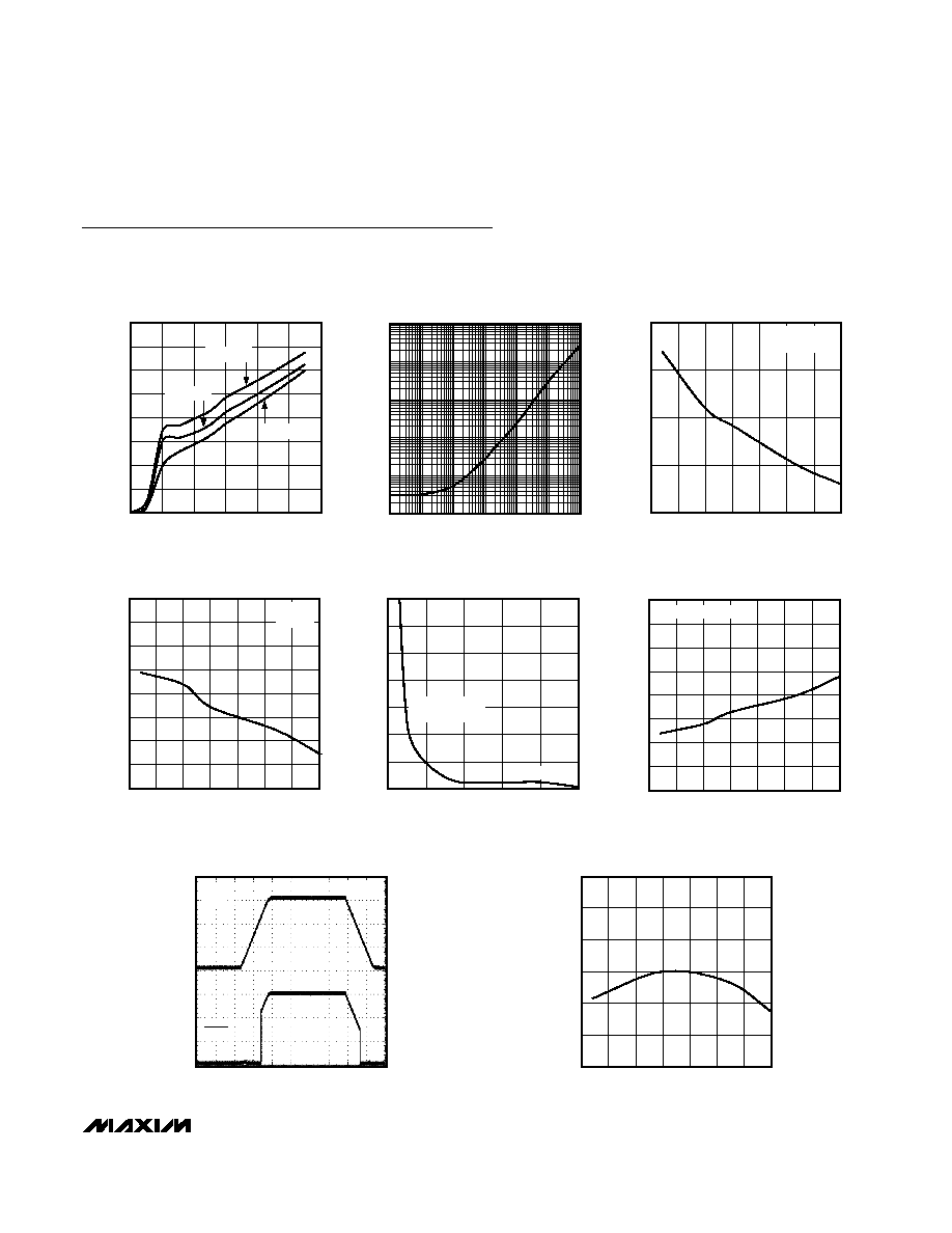
Typical Operating Characteristics
(V
CC
= 5V, C
SRT
= 1500pF, T
A
= +25∞C, unless otherwise noted.)
MAX6340/MAX6421≠MAX6426
Low-Power, SC70/SOT µP Reset Circuits with
Capacitor-Adjustable Reset Timeout Delay
4
_______________________________________________________________________________________
Detailed Description
Reset Output
The reset output is typically connected to the reset input
of a µP. A µP's reset input starts or restarts the µP in a
known state. The MAX6340/MAX6421≠MAX6426 µP
supervisory circuits provide the reset logic to prevent
code-execution errors during power-up, power-down,
and brownout conditions (see Typical Operating
Characteristics).
RESET changes from high to low whenever V
CC
drops
below the threshold voltage. Once V
CC
exceeds the
threshold voltage, RESET remains low for the capacitor-
adjustable reset timeout period.
The MAX6422 active-high RESET output is the inverse
logic of the active-low RESET output. All device outputs
are guaranteed valid for V
CC
> 1V.
The MAX6340/MAX6423/MAX6425/MAX6426 are open-
drain RESET outputs. Connect an external pullup resis-
tor to any supply from 0 to 5.5V. Select a resistor value
large enough to register a logic low when RESET is
asserted and small enough to register a logic high
while supplying all input current and leakage paths
connected to the RESET line. A 10k
to 100k pullup
is sufficient in most applications.
Selecting a Reset Capacitor
The reset timeout period is adjustable to accommodate
a variety of µP applications. Adjust the reset timeout
period (t
RP
) by connecting a capacitor (C
SRT
) between
SRT and ground. Calculate the reset timeout capacitor
as follows:
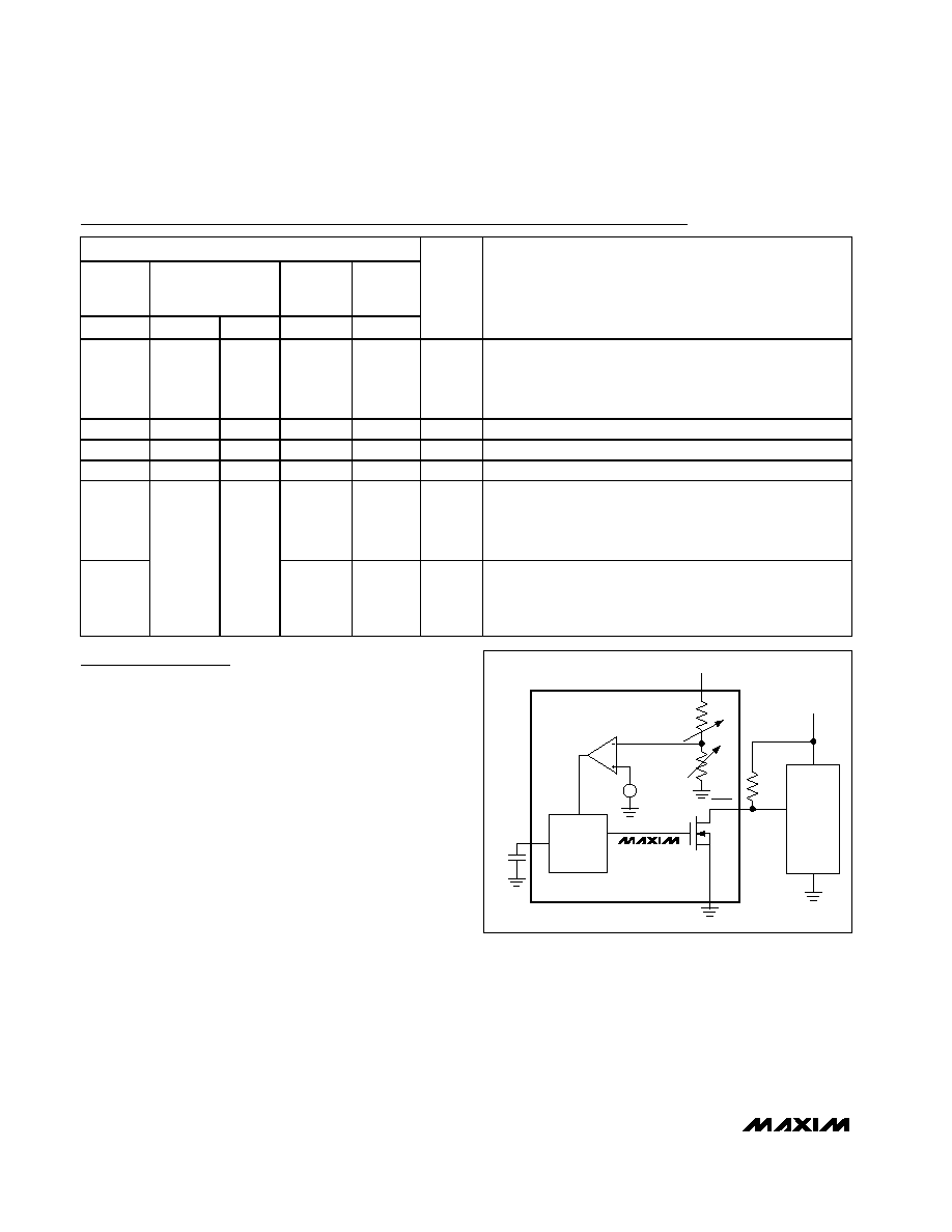
Pin Description
PIN
MAX6340
MAX6421
MAX6422
MAX6423
MAX6424
MAX6425
MAX6426
SOT23
SOT143
SC70
SOT23
SOT23
NAME
FUNCTION
1
3
3
5
1
SRT
Set Reset Timeout Input. Connect a capacitor between SRT
and ground to set the timeout period. Determine the period as
follows: t
RP
= 2.73
10
6
C
SRT
+ 275µs with t
RP
in seconds
and C
SRT
in farads.
2
1
2
3
2, 3
GND
Ground
3
--
--
4
--
N.C.
Not Internally Connected. Can be connected to GND.
4
2
1
2
5
V
CC
Supply Voltage and Reset Threshold Monitor Input
5
1
4
RESET
RESET changes from high to low whenever V
CC
drops below
the selected reset threshold voltage. RESET remains low for
the reset timeout period after V
CC
exceeds the reset
threshold.
--
4
4
--
--
RESET
RESET changes from low to high whenever V
CC
drops below
the selected reset threshold voltage. RESET remains high for
the reset timeout period after V
CC
exceeds the reset
threshold.
MAX6340
MAX6423
MAX6425
MAX6426
V
REF
C
SRT
SRT
RESET
TIMEOUT
N
GND
RESET
LASER-TRIMMED
RESISTORS
V
CC
3.3V
10k
5.0V
5V
SYSTEM
Figure 1. MAX6340/MAX6423/MAX6425/MAX6426 Open-Drain
RESET Output Allows Use with Multiple Supplies
MAX6340/MAX6421≠MAX6426
Low-Power, SC70/SOT µP Reset Circuits with
Capacitor-Adjustable Reset Timeout Delay
_______________________________________________________________________________________
5
C
SRT
= (t
RP
- 275µs) / (2.73
10
6
)
where t
RP
is in seconds and C
SRT
is in farads.
The reset delay time is set by a current/capacitor-con-
trolled ramp compared to an internal 0.65V reference.
An internal 240nA ramp current source charges the
external capacitor. The charge to the capacitor is
cleared when a reset condition is detected. Once the
reset condition is removed, the voltage on the capacitor
ramps according to the formula: dV/dt = I/C. The C
SRT
capacitor must ramp to 0.65V to deassert the reset.
C
SRT
must be a low-leakage (<10nA) type capacitor;
ceramic is recommended.
Operating as a Voltage Detector
The MAX6340/MAX6421≠MAX6426 can be operated in a
voltage detector mode by floating the SRT pin. The reset
delay times for V
CC
rising above or falling below the
threshold are not significantly different. The reset output is
deasserted smoothly without false pulses.
Applications Information
Interfacing to Other Voltages for Logic
Compatibility
The open-drain outputs of the MAX6340/MAX6423/
MAX6425/MAX6426 can be used to interface to µPs with
other logic levels. As shown in Figure 1, the open-drain
output can be connected to voltages from 0 to 5.5V. This
allows for easy logic compatibility to various µPs.
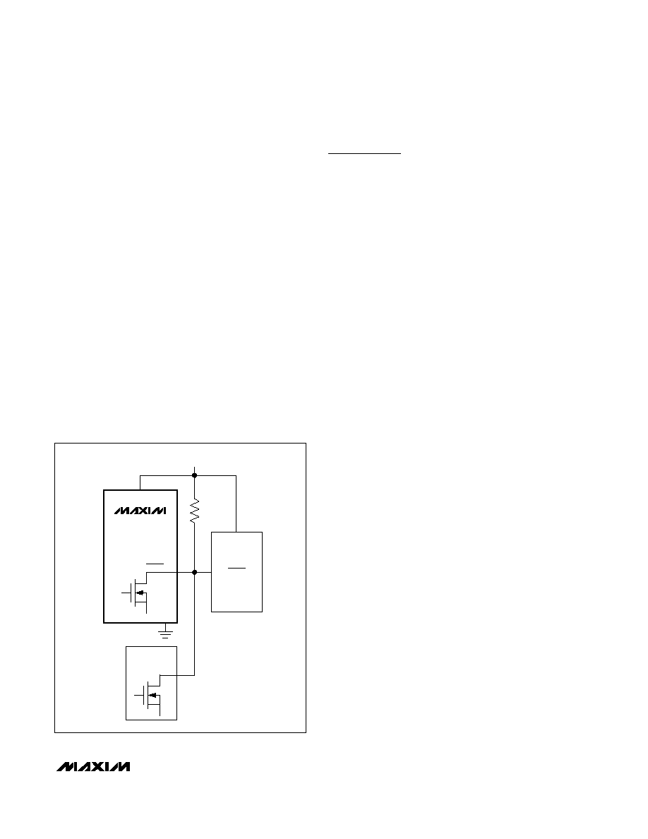
Wired-OR Reset
To allow auxiliary circuitry to hold the system in reset,
an external open-drain logic signal can be connected
to the open-drain RESET of the MAX6340/MAX6423/
MAX6425/MAX6426, as shown in Figure 2. This config-
uration can reset the µP, but does not provide the reset
timeout when the external logic signal is released.
Negative-Going V
CC
Transients
In addition to issuing a reset to the µP during power-up,
power-down, and brownout conditions, these supervisors
are relatively immune to short-duration negative-going
transients (glitches). The graph Maximum Transient
Duration vs. Reset Threshold Overdrive in the Typical
Operating Characteristics shows this relationship.
The area below the curve of the graph is the region in
which these devices typically do not generate a reset
pulse. This graph was generated using a negative-
going pulse applied to V
CC
, starting above the actual
reset threshold (V
TH
) and ending below it by the magni-
tude indicated (reset-threshold overdrive). As the mag-
nitude of the transient decreases (farther below the
reset threshold), the maximum allowable pulse width
decreases. Typically, a V
CC
transient that goes 100mV
below the reset threshold and lasts 50µs or less does
not cause a reset pulse to be issued.
Ensuring a Valid RESET or RESET
Down to V
CC
= 0
When V
CC
falls below 1V, RESET/RESET current-sink-
ing (sourcing) capabilities decline drastically. In the
case of the MAX6421/MAX6424, high-impedance
CMOS-logic inputs connected to RESET can drift to
undetermined voltages. This presents no problems in
most applications, since most µPs and other circuitry
do not operate with V
CC
below 1V.
In those applications where RESET must be valid down
to zero, adding a pulldown resistor between RESET
and ground sinks any stray leakage currents, holding
RESET low (Figure 3). The value of the pulldown resis-
tor is not critical; 100k
is large enough not to load
RESET and small enough to pull RESET to ground. For
applications using the MAX6422, a 100k
pullup resis-
V
DD
V
CC
MAX6340
MAX6423
MAX6425
MAX6426
RESET
N
N
GND
OPEN-DRAIN
LOGIC
µP
RESET
10k
Figure 2. Wired-OR Reset Circuit