 | ÐлекÑÑоннÑй компоненÑ: MAX6723A | СкаÑаÑÑ:  PDF PDF  ZIP ZIP |
MAX6715A-29A DS
General Description
The MAX6715AMAX6729A are ultra-low-voltage micro-
processor (µP) supervisory circuits designed to monitor two
or three system power-supply voltages. These devices
assert a system reset if any monitored supply falls below its
factory-trimmed or adjustable threshold and maintain reset
for a minimum timeout period after all supplies rise above
their thresholds. The integrated dual/triple supervisory cir-
cuits significantly improve system reliability and reduce size
compared to separate ICs or discrete components.
These devices monitor primary supply voltages (V
CC
1)
from 1.8V to 5.0V and secondary supply voltages (V
CC
2)
from 0.9V to 3.3V with factory-trimmed reset threshold
voltage options (see the Reset Voltage Threshold Suffix
Guide). An externally adjustable RSTIN input option
allows customers to monitor a third supply voltage down
to 0.62V. These devices are guaranteed to be in the cor-
rect reset output logic state when either V
CC
1 or V
CC
2
remains greater than 0.8V.
A variety of push-pull or open-drain reset outputs along
with watchdog input, manual reset input, and power-fail
input/output features are available (see the Selector
Guide). Select reset timeout periods from 1.1ms to
1120ms (min) (see the Reset Timeout Period Suffix
Guide). The MAX6715AMAX6729A are available in small
5-, 6-, and 8-pin SOT23 packages and operate over the
-40°C to +125°C temperature range.
Applications
Features
V
CC
1 (Primary Supply) Reset Threshold Voltages
from 1.58V to 4.63V
V
CC
2 (Secondary Supply) Reset Threshold
Voltages from 0.79V to 3.08V
Externally Adjustable RSTIN Threshold for
Auxiliary/Triple-Voltage Monitoring
(0.62V Internal Reference)
Watchdog Timer Option
35s (min) Long Startup Period
1.12s (min) Normal Timeout Period
Manual Reset Input Option
Power-Fail Input/Power-Fail Output Option
(Push-Pull and Open-Drain Active-Low)
Guaranteed Reset Valid Down to V
CC
1 or
V
CC
2 = 0.8V
Reset Output Logic Options
Immune to Short V
CC
Transients
Low Supply Current 14µA (typ) at 3.6V
Watchdog Disable Feature
Small 5-, 6-, and 8-Pin SOT23 Packages
MAX6715AMAX6729A
Dual/Triple, Ultra-Low-Voltage, SOT23 µP
Supervisory Circuits
________________________________________________________________ Maxim Integrated Products
1
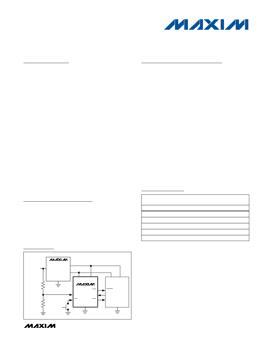
Ordering Information
IN
OUT2
OUT1
DC/DC
CONVERTER
UNREGULATED
DC
R1
R2
V
CC
1
V
CC
2
RSTIN/PFI
MR
RST
WDI
PFO
MAX67_ _
PUSHBUTTON
SWITCH
I/O
SUPPLY
CORE
SUPPLY
RESET
I/O
NMI
µP
1.8V
0.9V
MAX6715A-
MAX6729A
Typical Operating Circuit
19-0536; Rev 1; 7/06
For pricing, delivery, and ordering information, please contact Maxim/Dallas Direct! at
1-888-629-4642, or visit Maxim's website at www.maxim-ic.com.
Pin Configurations and Selector Guide appear at end of
data sheet.
PART
TEMP
RANGE
PIN-
PACKAGE
PKG
CODE
MAX6715AUT_ _D_+T
-40°C +125°C
6 SOT23-6
U6-1
MAX6716AUT_ _D_+T
-40°C +125°C
6 SOT23-6
U6-1
MAX6717AUK_ _D_+T
-40°C +125°C
5 SOT23-5
U5-1
MAX6718AUK_ _D_+T
-40°C +125°C
5 SOT23-5
U5-1
MAX6719AUT_ _D_+T
-40°C +125°C
6 SOT23-6
U6-1
MAX6720AUT_ _D_+T
-40°C +125°C
6 SOT23-6
U6-1
Note: The first "_ _" are placeholders for the threshold voltage
levels of the devices. Desired threshold levels are set by the part
number suffix found in the Reset Voltage Threshold Suffix Guide.
The "_" after the D is a placeholder for the reset timeout delay
time. Desired delay time is set using the timeout period suffix
found in the Reset Timeout Period Suffix Guide. For example, the
MAX6716AUTLTD3-T is a dual-voltage supervisor V
TH
1 =
4.625V, V
TH
2 = 3.075V, and 210ms (typ) timeout period.
Ordering Information continued at end of data sheet.
+Denotes lead-free package.
Multivoltage Systems
Telecom/Networking
Equipment
Computers/Servers
Portable/Battery-
Operated Equipment
Industrial Equipment
Printers/Fax Machines
Set-Top Boxes
MAX6715AMAX6729A
Dual/Triple, Ultra-Low-Voltage, SOT23 µP
Supervisory Circuits
2
_______________________________________________________________________________________
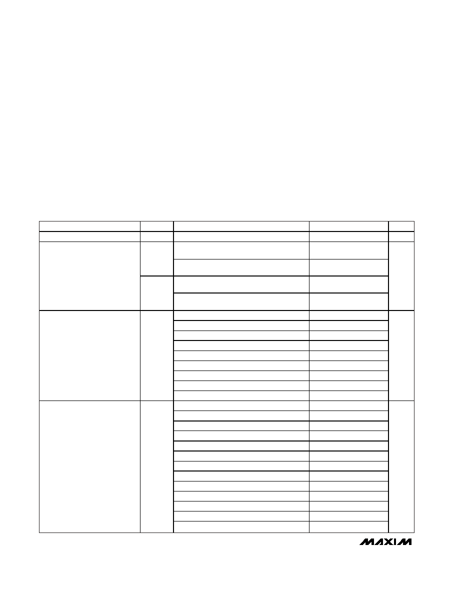
ABSOLUTE MAXIMUM RATINGS
ELECTRICAL CHARACTERISTICS
(V
CC
1 = V
CC
2 = 0.8V to 5.5V, GND = 0V, T
A
= -40°C to +125°C, unless otherwise noted. Typical values are at T
A
= +25°C.) (Note 1)
Stresses beyond those listed under "Absolute Maximum Ratings" may cause permanent damage to the device. These are stress ratings only, and functional
operation of the device at these or any other conditions beyond those indicated in the operational sections of the specifications is not implied. Exposure to
absolute maximum rating conditions for extended periods may affect device reliability.
Terminal Voltage (with respect to GND)
V
CC
1, V
CC
2 ..........................................................-0.3V to +6V
Open-Drain
RST, RST1, RST2, PFO, RST ................-0.3V to +6V
Push-Pull RST, RST1, PFO, RST...............-0.3V to (V
CC
1 + 0.3V)
Push-Pull RST2 .........................................-0.3V to (V
CC
2 + 0.3V)
RSTIN, PFI, MR, WDI ................................................-0.3V to +6V
Input Current/Output Current (all pins) ...............................20mA
Continuous Power Dissipation (T
A
= +70°C)
5-Pin SOT23-5 (derate 7.1mW/°C above +70°C) ........571mW
6-Pin SOT23-6 (derate 8.7mW/°C above +70°C) ........696mW
8-Pin SOT23-8 (derate 8.9mW/°C above +70°C) ........714mW
Operating Temperature Range .........................-40°C to +125°C
Storage Temperature Range .............................-65°C to +150°C
Junction Temperature ......................................................+150°C
Lead Temperature (soldering, 10s) .................................+300°C
PARAMETER
SYMBOL
CONDITIONS
MIN
TYP
MAX
UNITS
Supply Voltage
V
CC
0.8
5.5
V
V
CC
1 < 5.5V all I/O connections open,
outputs not asserted
15
39
I
CC1
V
CC
1 < 3.6V all I/O connections open,
outputs not asserted
10
28
V
CC
2 < 3.6V all I/O connections open,
outputs not asserted
4
11
Supply Current
I
CC2
V
CC
2 < 2.75V all I/O connections open,
outputs not asserted
3
9
µA
L (falling)
4.500
4.625
4.750
M (falling)
4.250
4.375
4.500
T (falling)
3.000
3.075
3.150
S (falling)
2.850
2.925
3.000
R (falling)
2.550
2.625
2.700
Z (falling)
2.250
2.313
2.375
Y (falling)
2.125
2.188
2.250
W (falling)
1.620
1.665
1.710
V
CC
1 Reset Threshold
V
TH1
V (falling)
1.530
1.575
1.620
V
T (falling)
3.000
3.075
3.150
S (falling)
2.850
2.925
3.000
R (falling)
2.550
2.625
2.700
Z (falling)
2.250
2.313
2.375
Y (falling)
2.125
2.188
2.250
W (falling)
1.620
1.665
1.710
V (falling)
1.530
1.575
1.620
I (falling)
1.350
1.388
1.425
H (falling)
1.275
1.313
1.350
G (falling)
1.080
1.110
1.140
F (falling)
1.020
1.050
1.080
E (falling)
0.810
0.833
0.855
V
CC
2 Reset Threshold
V
TH2
D (falling)
0.765
0.788
0.810
V
MAX6715AMAX6729A
Dual/Triple, Ultra-Low-Voltage, SOT23 µP
Supervisory Circuits
_______________________________________________________________________________________
3
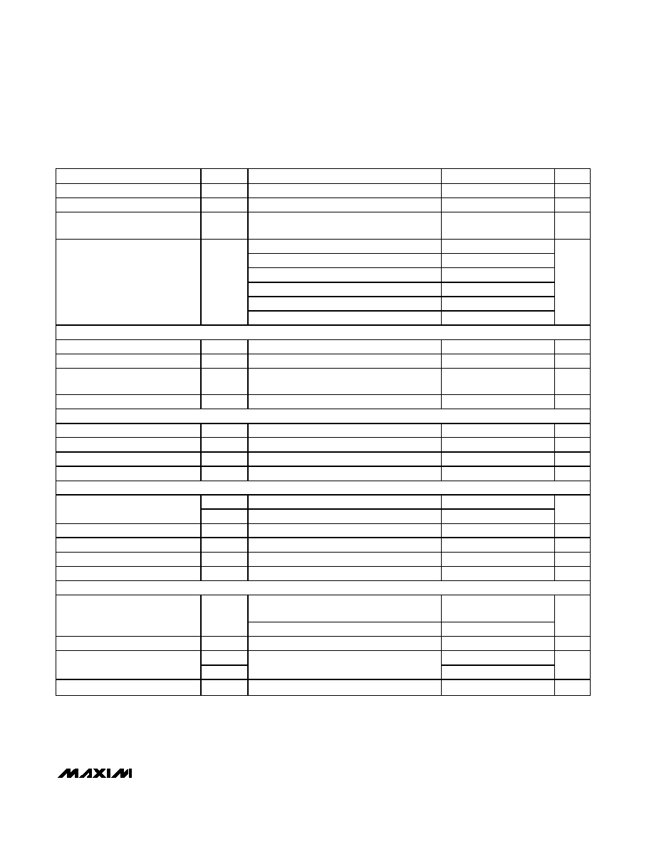
ELECTRICAL CHARACTERISTICS (continued)
(V
CC
1 = V
CC
2 = 0.8V to 5.5V, GND = 0V, T
A
= -40°C to +125°C, unless otherwise noted. Typical values are at T
A
= +25°C.) (Note 1)
PARAMETER
SYMBOL
CONDITIONS
MIN
TYP
MAX
UNITS
Reset Threshold Tempco
V
TH
/°C
20
ppm/°C
Reset Threshold Hysteresis
V
HYST
Referenced to V
TH
typical
0.5
%
V
CC
to Reset Output Delay
t
RD
V
C C
1 = ( V
TH
1
+ 100m V ) to ( V
TH
1 - 100m V ) or
V
C C
2 = ( V
TH
2 + 75m V ) to ( V
TH
2 - 75m V )
20
µs
D1
1.1
1.65
2.2
D2
8.8
13.2
17.6
D3
140
210
280
D5
280
420
560
D6
560
840
1120
Reset Timeout Period
t
RP
D4
1120
1680
2240
ms
ADJUSTABLE RESET COMPARATOR INPUT (MAX6719A/MAX6720A/MAX6723AMAX6727A)
RSTIN Input Threshold
V
RSTIN
611
626.5
642
mV
RSTIN Input Current
I
RSTIN
-100
+100
nA
RSTIN Hysteresis
3
mV
RSTIN to Reset Output Delay
t
RSTIND
V
RSTIN
to (V
RSTIN
- 30mV)
22
µs
POWER-FAIL INPUT (MAX6728A/MAX6729A)
PFI Input Threshold
V
PFI
611
626.5
642
mV
PFI Input Current
I
PFI
-100
+100
nA
PFI Hysteresis
V
PFH
3
mV
PFI to PFO Delay
t
DPF
(V
PFI
+ 30mV) to (V
PFI
- 30mV)
2
µs
MANUAL RESET INPUT (MAX6715AMAX6722A/MAX6725AMAX6729A)
V
IL
0.3
V
CC
1
MR Input Voltage
V
IH
0.7
V
CC
1
V
MR Minimum Pulse Width
1
µs
MR Glitch Rejection
100
ns
MR to Reset Delay
t
MR
200
ns
MR Pullup Resistance
25
50
80
k
WATCHDOG INPUT (MAX6721AMAX6729A)
First watchdog period after reset timeout
period
35
54
72
Watchdog Timeout Period
t
WD
Normal mode
1.12
1.68
2.24
s
WDI Pulse Width
t
WDI
(Note 2)
50
ns
V
IL
0.3
V
CC
1
WDI Input Voltage
V
IH
0.7
V
CC
1
V
WDI Input Current
I
WDI
WDI = 0V or V
CC
1
-1
+1
µA
MAX6715AMAX6729A
Dual/Triple, Ultra-Low-Voltage, SOT23 µP
Supervisory Circuits
4
_______________________________________________________________________________________
Note 1: Devices tested at +25°C. Overtemperature limits are guaranteed by design and not production tested.
Note 2: Parameter guaranteed by design.
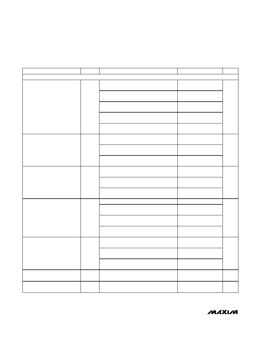
ELECTRICAL CHARACTERISTICS (continued)
(V
CC
1 = V
CC
2 = 0.8V to 5.5V, GND = 0V, T
A
= -40°C to +125°C, unless otherwise noted. Typical values are at T
A
= +25°C.) (Note 1)
PARAMETER
SYMBOL
CONDITIONS
MIN
TYP
MAX
UNITS
RESET/POWER-FAIL OUTPUTS
V
CC
1 or V
CC
2
0.8V, I
SINK
= 1µA,
output asserted
0.3
V
CC
1 or V
CC
2
1.0V, I
SINK
= 50µA,
output asserted
0.3
V
CC
1 or V
CC
2
1.2V, I
SINK
= 100µA,
output asserted
0.3
V
CC
1 or V
CC
2
2.7 V, I
SINK
= 1.2mA,
output asserted
0.3
RST/RST1/RST2/PFO
Output LOW
(Push-Pull or Open-Drain)
V
OL
V
CC
1 or V
CC
2
4.5V, I
SINK
= 3.2mA,
output asserted
0.4
V
V
CC
1
1.8V, I
SOURCE
= 200µA, output not
asserted
0.8
V
CC
1
V
CC
1
2.7V, I
SOURCE
= 500µA, output not
asserted
0.8
V
CC
1
RST/RST1/PFO
Output HIGH
(Push-Pull Only)
V
OH
V
CC
1
4.5V, I
SOURCE
= 800µA, output not
asserted
0.8
V
CC
1
V
V
CC
1
1.8V, I
SOURCE
= 200µA, output not
asserted
0.8
V
CC
2
V
CC
1
2.7V, I
SOURCE
= 500µA, output not
asserted
0.8
V
CC
2
RST2
Output HIGH
(Push-Pull Only)
V
OH
V
CC
1
4.5V, I
SOURCE
= 800µA, output not
asserted
0.8
V
CC
2
V
V
CC
1
1.0V, I
SOURCE
= 1µA, reset asserted
0.8
V
CC
1
V
CC
1
1.8V, I
SOURCE
= 150µA,
reset asserted
0.8
V
CC
1
V
CC
1
2.7V, I
SOURCE
= 500µA,
reset asserted
0.8
V
CC
1
RST
Output HIGH
(Push-Pull Only)
V
OH
V
CC
1
4.5V, I
SOURCE
= 800µA,
reset asserted
0.8
V
CC
1
V
V
CC
1 or V
CC
2
1.8V, I
SINK
= 500µA,
reset not asserted
0.3
V
CC
1 or V
CC
2
2.7V, I
SINK
= 1.2mA,
reset not asserted
0.3
RST
Output LOW
(Push-Pull or Open Drain)
V
OL
V
CC
1 or V
CC
2
4.5V, I
SINK
= 3.2mA,
reset not asserted
0.4
V
RST/RST1/RST2/PFO Output
Open-Drain Leakage Current
Output not asserted
0.5
µA
RST Output Open-Drain
Leakage Current
Output asserted
0.5
µA
MAX6715AMAX6729A
Dual/Triple, Ultra-Low-Voltage, SOT23 µP
Supervisory Circuits
_______________________________________________________________________________________
5
0
2
6
4
12
10
8
18
16
14
20
-40
20
-10
50
80
5
-25
35
65
110
95
125
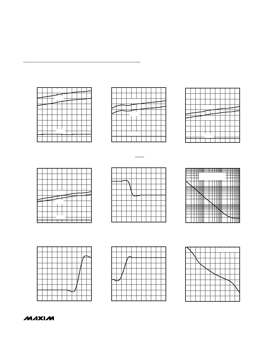
SUPPLY CURRENT vs. TEMPERATURE
(V
CC
1 = +5V, V
CC
2 = +3.3V)
MAX6715A-29A toc01
TEMPERATURE (
°C)
SUPPLY CURRENT (
µ
A)
TOTAL
I
CC
1
I
CC
2
0
4
2
10
8
6
18
16
14
12
20
SUPPLY CURRENT vs. TEMPERATURE
(V
CC
1 = +3.3V, V
CC
2 = +2.5V)
MAX6715A-29A toc02
TEMPERATURE (
°C)
SUPPLY CURRENT (
µ
A)
-40
20
-10
50
80
5
-25
35
65
110
95
125
TOTAL
I
CC
1
I
CC
2
0
2
6
4
12
10
8
18
16
14
20
-40
20
-10
50
80
5
-25
35
65
110
95
125
SUPPLY CURRENT vs. TEMPERATURE
(V
CC
1 = +2.5V, V
CC
2 = +1.8V)
MAX6715A-29A toc03
TEMPERATURE (
°C)
SUPPLY CURRENT (
µ
A)
TOTAL
I
CC
1
I
CC
2
0
2
6
4
12
10
8
18
16
14
20
-40
20
-10
50
80
5
-25
35
65
110
95
125
SUPPLY CURRENT vs. TEMPERATURE
(V
CC
1 = +1.8V, V
CC
2 = +1.2V)
MAX6715A-29A toc04
TEMPERATURE (
°C)
SUPPLY CURRENT (
µ
A)
TOTAL
I
CC
1
I
CC
2
0.980
0.984
0.992
0.988
1.004
1.000
0.996
1.016
1.012
1.008
1.020
-40
20
-10
50
80
5
-25
35
65
110
95
125
NORMALIZED/RESET WATCHDOG
TIMEOUT PERIOD vs. TEMPERATURE
MAX6715A-29A toc05
TEMPERATURE (
°C)
RESET/WATCHDOG TIMEOUT PERIOD
10,000
1000
100
10
1
100
10
1000
MAXIMUM V
CC
TRANSIENT DURATION
vs. RESET THRESHOLD OVERDRIVE
MAX6715A-29A toc06
RESET THRESHOLD OVERDRIVE (mV)
MAXIMUM V
CC
TRANSIENT DURATION (
µ
s)
RESET OCCURS ABOVE
THIS LINE
0.998
0.999
1.001
1.000
1.004
1.003
1.002
1.007
1.006
1.005
1.008
-40
20
-10
50
80
5
-25
35
65
110
95
125
NORMALIZED V
CC
RESET THRESHOLD
vs. TEMPERATURE
MAX6715A-29A toc07
TEMPERATURE (
°C)
RESET THRESHOLD
628
630
629
633
632
631
637
636
634
635
638
-40
20
-10
50
80
5
-25
35
65
110
95
125
RESET INPUT AND POWER-FAIL INPUT
THRESHOLD vs. TEMPERATURE
MAX6715A-29A toc08
TEMPERATURE (
°C)
RESET THRESHOLD
10
11
13
12
16
15
14
19
18
17
20
-40
20
-10
50
80
5
-25
35
65
110
95
125
V
CC
TO RESET DELAY
vs. TEMPERATURE
MAX6715A-29A toc09
TEMPERATURE (
°C)
V
CC
TO RESET DELAY (
µ
s)
75mV OVERDRIVE
Typical Operating Characteristics
(V
CC
1 = 5V, V
CC
2 = 3.3V, T
A
= +25°C, unless otherwise noted.)