
General Description
The MAX6821≠MAX6825 are low-voltage microprocessor
(µP) supervisory circuits that combine voltage monitor-
ing, watchdog timer, and manual reset input functions in
a 5-pin SOT23 package. Microprocessor supervisory cir-
cuits significantly improve system reliability and accura-
cy compared to separate ICs or discrete components.
These devices assert a reset signal whenever the moni-
tored voltage drops below its preset threshold, keeping it
asserted for a minimum timeout period after V
CC
rises
above the threshold. In addition, a watchdog timer moni-
tors against code execution errors. A debounced manual
reset is also available. The MAX6821≠MAX6825 monitor
voltages from +1.8V to +5.0V. These outputs are guaran-
teed to be in the correct state for V
CC
down to +1.0V.
Nine preprogrammed reset threshold voltages are
available (see Threshold Suffix Guide). The MAX6821,
MAX6822, and MAX6823 all have a manual reset input
and a watchdog timer. The MAX6821 has push-pull
RESET, the MAX6822 has open-drain RESET, and the
MAX6823 has push-pull RESET. The MAX6824 has a
watchdog timer and both push-pull RESET and push-
pull RESET. The MAX6825 has a manual reset input
and both push-pull RESET and push-pull RESET. The
Selector Guide explains the functions offered in this
series of parts.
________________________Applications
Features
o Monitors +1.8V, +2.5V, +3.0V, +3.3V, +5.0V
Supplies
o 140ms (min) Reset Timeout Delay
o 1.6s Watchdog Timeout Period
(MAX6821/MAX6822/MAX6823/MAX6824)
o Manual Reset Input
(MAX6821/MAX6822/MAX6823/MAX6825)
o Three Reset Output Options
Push-Pull RESET
Push-Pull RESET
Open-Drain RESET
o Guaranteed Reset Valid to V
CC
= +1.0V
o Immune to Short Negative V
CC
Transients
o No External Components
o Small 5-Pin SOT23 Packages
MAX6821≠MAX6825
Low-Voltage SOT23 µP Supervisors with
Manual Reset and Watchdog Timer
________________________________________________________________ Maxim Integrated Products
1
GND
WDI
MR
1
5
V
CC
RESET(RESET)
(RESET) MAX6821 ONLY
MAX6821
MAX6822
MAX6823
SOT23-5
TOP VIEW
2
3
4
Pin Configurations
19-1868; Rev 1; 1/01
Ordering Information
Threshold Suffix Guide
*Insert the desired suffix letter (from the table below) into the blank
to complete the part number.
Note: Bold indicates standard versions. Samples are typically
available for standard versions only. All parts require a 2.5k
minimum order increment. Contact factory for availability.
PART
*
TEMP. RANGE
PIN-PACKAGE
MAX6821_UK-T
-40
∞C to +125∞C
5 SOT23-5
MAX6822_UK-T
-40
∞C to +125∞C
5 SOT23-5
MAX6823_UK-T
-40
∞C to +125∞C
5 SOT23-5
MAX6824_UK-T
-40
∞C to +125∞C
5 SOT23-5
MAX6825_UK-T
-40
∞C to +125∞C
5 SOT23-5
SUFFIX
RESET
THRESHOLD (V)
L
4.63
M
4.38
T
3.08
S
2.93
R
2.63
Z
2.32
Y
2.19
W
1.67
V
1.58
Typical Operating Circuit appears at end of data sheet.
Pin Configurations continued at end of data sheet.
Selector Guide appears at end of data sheet.
Set-Top Boxes
Computers and
Controllers
Embedded Controllers
Intelligent Instruments
Automotive Systems
Critical µP Monitoring
Portable/Battery-
Powered Equipment
For price, delivery, and to place orders, please contact Maxim Distribution at 1-888-629-4642,
or visit Maxim's website at www.maxim-ic.com.

MAX6821≠MAX6825
Low-Voltage SOT23 µP Supervisors with
Manual Reset and Watchdog Timer
2
_______________________________________________________________________________________
ABSOLUTE MAXIMUM RATINGS
ELECTRICAL CHARACTERISTICS
(V
CC
= +4.5V to +5.5V for MAX682_L/M, V
CC
= +2.7V to +3.6V for MAX682_T/S/R, V
CC
= +2.1V to +2.75V for MAX682_Z/Y, V
CC
=
+1.53V to +2.0V for MAX682_W/V, T
A
= -40∞C to +125∞C, unless otherwise specified. Typical values are at T
A
= +25∞C.) (Note 1)
Stresses beyond those listed under "Absolute Maximum Ratings" may cause permanent damage to the device. These are stress ratings only, and functional
operation of the device at these or any other conditions beyond those indicated in the operational sections of the specifications is not implied. Exposure to
absolute maximum rating conditions for extended periods may affect device reliability.
V
CC
to GND ...........................................................-0.3V to +6.0V
Open-Drain RESET................................................-0.3V to +6.0V
Push-Pull RESET, RESET, MR, WDI ...........-0.3V to (V
CC
+ 0.3V)
Input Current (V
CC
) .............................................................20mA
Output Current (RESET, RESET).........................................20mA
Continuous Power Dissipation (T
A
= +70∞C)
5-Pin SOT23 (derate 7.1mW/∞C above +70∞C)............571mW
Operating Temperature Range .........................-40∞C to +125∞C
Junction Temperature ......................................................+150∞C
Storage Temperature Range .............................-65∞C to +150∞C
Lead Temperature (soldering, 10s) .................................+300∞C
PARAMETER
SYMBOL
CONDITIONS
MIN
TYP
MAX
UNITS
T
A
= 0
∞C to +85∞C
1.0
5.5
Operating Voltage Range
V
CC
T
A
= -40
∞C to +125∞C
1.2
5.5
V
T
A
= -40
∞C to +85∞C
10
20
V
CC
= +5.5V, no load
T
A
= -40
∞C to +125∞C
30
T
A
= -40
∞C to +85∞C
7
16
V
CC
= +3.6V, no load
T
A
= -40
∞C to +125∞C
25
T
A
= -40
∞C to +85∞C
5
12
V
CC
Supply Current
(MR and WDI Unconnected)
I
CC
V
CC
= +3.6V, no load
(MAX6825 only)
T
A
= -40
∞C to +125∞C
20
µA
T
A
= -40
∞C to +85∞C
4.50
4.63
4.75
MAX682_L
T
A
= -40
∞C to +125∞C
4.47
4.63
4.78
T
A
= -40
∞C to +85∞C
4.25
4.38
4.50
MAX682_M
T
A
= -40
∞C to +125∞C
4.22
4.38
4.53
T
A
= -40
∞C to +85∞C
3.00
3.08
3.15
MAX682_T
T
A
= -40
∞C to +125∞C
2.97
3.08
3.17
T
A
= -40
∞C to +85∞C
2.85
2.93
3.00
MAX682_S
T
A
= -40
∞C to +125∞C
2.83
2.93
3.02
T
A
= -40
∞C to +85∞C
2.55
2.63
2.70
MAX682_R
T
A
= -40
∞C to +125∞C
2.53
2.63
2.72
T
A
= -40
∞C to +85∞C
2.25
2.32
2.38
MAX682_Z
T
A
= -40
∞C to +125∞C
2.24
2.32
2.40
T
A
= -40
∞C to +85∞C
2.12
2.19
2.25
MAX682_Y
T
A
= -40
∞C to +125∞C
2.11
2.19
2.27
T
A
= -40
∞C to +85∞C
1.62
1.67
1.71
MAX682_W
T
A
= -40
∞C to +125∞C
1.61
1.67
1.72
V
CC
Reset Threshold
(V
CC
Falling)
V
TH
MAX682_V
T
A
= -40
∞C to +85∞C
1.52
1.58
1.62
V
Reset Threshold Temperature
Coefficient
60
p p m/∞C
Reset Threshold Hysteresis
2
V
TH
mV
V
CC
to Reset Output Delay
t
RD
V
CC
= V
TH
to (V
TH
- 100mV)
20
µs

MAX6821≠MAX6825
Low-Voltage SOT23 µP Supervisors with
Manual Reset and Watchdog Timer
_______________________________________________________________________________________
3
ELECTRICAL CHARACTERISTICS (continued)
(V
CC
= +4.5V to +5.5V for MAX682_L/M, V
CC
= +2.7V to +3.6V for MAX682_T/S/R, V
CC
= +2.1V to +2.75V for MAX682_Z/Y, V
CC
=
+1.53V to +2.0V for MAX682_W/V, T
A
= -40∞C to +125∞C, unless otherwise specified. Typical values are at T
A
= +25∞C.) (Note 1)
Note 1: Over-temperature limits are guaranteed by design and not production tested. Devices tested at T
A
= +25∞C.
Note 2: Guaranteed by design and not production tested.
PARAMETER
SYMBOL
CONDITIONS
MIN
TYP
MAX
UNITS
T
A
= -40
∞C to +85∞C
140
200
280
Reset Timeout Period
t
RP
T
A
= -40
∞C to +125∞C
100
320
ms
V
CC
1.0V, I
SINK
= 50µA, reset asserted,
T
A
= 0
∞C to
+85
∞C
0.3
V
CC
1.2V, I
SINK
= 100µA, reset asserted
0.3
V
CC
2.55V, I
SINK
= 1.2mA, reset asserted
0.3
RESET Output LOW
(Push-Pull or Open-Drain)
V
OL
V
CC
4.25V, I
SINK
= 3.2mA, reset asserted
0.4
V
V
CC
1.8V, I
SOURCE
= 200µA, reset not
asserted
0.8
V
CC
V
CC
3.15V, I
SOURCE
= 500µA, reset not
asserted
0.8
V
CC
RESET Output HIGH
(Push-Pull Only)
V
OH
V
CC
4.75V, I
SOURCE
= 800µA, reset not
asserted
0.8
V
CC
V
Open-Drain RESET Output
Leakage Current (Note 1)
I
LKG
V
CC
> V
TH
, RESET not asserted
1.0
µA
V
CC
1.0V, I
SOURCE
= 1µA, reset asserted,
T
A
= 0
∞C to
+85
∞C
0.8
V
CC
V
C C
1.50V , I
SOURCE
= 100µA, r eset asser ted 0.8
V C C
V
CC
2.55V , I
SOURCE
= 500µA, r eset asser ted 0.8
V C C
RESET Output HIGH
(Push-Pull Only)
V
OH
V
CC
4.25V , I
SOURCE
= 800µA, r eset asser ted 0.8
V C C
V
V
CC
1.8V , I
SINK
= 500µA, r eset not asser ted 0.3
V
CC
3.15V , I
SINK
= 1.2m A, r eset not asser ted 0.3
RE S E T Outp ut LO W
( P ush- P ul l Onl y)
V OL
V
CC
4.75V , I
S IN K
= 3.2m A, r eset not asser ted 0.4
V
MANUAL RESET INPUT (MAX6821/MAX6822/MAX6823/MAX6825)
V
IL
0.3
V
CC
MR Input Voltage
V
IH
0.7
V
CC
V
MR Minimum Input Pulse
1
µs
MR Glitch Rejection
100
ns
MR to Reset Delay
200
ns
MR Pullup Resistance
25
50
75
k
WATCHDOG INPUT (MAX6821/MAX6822/MAX6823/MAX6824)
T
A
= -40
∞C to
+85
∞C
1.12
1.60
2.40
Watchdog Timeout Period
t
WD
T
A
= -40
∞C to
+125
∞C
0.80
2.60
s
WDI Pulse Width (Note 2)
t
WDI
50
ns
V
IL
0.3
V
CC
WDI Input Voltage
V
IH
0.7
V
CC
V
WDI = V
CC
, time average
120
160
WDI Input Current
I
WDI
WDI = 0, time average
-20
-15
µA
MAX6821≠MAX6825
Low-Voltage SOT23 µP Supervisors with
Manual Reset and Watchdog Timer
4
_______________________________________________________________________________________
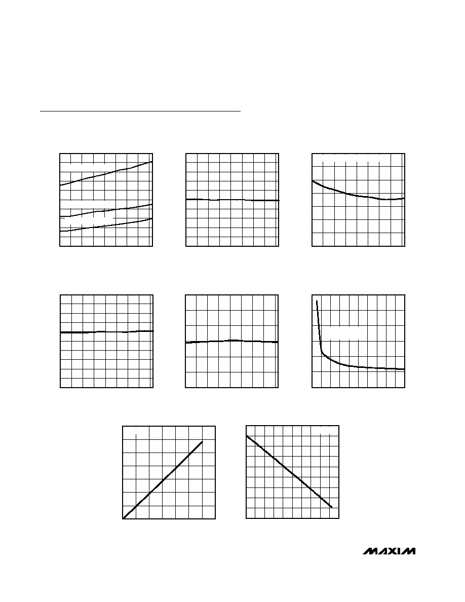
Typical Operating Characteristics
(T
A
= +25∞C, unless otherwise noted.)
3
5
4
7
6
9
8
10
12
11
13
-40
0
20
40
-20
60
80
100 120
SUPPLY CURRENT vs.
TEMPERATURE
MAX6821 toc01
TEMPERATURE (
∞C)
SUPPLY CURRENT (
µ
A)
V
CC
= +5V, L VERSION
V
CC
= +3.3V, S VERSION
V
CC
= +1.8V, V VERSION
150
170
160
190
180
210
200
220
240
230
250
-40
0
20
40
-20
60
80
100 120
RESET TIMEOUT PERIOD vs.
TEMPERATURE
MAX6821 toc02
TEMPERATURE (
∞C)
RESET TIMEOUT PERIOD (ms)
0
10
5
20
15
30
25
35
-40
0
20
-20
40
60
80
100 120
V
CC
TO RESET OUTPUT DELAY vs.
TEMPERATURE
MAX6821 toc03
TEMPERATURE (
∞C)
PROPAGATION DELAY (
µ
s)
V
CC
FALLING, V
CC
=
V
TH
-
100mV
1.0
1.2
1.1
1.4
1.3
1.6
1.5
1.7
1.9
1.8
2.0
-40
0
20
40
-20
60
80
100 120
WATCHDOG TIMEOUT PERIOD vs.
TEMPERATURE
MAX6821 toc04
TEMPERATURE (
∞C)
WATCHDOG TIMEOUT PERIOD (s)
0.94
0.96
1.00
0.98
1.04
1.02
1.06
-40
0
20
-20
40
60
80
100 120
NORMALIZED RESET THRESHOLD
DELAY vs. TEMPERATURE
MAX6821 toc05
TEMPERATURE (
∞C)
RESET THRESHOLD (V)
0
60
40
20
80
100
120
0
80
60
20 40
100 120 140 160 180 200
MAXIMUM V
CC
TRANSIENT DURATION
vs. RESET THRESHOLD OVERDRIVE
MAX6821 toc06
RESET THRESHOLD OVERDRIVE (mV), V
TH
- V
CC
TRANSIENT DURATION (
µ
s)
RESET OCCURS
ABOVE CURVE
0
0.10
0.05
0.20
0.15
0.30
0.25
0.35
0
2
3
1
4
5
6
7
VOLTAGE OUTPUT LOW vs. I
SINK
MAX6821 toc07
I
SINK
(mA)
V
OUT
(V)
V
CC
= +2.9V
2.74
2.78
2.76
2.82
2.80
2.84
2.86
2.90
2.88
2.92
0 0.1 0.2 0.3 0.4 0.5 0.6 0.7 0.8 0.9 1.0
VOLTAGE OUTPUT HIGH vs. I
SOURCE
MAX6821 toc08
I
SOURCE
(mA)
V
OUT
(V)
V
CC
= +2.9V

MAX6821≠MAX6825
Low-Voltage SOT23 µP Supervisors with
Manual Reset and Watchdog Timer
_______________________________________________________________________________________
5
Pin Description
PIN NUMBERS
MAX6821
MAX6822
MAX6823
MAX6824
MAX6825
PIN
NAME
FUNCTION
1
1
1
1
RESET
Active-Low Open-Drain or Push-Pull Reset Output. RESET
changes from high to low when the V
CC
input drops below the
selected reset threshold, MR is pulled low, or the watchdog
triggers a reset. RESET remains low for the reset timeout period
after V
CC
exceeds the device reset threshold, MR goes low to
high, or the watchdog triggers a reset.
1
3
3
RESET
Active-High Push-Pull Reset Output. RESET changes from low to
high when the V
CC
input drops below the selected reset threshold,
MR is pulled low, or the watchdog triggers a reset. RESET remains
high for the reset timeout period after V
CC
exceeds the device
reset threshold, MR goes low to high, or the watchdog triggers a
reset.
2
2
2
2
2
GND
Ground
3
3
3
4
MR
Active-Low Manual Reset Input. Internal 50k
pullup to V
CC
. Pull
low to force a reset. Reset remains active as long as MR is low
and for the reset timeout period after MR goes high. Leave
unconnected or connect to V
CC
if unused.
4
4
4
4
WDI
Watchdog Input. If WDI remains high or low for longer than the
watchdog timeout period, the internal watchdog timer runs out and
a reset is triggered for the reset timeout period. The internal
watchdog timer clears whenever reset is asserted, the manual
reset is asserted, or WDI sees a rising or falling edge. If WDI is
left unconnected or is connected to a three-stated buffer output,
the watchdog feature is disabled.
5
5
5
5
5
V
CC
Supply Voltage and Input for Reset Threshold Monitor
Detailed Description
RESET/RESET Output
A µP's reset input starts the µP in a known state. The
MAX6821≠MAX6825 µP supervisory circuits assert a
reset to prevent code-execution errors during power-
up, power-down, and brownout conditions. Whenever
V
CC
falls below the reset threshold, the reset output
asserts low for RESET and high for RESET. Once V
CC
exceeds the reset threshold, an internal timer keeps the
reset output asserted for the specified reset timeout
period (t
RP
); after this interval, reset output returns to its
original state (see Figure 2).
Manual Reset Input
Many µP-based products require manual reset capabil-
ity, allowing the operator, a test technician, or external
logic circuitry to initiate a reset. On the MAX6821/
MAX6822/MAX6823/MAX6825, a logic low on MR
asserts a reset. Reset remains asserted while MR is
low, and for the timeout period (140ms min) after it
returns high. MR has an internal 50k
pullup resistor,
so it can be left open if not used. This input can be dri-
ven with CMOS logic levels or with open-drain/collector
outputs. Connect a normally open momentary switch
from MR to GND to create a manual reset function;
external debounce circuitry is not required. If MR is dri-
ven from long cables or the device is used in a noisy
environment, connect a 0.1µF capacitor from MR to
GND to provide additional noise immunity.
Watchdog Input
In the MAX6821≠MAX6824, the watchdog circuit moni-
tors the µP's activity. If the µP does not toggle (low to
high or high to low) the watchdog input (WDI) within the
watchdog timeout period (1.6s nominal), reset asserts
for the reset timoeout period. The internal 1.6s timer
can be cleared by either a reset pulse or by toggling
WDI. The WDI can detect pulses as short as 50ns.
While reset is asserted, the timer remains cleared and
does not count. As soon as reset is released, the timer
starts counting (see Figure 3).