Äîêóìåíòàöèÿ è îïèñàíèÿ www.docs.chipfind.ru
General Description
The MAX6950/MAX6951 are compact common-cath-
ode display drivers that interface microprocessors to
individual 7-segment numeric LED digits, bar graph, or
discrete LEDs through an SPITM-, QSPITM-MICROWIRETM-
compatible serial interface. The supply voltage can be
as low as 2.7V.
The MAX6950 drives up to five 7-segment digits or 40
discrete LEDs. The MAX6951 drives up to eight 7-seg-
ment digits or 64 discrete LEDs.
Included on-chip are hexadecimal character decoders
(09, AF), multiplex scan circuitry, segment and digit
drivers, and a static RAM that stores each digit. The
user may select hexadecimal decoding or no-decode
for each digit to allow any mix of 7-segment digits, bar
graph, or discrete LEDs to be driven. The segment cur-
rent for the LEDs is set by an internal digital brightness
control. The segment drivers are slew-rate limited to
reduce EMI.
Individual digits may be addressed and updated with-
out rewriting the entire display. The devices include a
low-power shutdown mode, digital brightness control, a
scan-limit register that allows the user to display from
one to eight digits, segment blinking that can be syn-
chronized across drivers, and a test mode that forces
all LEDs on.
Applications
Set-Top Boxes
Panel Meters
White Goods
Bar Graphs and Matrix Displays
Industrial Controllers and Instrumentation
Professional Audio Equipment
Medical Equipment
Features
o
High-speed 26MHz SPI-, QSPI-, MICROWIRE-
Compatible Serial Interface
o
+2.7V to +5.5V Operation
o
Individual LED Segment Control
o
Segment Blinking Control that Can Be
Synchronized Across Multiple Drivers
o
Hexadecimal Decode/No-Decode Digit Selection
o
Digital Brightness Control
o
Display Blanked on Power-Up
o
Drives Common-Cathode LED Digits
o
Multiplex Clock Syncronizable to External Clock
o
Slew-Rate Limited Segment Drivers for Low EMI
o
75µA Low-Power Shutdown (Data Retained)
o
Small 16-Pin QSOP Package
MAX6950/MAX6951
Serially Interfaced, +2.7V to +5.5V,
5- and 8-Digit LED Display Drivers
________________________________________________________________ Maxim Integrated Products
1
16
15
14
13
12
11
10
9
1
2
3
4
5
6
7
8
DIN
V+
(DIG6)/SEG6
DIG4/SEG4
(DIG5)/SEG5
(DIG7)/SEG7
SEG8
OSC
TOP VIEW
MAX6950
MAX6951
QSOP
CS
CLK
DIG3/SEG3
DIG0/SEG0
DIG2/SEG2
DIG1/SEG1
ISET
GND
( ) MAX6951 ONLY
Pin Configuration
19-2227; Rev 1; 12/01
For pricing, delivery, and ordering information, please contact Maxim/Dallas Direct! at
1-888-629-4642, or visit Maxim's website at www.maxim-ic.com.
Ordering Information
PART
TEMP. RANGE
PIN-PACKAGE
MAX6950
CEE
0°C to +70°C
16 QSOP
MAX6950EEE
-40°C to +85°C
16 QSOP
MAX6951
CEE
0°C to +70°C
16 QSOP
MAX6951EEE
-40°C to +85°C
16 QSOP
Functional Diagram appears at end of data sheet.
Typical Application appears at end of data sheet.
SPI and QSPI are trademarks of Motorola, Inc.
MICROWIRE is a trademark of National Semiconductor Corp.
MAX6950/MAX6951
Serially Interfaced, +2.7V to +5.5V,
5- and 8-Digit LED Display Drivers
2
_______________________________________________________________________________________
ABSOLUTE MAXIMUM RATINGS
Stresses beyond those listed under "Absolute Maximum Ratings" may cause permanent damage to the device. These are stress ratings only, and functional
operation of the device at these or any other conditions beyond those indicated in the operational sections of the specifications is not implied. Exposure to
absolute maximum rating conditions for extended periods may affect device reliability.
Voltage (with Respect to GND)
V+..................................... ...................................-0.3V to 6V
All Other Pins................................................-0.3V to (V+ + 0.3V)
DIG1DIG8 Sink Current.................................................. 440mA
SEG1SEG9 Source Current.............................................. 55mA
Continuous Power Dissipation (T
A
= +70°C)
16-Pin QSOP (derate 8.34mW/°C above +70°C)........667mW
Operating Temperature Ranges (T
MIN
to T
MAX
)
MAX695_CEE....................................................0°C to +70°C
MAX695_EEE .................................................-40°C to +85°C
Junction Temperature ......................................................+150°C
Storage Temperature Range .............................-65°C to +150°C
Lead Temperature (soldering, 10s) .................................+300°C
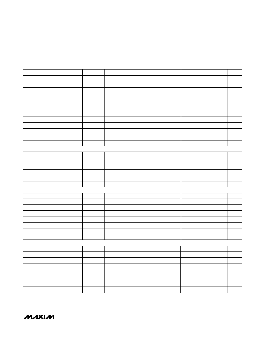
ELECTRICAL CHARACTERISTICS
(Typical operating circuit, V+ = +3.0V to +5.5V, T
A
= T
MIN
to T
MAX
, unless otherwise noted.) (Note 1)
PARAMETER
SYMBOL
CONDITIONS
MIN
TYP
MAX
UNITS
Operating Supply Voltage
V+
2.7
5.5
V
Overtemperature
75
Shutdown Supply Current
I
SHDN
S hutd ow n m od e, al l d i g i tal
i np uts at V + or GN D
T
A
= +25
o
C
62
160
µA
Operating Supply Current
I+
All segments on, all digits scanned,
intensity set to full, internal oscillator,
no display load connected
10
15
mA
OSC = RC oscillator
1
8
Master Clock Frequency (OSC
Internal Oscillator)
f
OSC
OSC = RC oscillator, R
SET
= 56k
,
C
SET
= 27pF
4
MHz
Master Clock Frequency (OSC
External Clock)
f
OSC
OSC overdriven externally
1
8
MHz
Display Scan Rate (OSC
External Clock)
f
SCAN
Eight digits scanned, OSC = overdriven
externally
155
1250
Hz
Display Scan Rate (OSC Internal
Oscillator)
f
SCAN
Eight digits scanned, OSC = RC oscillator
155
1250
Hz
Display Scan Rate (OSC Internal
Oscillator)
f
SCAN
Eight digits scanned, OSC = RC oscillator,
R
SET
= 56k
, C
SET
= 27pF
625
Hz
OSC Internal/External Detection
Threshold
V
OSC
1.7
V
Dead Clock Protection
Frequency
f
OSC
75.5
kHz
OSC High Time (OSC External
Clock)
t
CH
50
ns
OSC Low Time (OSC External
Clock)
t
CL
50
ns
MAX6950/MAX6951
Serially Interfaced, +2.7V to +5.5V,
5- and 8-Digit LED Display Drivers
_______________________________________________________________________________________
3
ELECTRICAL CHARACTERISTICS
(Typical operating circuit, V+ = +3.0V to +5.5V, T
A
= T
MIN
to T
MAX
, unless otherwise noted.) (Note 1)
PARAMETER
SYMBOL
CONDITIONS
MIN
TYP
MAX
UNITS
Slow Segment Blink Period
(Internal Oscillator)
f
S LOWBLIN K
Eight digits scanned, OSC = RC oscillator,
R
SET
= 56k
, C
SET
= 27pF
1
s
Fast Segment Blink Period
(Internal Oscillator)
f
FASTBLIN K
Eight digits scanned, OSC = RC oscillator,
R
SET
= 56k
, C
SET
= 27pF
0.5
s
Fast or Slow Segment Blink Duty
Cycle (Note 2)
49.9
50
50.1
%
Digit Drive Sink Current
I
DIGIT
T
A
= +25°C, V
LED
= 2.4V
240
320
400
mA
Segment Drive Source Current
I
SEG
T
A
= +25°C, V
LED
= 2.4V
-30
-40
-50
mA
Digit Drive Sink Current (Note 2)
I
DIGIT
T
A
= +25°C, V+ = 2.7V to 3V, V
LED
= 2.2V
80
mA
Segment Drive Source Current
(Note 2)
I
SEG
T
A
= +25°C, V+ = 2.7V to 3V, V
LED
= 2.2V
-10
mA
Slew Rate Rise Time
I
SEG
/
t
T
A
= +25°C
35
mA/µs
LOGIC INPUTS
Input Current DIN, CLK,
CS
I
IH
, I
IL
V
IN
= 0 or V+
-2
2
µA
Logic High Input Voltage DIN,
CLK,
CS
V
IH
2.4
V
Logic Low Input Voltage DIN,
CLK,
CS
V
IL
0.4
V
H yster esi s V ol tag e D IN , C LK,
C S
V
I
0.5
V
TIMING CHARACTERISTICS
(Figure 1)
CLK Clock Period
t
CP
38.4
ns
CLK Pulse Width High
t
CH
19
ns
CLK Pulse Width Low
t
CL
19
ns
C S Fall to CLK Ri se S etup Ti m e
t
CSS
9.5
ns
CLK Ri se to
CS Rise Hold Time
t
CSH
3
ns
DIN Setup Time
t
DS
9.5
ns
DIN Hold Time
t
DH
0
ns
CS Pulse High
t
CSW
19
ns
TIMING CHARACTERISTICS (V+ = +2.7V)
(Note 2)
CLK Clock Period
t
CP
50
ns
CLK Pulse Width High
t
CH
24
ns
CLK Pulse Width Low
t
CL
24
ns
C S Fall to CLK Ri se Setup Time
t
CSS
12
ns
CLK Ri se to
CS Rise Hold Time
t
CSH
4
ns
DIN Setup Time
t
DS
12
ns
DIN Hold Time
t
DH
4
ns
CS Pulse High
t
CSW
24
ns
Note 1:
All parameters tested at T
A
= +25°C. Specifications over temperature are guaranteed by design.
Note 2:
Guaranteed by design.
MAX6950/MAX6951
Serially Interfaced, +2.7V to +5.5V,
5- and 8-Digit LED Display Drivers
4
_______________________________________________________________________________________
INTERNAL OSCILLATOR FREQUENCY
vs. TEMPERATURE
MAX6950/1 toc01
3.60
3.70
3.90
3.80
4.20
4.30
4.10
4.00
4.40
OSCILLATOR FREQUENCY (MHz)
-40
0
20
-20
40
60
80
TEMPERATURE (
°
C)
V+ = 2.7V
V+ = 3.3V
V+ = 5V
3.60
3.70
3.80
3.90
4.00
4.10
4.20
4.30
4.40
2
3
4
5
6
INTERNAL OSCILLATOR FREQUENCY
vs. SUPPLY VOLTAGE
MAX6950/1 toc02
SUPPLY VOLTAGE (V)
OSCILLATOR FREQUENCY (MHz)
0
1.0
0.5
2.0
1.5
3.0
2.5
0
400
200
600
800
INTERNAL OSCILLATOR WAVEFORM
AT OSC (PIN 9)
MAX6950/1 toc03
TIMELINE (ns)
VOLTAGE AT OSC (V)
70
72
71
74
73
76
75
77
79
78
80
2.0
3.0
3.5
2.5
4.0
4.5
5.0
5.5
6.0
DEAD CLOCK OSCILLATOR FREQUENCY
vs. SUPPLY VOLTAGE
MAX6950/1 toc04
SUPPLY VOLTAGE (V)
OSCILLATOR FREQUENCY (kHz)
0.95
0.96
0.97
0.98
0.99
1.00
1.01
2.0
3.0
2.5
3.5
4.0
4.5
5.0
5.5
6.0
SEGMENT SOURCE CURRENT
vs. SUPPLY VOLTAGE
MAX6950/1 toc05
SUPPLY VOLTAGE (V)
CURRENT NORMALIZED TO 40mA
0
1.0
0.5
2.0
1.5
3.0
2.5
3.5
WAVEFORM AT SEGO/DIGO (PIN 6)
V+ = 3.3V, 8 DIGITS SCANNED, 8/16 INTENSITY
MAX6950/1 toc06
TIMELINE (ns)
VOLTAGE (V)
0
500
1000
1500
2000
DIGIT 0 MULTIPLEX TIMESLOT
Typical Operating Characteristics
(Typical operating circuit, scan limit set to eight digits, V+ = +3.3V, V
LED
= 2.4V, T
A
= +25°C, unless otherwise noted.)
Detailed Description
Differences Between
MAX6950 and MAX6951
The MAX6950 is a five-digit common-cathode display
driver. It drives five digits, with each digit comprising
eight LEDs with cathodes connected to a common
cathode. The display limit is therefore 40 LEDs or digit
segments.
The MAX6951 is an eight-digit common-cathode dis-
play driver. It drives eight digits, with each digit com-
prising eight LEDs. The only difference between the
MAX6950 and MAX6951 is that the MAX6950 is missing
three digit drivers. The MAX6950 can be configured to
scan eight digits, but if the last three digits are wired
up, they do not light.
The MAX6950/MAX6951 use a unique multiplexing
scheme to minimize the connections between the driver
and LED display. The scheme requires that the seg-
ment connections are different to each of the five
(MAX6950) or eight (MAX6951) digits (Table 1). This is
shown in the Typical Application Circuit, which uses
single-digit type displays. The MAX6950/MAX6951 are
not intended to drive multidigit display types, which
have the segments internally wired together, unless the
segments are wired with the common cathodes to fol-
low Table 1. The MAX6950/MAX6951 can drive multi-
digit LED displays that have the segments individually
pinned for each digit because then the digits can be
connected together correctly externally, just as if indi-
vidual digits were used.
Serial-Addressing Modes
The microprocessor interface on the MAX6950/
MAX6951 is a SPI-compatible 3-wire serial interface
using three input pins (Figure 1). This interface is used
to write configuration and display data to the MAX6950/
MAX6951. The serial interface data word length is 16
bits, which are labeled D15D0 (Table 2). D15D8 con-
tain the command address, and D7D0 contain the
data. The first bit received is D15, the most-significant
bit (MSB). The three input pins are:
·
CLK is the serial clock input, and may idle low or
high at the start and end of a write sequence.
·
CS is the MAX6950/MAX6951s' chip-select input,
and must be low to clock data into the MAX6950/
MAX6951.
·
DIN is the serial data input, and must be stable
when it is sampled on the rising edge of the clock.
The serial interface comprises a 16-bit shift register into
which DIN data is clocked on the rising edge of CLK
when
CS is low. When CS is high, transitions on CLK do
not clock data into the shift register. When
CS goes
MAX6950/MAX6951
Serially Interfaced, +2.7V to +5.5V,
5- and 8-Digit LED Display Drivers
_______________________________________________________________________________________
5
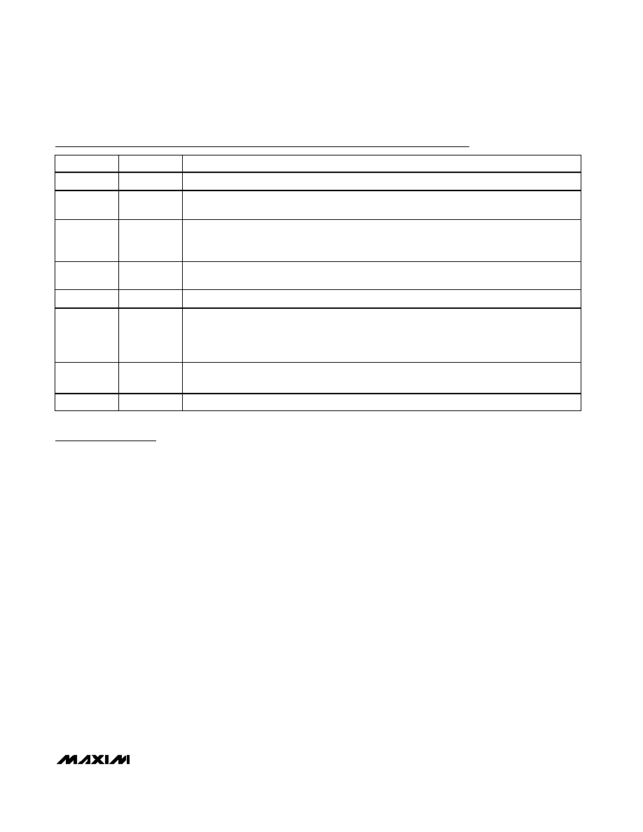
PIN
NAME
FUNCTION
1
DIN
Serial Data Input. Data is loaded into the internal 16bit Shift register on CLK's rising edge.
2
CLK
Serial-Clock Input. On CLK's rising edge, data is shifted into the Internal Shift register. On CLK's
falling edge, data is clocked out of DOUT. CLK input is active only while
CS is low.
36, 1014
DIGX, SEGX
Digit X outputs sink current from the display common cathode when acting as digit drivers.
Segment X drivers source current to the display. Segment/digit drivers are high impedance when
turned off.
7
I
SET
Current Setting. Connect to GND through a resistor (R
SET
) to set the peak current. This resistor,
together with capacitor C
SET
, also sets the multiplex clock frequency.
8
GND
Ground
9
OSC
Multiplexer Clock Input. A capacitor (C
SET
) is connected to GND when the internal RC oscillator
multiplex clock is used. Resistor R
SET
(also used to set the peak current) and capacitor C
SET
together set the multiplex clock frequency. When the external clock is used, OSC should be driven
by a 1MHz to 8MHz clock.
15
CS
Chip-Select Input. Serial data is loaded into the Shift register while
CS is low. The last 16 bits of
serial data are latched on
CS's rising edge.
16
V+
Positive Supply Voltage. Bypass to GND with a 0.1µF capacitor.
Pin Description