________________General Description
The MAX811/MAX812 are low-power microprocessor
(µP) supervisory circuits used to monitor power sup-
plies in µP and digital systems. They provide excellent
circuit reliability and low cost by eliminating external
components and adjustments when used with 5V-
powered or 3V-powered circuits. The MAX811/MAX812
also provide a debounced manual reset input.
These devices perform a single function: They assert a
reset signal whenever the V
CC
supply voltage falls
below a preset threshold, keeping it asserted for at
least 140ms after V
CC
has risen above the reset thresh-
old. The only difference between the two devices is that
the MAX811 has an active-low RESET output (which is
guaranteed to be in the correct state for V
CC
down to
1V), while the MAX812 has an active-high RESET out-
put. The reset comparator is designed to ignore fast
transients on V
CC
. Reset thresholds are available for
operation with a variety of supply voltages.
Low supply current makes the MAX811/MAX812 ideal
for use in portable equipment. The devices come in a
4-pin SOT143 package.
________________________Applications
Computers
Controllers
Intelligent Instruments
Critical µP and µC Power Monitoring
Portable/Battery-Powered Equipment
____________________________Features
o Precision Monitoring of 3V, 3.3V, and 5V
Power-Supply Voltages
o 6µA Supply Current
o 140ms Min Power-On Reset Pulse Width;
R
RE
ES
SE
ET
T Output (MAX811), RESET Output (MAX812)
o Guaranteed Over Temperature
o Guaranteed R
RE
ES
SE
ET
T Valid to V
CC
= 1V (MAX811)
o Power-Supply Transient Immunity
o No External Components
o 4-Pin SOT143 Package
MAX811/MAX812
4-Pin µP Voltage Monitors
with Manual Reset Input
________________________________________________________________ Maxim Integrated Products
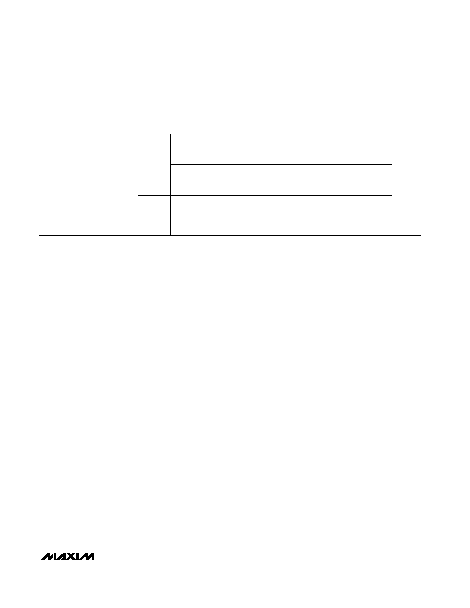
1
1
2
4
3
V
CC
MR
(RESET) RESET
GND
MAX811
MAX812
SOT143
TOP VIEW
( ) ARE FOR MAX812
NOTE: SEE LAST PAGE FOR MARKING INFORMATION.
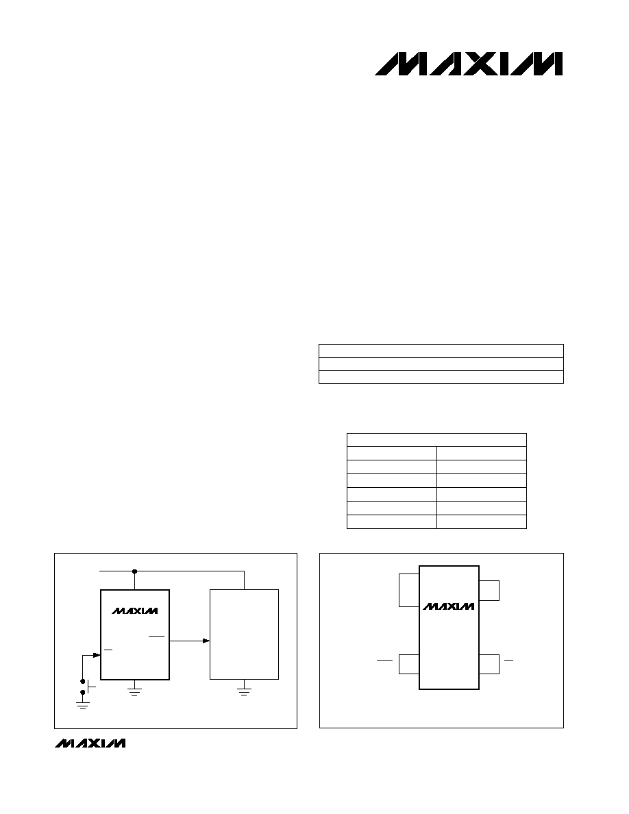
___________________Pin Configuration
MAX811
MAX812
V
CC
V
CC
RESET
(RESET)
RESET
INPUT
GND
V
CC
GND
µP
( ) ARE FOR MAX812
PUSHBUTTON
SWITCH
MR
___________Typical Operating Circuit
19-0411; Rev 3; 3/99
PART*
MAX811_EUS-T
MAX812_EUS-T
-40∞C to +85∞C
-40∞C to +85∞C
TEMP. RANGE
PIN-PACKAGE
4 SOT143
4 SOT143
_______________Ordering Information
* This part offers a choice of five different reset threshold
voltages. Select the letter corresponding to the desired
nominal reset threshold voltage, and insert it into the blank
to complete the part number.
RESET THRESHOLD
SUFFIX
VOLTAGE (V)
L
4.63
M
4.38
T
3.08
S
2.93
R
2.63
For free samples & the latest literature: http://www.maxim-ic.com, or phone 1-800-998-8800.
For small orders, phone 1-800-835-8769.

MAX811/MAX812
4-Pin µP Voltage Monitors
with Manual Reset Input
2
_______________________________________________________________________________________
ABSOLUTE MAXIMUM RATINGS
ELECTRICAL CHARACTERISTICS
(V
CC
= 5V for L/M versions, V
CC
= 3.3V for T/S versions, V
CC
= 3V for R version, T
A
= -40∞C to +85∞C, unless otherwise noted.
Typical values are at T
A
= +25∞C.) (Note 1)
Stresses beyond those listed under "Absolute Maximum Ratings" may cause permanent damage to the device. These are stress ratings only, and functional
operation of the device at these or any other conditions beyond those indicated in the operational sections of the specifications is not implied. Exposure to
absolute maximum rating conditions for extended periods may affect device reliability.
Terminal Voltage (with respect to GND)
V
CC
......................................................................-0.3V to 6.0V
All Other Inputs.......................................-0.3V to (V
CC
+ 0.3V)
Input Current, V
CC,
MR .......................................................20mA
Output Current, RESET or RESET .......................................20mA
Continuous Power Dissipation (T
A
= +70∞C)
SOT143 (derate 4mW/∞C above +70∞C)
320mW
Operating Temperature Range ...........................-40∞C to +85∞C
Storage Temperature Range .............................-65∞C to +160∞C
Lead Temperature (soldering, 10sec) .............................+300∞C
I
SOURCE
= 150µA, 1.8V < V
CC
< V
TH(MIN)
MAX81_R/S/T, V
CC
= 3.6V, I
OUT
= 0
MAX81_L/M, V
CC
= 5.5V, I
OUT
= 0
T
A
= -40∞C to +85∞C
V
OD
= 125mV, MAX81_R/S/T
V
OD
= 125mV, MAX81_L/M
MAX81_S
MAX81_L
MAX81_M
V
CC
= V
TH(MAX)
CONDITIONS
0.8V
CC
2.3
V
IH
µs
0.5
t
MD
MR to Reset Propagation Delay
(Note 2)
ns
100
MR Glitch Immunity (Note 3)
µs
10
t
MR
MR Minimum Pulse Width
ms
140
560
t
RP
Reset Active Timeout Period
µA
2.7
10
I
CC
Supply Current
6
15
V
1.2
V
CC
Operating Voltage Range
µs
20
V
CC
to Reset Delay (Note 2)
40
2.88
2.93
2.98
3.03
3.08
3.14
Reset Threshold
4.54
4.63
4.72
4.50
4.75
4.30
4.38
4.46
4.25
4.50
UNITS
MIN
TYP
MAX
SYMBOL
PARAMETER
MAX812L/M only, I
SINK
= 3.2mA,
V
CC
= V
TH(MAX)
MAX812R/S/T only, I
SINK
= 1.2mA,
V
CC
= V
TH(MAX)
V
0.4
V
OL
RESET Output Voltage
(MAX812)
0.3
V
OH
V
CC
> V
TH(MAX)
, MAX81_L/M
0.8
V
IL
V
CC
> V
TH(MAX)
, MAX81_R/S/T
V
0.25 x V
CC
V
IL
MR Input Threshold
0.7 x V
CC
V
IH
k
10
20
30
MR Pull-Up Resistance
T
A
= 0∞C to +70∞C
1.0
5.5
3.00
3.15
2.85
3.00
ppm/∞C
30
Reset Threshold Tempco
MAX81_R
2.58
2.63
2.68
2.55
2.70
T
A
= +25∞C
T
A
= -40∞C to +85∞C
T
A
= +25∞C
T
A
= -40∞C to +85∞C
MAX81_T
T
A
= +25∞C
T
A
= -40∞C to +85∞C
T
A
= +25∞C
T
A
= -40∞C to +85∞C
T
A
= +25∞C
T
A
= -40∞C to +85∞C
V
TH
V
MAX811/MAX812
4-Pin µP Voltage Monitors
with Manual Reset Input
_______________________________________________________________________________________
3
ELECTRICAL CHARACTERISTICS (continued)
(V
CC
= 5V for L/M versions, V
CC
= 3.3V for T/S versions, V
CC
= 3V for R version, T
A
= -40∞C to +85∞C, unless otherwise noted.
Typical values are at T
A
= +25∞C.) (Note 1)
Note 1: Production testing done at T
A
= +25∞C, over temperature limits guaranteed by design using six sigma design limits.
Note 2: RESET output for MAX811, RESET output for MAX812.
Note 3: "Glitches" of 100ns or less typically will not generate a reset pulse.
MAX811R/S/T only, I
SINK
= 1.2mA,
V
CC
= V
TH(MIN)
MAX811L/M only, I
SOURCE
= 800µA,
V
CC
> V
TH(MAX)
MAX811L/M only, I
SINK
= 3.2mA,
V
CC
= V
TH(MIN)
I
SINK
= 50µA, V
CC
> 1.0V
MAX811R/S/T only, I
SOURCE
= 500µA,
V
CC
> V
TH(MAX)
CONDITIONS
0.3
V
V
CC
- 1.5
V
OH
RESET Output Voltage
(MAX811)
0.4
0.3
V
OL
0.8V
CC
UNITS
MIN
TYP
MAX
SYMBOL
PARAMETER

MAX811/MAX812
4-Pin µP Voltage Monitors
with Manual Reset Input
4
_______________________________________________________________________________________
190
POWER-UP RESET TIMEOUT
vs. TEMPERATURE
230
MAX811/12-TOC5
TEMPERATURE (∞C)
POWER-UP RESET TIMEOUT (ms)
210
200
220
-40
85
35
-15
10
60
MAX81_R/S/T
MAX81_L/M
RESET THRESHOLD DEVIATION
vs. TEMPERATURE
0.9995
1.0000
1.0005
MAX811/12-TOC6
TEMPERATURE (∞C)
NORMALIZED THRESHOLD (V) 0.9985
0.9980
0.9990
-40
85
35
-15
10
60
0
POWER-DOWN RESET DELAY vs. TEMPERATURE
(MAX81_L/M)
200
MAX811/12-TOC4
TEMPERATURE (∞C)
POWER-DOWN RESET DELAY (
µ
s)
100
50
150
-40
85
10
-15
60
35
V
OD
= V
TH
- V
CC
V
OD
= 125mV
V
OD
= 200mV
V
OD
= 20mV
__________________________________________Typical Operating Characteristics
(T
A
= +25∞C, unless otherwise noted.)
0
-40
85
SUPPLY CURRENT vs. TEMPERATURE
(MAX81_R/S/T)
2.0
2.5
3.0
MAX811/12-TOC1
TEMPERATURE (∞C)
SUPPLY CURRENT (µA)
10
1.0
0.5
-15
60
1.5
35
V
CC
= 3.6V
V
CC
= 3.3V
V
CC
= 1V
0
SUPPLY CURRENT vs. TEMPERATURE
(MAX81_L/M)
8
MAX811/12-TOC2
TEMPERATURE (∞C)
SUPPLY CURRENT (µA)
4
2
6
-40
85
10
-15
60
35
V
CC
= 5.5V
V
CC
= 3V
V
CC
= 1V
0
POWER-DOWN RESET DELAY vs. TEMPERATURE
(MAX81_R/S/T)
80
100
MAX811/12-TOC3
TEMPERATURE (∞C)
POWER-DOWN RESET DELAY (
µ
s)
40
20
60
-40
85
10
-15
60
35
V
OD
= V
TH
- V
CC
V
OD
= 20mV
V
OD
= 200mV
V
OD
= 125mV

MAX811/MAX812
4-Pin µP Voltage Monitors
with Manual Reset Input
_______________________________________________________________________________________
5
______________________________________________________________ Pin Description
_______________ Detailed Description
Reset Output
A microprocessor's (µP's) reset input starts the µP in a
known state. These µP supervisory circuits assert reset
to prevent code execution errors during power-up,
power-down, or brownout conditions.
RESET is guaranteed to be a logic low for V
CC
> 1V.
Once V
CC
exceeds the reset threshold, an internal
timer keeps RESET low for the reset timeout period;
after this interval, RESET goes high.
If a brownout condition occurs (V
CC
dips below the
reset threshold), RESET goes low. Any time V
CC
goes
below the reset threshold, the internal timer resets to
zero, and RESET goes low. The internal timer starts
after V
CC
returns above the reset threshold, and RESET
remains low for the reset timeout period.
The manual reset input (MR) can also initiate a reset.
See the Manual Reset Input section.
The MAX812 has an active-high RESET output that is
the inverse of the MAX811's RESET output.
Manual Reset Input
Many µP-based products require manual reset capabil-
ity, allowing the operator, a test technician, or external
logic circuitry to initiate a reset. A logic low on MR
asserts reset. Reset remains asserted while MR is low,
and for the Reset Active Timeout Period (t
RP
) after MR
returns high. This input has an internal 20k
pull-up
resistor, so it can be left open if it is not used. MR can
be driven with TTL or CMOS-logic levels, or with open-
drain/collector outputs. Connect a normally open
momentary switch from MR to GND to create a manual-
reset function; external debounce circuitry is not
required. If MR is driven from long cables or if the
device is used in a noisy environment, connecting a
0.1µF capacitor from MR to ground provides additional
noise immunity.
Reset Threshold Accuracy
The MAX811/MAX812 are ideal for systems using a 5V
±5% or 3V ±5% power supply with ICs specified for 5V
±10% or 3V ±10%, respectively. They are designed to
meet worst-case specifications over temperature. The
reset is guaranteed to assert after the power supply
falls out of regulation, but before power drops below
the minimum specified operating voltage range for the
system ICs. The thresholds are pre-trimmed and exhibit
tight distribution, reducing the range over which an
undesirable reset may occur.
Manual Reset Input. A logic low on MR asserts reset. Reset remains asserted as long as MR is
low and for 180ms after MR returns high. This active-low input has an internal 20k
pull-up
resistor. It can be driven from a TTL or CMOS-logic line, or shorted to ground with a switch.
Leave open if unused.
3
3
+5V, +3.3V, or +3V Supply Voltage
4
4
Active-High Reset Output. RESET remains high while V
CC
is below the reset threshold or while
MR is held low. RESET remains high for Reset Active Timeout Period (t
RP
) after the reset condi-
tions are terminated.
2
--
Active-Low Reset Output. RESET remains low while V
CC
is below the reset threshold or while
MR is held low. RESET remains low for the Reset Active Timeout Period (t
RP
) after the reset
conditions are terminated.
--
2
Ground
1
1
FUNCTION
PIN
MR
V
CC
RESET
RESET
GND
NAME
MAX811
MAX812