 | ÐлекÑÑоннÑй компоненÑ: MAX9722A | СкаÑаÑÑ:  PDF PDF  ZIP ZIP |
Äîêóìåíòàöèÿ è îïèñàíèÿ www.docs.chipfind.ru
General Description
The MAX9722A/MAX9722B stereo headphone amplifiers
are designed for portable equipment where board space
is at a premium. The MAX9722A/MAX9722B use a
unique, patented DirectDrive architecture to produce a
ground-referenced output from a single supply, eliminat-
ing the need for large DC-blocking capacitors, which
saves cost, board space, and component height.
Additionally, the gain of the amplifier is set internally
(-2V/V, MAX9722B) or adjusted externally (MAX9722A).
The MAX9722A/MAX9722B deliver up to 70mW per
channel into a 16
load or 130mW into a 32 load and
have low 0.009% THD+N. An 80dB at 217Hz power-sup-
ply rejection ratio (PSRR) allows these devices to operate
from noisy digital supplies without an additional linear
regulator. The MAX9722A/MAX9722B include ±8kV ESD
protection on the headphone outputs. Comprehensive
anticlick-and-pop circuitry suppresses audible clicks
and pops on startup and shutdown. A low-power shut-
down mode reduces the supply current to 0.1µA.
The MAX9722A/MAX9722B operate from a single 2.4V
to 5.5V supply, consume only 5.5mA of supply current,
feature short-circuit and thermal-overload protection,
and are specified over the extended -40°C to +85°C
temperature range. The devices are available in tiny
16-pin thin QFN (3mm
3mm
0.8mm) and 16-pin
TSSOP packages.
Applications
Features
o 2.4V to 5.5V Single-Supply Operation
o High PSRR (80dB at 217Hz) Eliminates LDO
o No Bulky DC-Blocking Capacitors Required
o Ground-Referenced Outputs Eliminate DC Bias
Voltage on Headphone Ground Pin
o No Degradation of Low-Frequency Response Due
to Output Capacitors
o Differential Inputs for Enhanced Noise
Cancellation
o Adjustable Gain (MAX9722A) or Fixed -2V/V Gain
(MAX9722B)
o 130mW per Channel into 32
o Low 0.009% THD+N
o Integrated Click-and-Pop Suppression
o Low Quiescent Current (5.5mA)
o Short-Circuit and Thermal-Overload Protection
o ±8kV ESD-Protected Amplifier Outputs (Human
Body Model)
o Available in a Space-Saving 16-Pin Thin QFN
(3mm
3mm
0.8mm) Package
MAX9722A/MAX9722B
5V, Differential Input, DirectDrive, 130mW
Stereo Headphone Amplifiers with Shutdown
________________________________________________________________ Maxim Integrated Products
1
Ordering Information
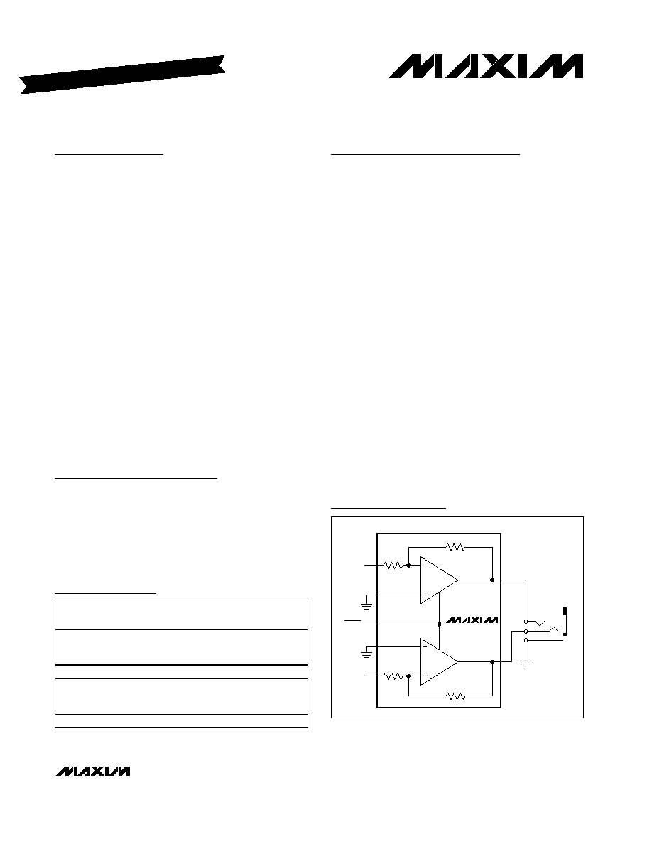
LEFT
AUDIO
INPUT
DirectDrive OUTPUTS
ELIMINATE DC-BLOCKING
CAPACITORS.
FIXED GAIN ELIMINATES
EXTERNAL RESISTOR
NETWORK.
RIGHT
AUDIO
INPUT
SHDN
MAX9722B
Simplified Diagram
19-3049; Rev 0; 10/03
For pricing, delivery, and ordering information, please contact Maxim/Dallas Direct! at
1-888-629-4642, or visit Maxim's website at www.maxim-ic.com.
*EP = Exposed paddle.
Pin Configurations and Typical Operating Circuit appear at
end of data sheet.
PART
TEMP RANGE
PIN-PACKAGE
TOP
MARK
MAX9722AETE -40
°C to +85°C
16 Thin QFN-EP*
(3mm
3mm
0.8mm)
AAX
MAX9722AEUE -40
°C to +85°C 16 TSSOP
--
MAX9722BETE -40
°C to +85°C
16 Thin QFN-EP*
(3mm
3mm
0.8mm)
AAY
MAX9722BEUE -40
°C to +85°C 16 TSSOP
--
Notebook and
Desktop PCs
MP3 Players
Flat-Panel Monitors
Cellular Phones
Smart Phones
PDAs
Portable Audio
Equipment
EVALUATION KIT AVAILABLE
MAX9722A/MAX9722B
5V, Differential Input, DirectDrive, 130mW
Stereo Headphone Amplifiers with Shutdown
2
_______________________________________________________________________________________
ABSOLUTE MAXIMUM RATINGS
ELECTRICAL CHARACTERISTICS
(PV
DD
= SV
DD
= +5V, PGND = SGND = 0V, SHDN = SV
DD
, C1 = C2 = 1µF, R
L
=
, resistive load referenced to ground, for
MAX9722A gain = -1V/V (R
IN
= R
F
= 10k
), for MAX9722B gain = -2V/V (internally set), T
A
= -40°C to +85°C, unless otherwise noted.
Typical values are at T
A
= +25°C, unless otherwise noted.) (Note 1)
Stresses beyond those listed under "Absolute Maximum Ratings" may cause permanent damage to the device. These are stress ratings only, and functional
operation of the device at these or any other conditions beyond those indicated in the operational sections of the specifications is not implied. Exposure to
absolute maximum rating conditions for extended periods may affect device reliability.
PGND to SGND .....................................................-0.3V to +0.3V
PV
DD
and SV
DD
to PGND or SGND .........................-0.3V to +6V
PV
SS
and SV
SS
to PGND ..........................................+0.3V to -6V
IN_ to SGND ................................(SV
SS
- 0.3V) to (SV
DD
+ 0.3V)
OUT_ to PGND ......................................................-3.0V to +3.0V
SHDN to SGND..........................(SGND - 0.3V) to (SV
DD
+ 0.3V)
C1P to PGND ...........................................-0.3V to (PV
DD
+ 0.3V)
C1N to PGND............................................(SV
SS
- 0.3V) to +0.3V
PV
DD
to SV
DD
...........................................................................0V
PV
SS
to SV
SS
............................................................................0V
Output Short Circuit to GND.......................................Continuous
Continuous Power Dissipation (T
A
= +70
°C)
16-Pin Thin QFN (derate 14.7mW/°C above +70°C)....1176mW
16-Pin TSSOP (derate 9.4mW/°C above +70°C) .........755mW
Junction Temperature ......................................................+150°C
Operating Temperature Range............................-40°C to +85°C
Storage Temperature Range .............................-65°C to +150°C
Lead Temperature (soldering, 10s) .................................+300°C
PARAMETER
SYMBOL
CONDITIONS
MIN
TYP
MAX
UNITS
GENERAL
Supply Voltage Range
V
DD
Guaranteed by PSRR test
2.4
5.5
V
Quiescent Supply Current
I
DD
R
L
=
5.5
13
mA
Shutdown Supply Current
I
SHDN
SHDN = SGND
0.1
2
µA
SHDN Input Logic High
V
IH
2
V
SHDN Input Logic Low
V
IL
0.8
V
SHDN Input Leakage Current
-1
+0.05
+1
µA
SHDN to Full Operation Time
t
SON
80
µs
AMPLIFIERS
Voltage Gain
A
V
MAX9722B (Note 2)
-1.98
-2
-2.02
V/V
Gain Matching
MAX9722B, between the right and left channels
±2
%
Between IN_+ and IN_-, AC-coupled (MAX9722A)
±0.5
±2.5
Input Offset Voltage
V
IS
Between IN_+ and IN_-, AC-coupled (MAX9722B)
±1.5
±5
mV
Input Bias Current
I
BIAS
IN_+ and IN_-
50
nA
Input Impedance
R
IN
MAX9722B, measured at IN_
10
14.4
20
k
Input Common-Mode Voltage
Range
V
CM
-0.5
+0.7
V
Common-Mode Rejection Ratio
CMRR
Input referred, MAX9722A, T
A
= +25°C
-60
-70
dB
DC, V
DD
= 2.4V to 5.5V, input referred
-80
-90
f = 217Hz, 100mV
P-P
ripple, input referred
-80
Power-Supply Rejection Ratio
(Note 3)
PSRR
f = 10kHz, 100mV
P-P
ripple, input referred
-50
dB
R
L
= 16
, THD+N = 1%, T
A
= +25°C
60
70
Output Power
P
OUT
R
L
= 32
, THD+N = 1%, T
A
= +25°C
130
mW
Output Voltage
V
OUT
R
L
= 1k
2
V
RMS
Output Impedance in Shutdown
10
k
MAX9722A/MAX9722B
5V, Differential Input, DirectDrive, 130mW
Stereo Headphone Amplifiers with Shutdown
_______________________________________________________________________________________
3
ELECTRICAL CHARACTERISTICS (continued)
(PV
DD
= SV
DD
= +5V, PGND = SGND = 0V, SHDN = SV
DD
, C1 = C2 = 1µF, R
L
=
, resistive load referenced to ground, for
MAX9722A gain = -1V/V (R
IN
= R
F
= 10k
), for MAX9722B gain = -2V/V (internally set), T
A
= -40°C to +85°C, unless otherwise noted.
Typical values are at T
A
= +25°C, unless otherwise noted.) (Note 1)
Note 1: All specifications are 100% tested at T
A
= +25
°C; temperature limits are guaranteed by design.
Note 2: Gain for the MAX9722A is adjustable.
Note 3: The amplifier inputs are AC-coupled to ground through C
IN
_.
Note 4: Measurement bandwidth is 22Hz to 22kHz.
PARAMETER
SYMBOL
CONDITIONS
MIN
TYP
MAX
UNITS
R
L
= 16
, P
OUT
= 55mW, f = 1kHz
0.03
Total Harmonic Distortion Plus
Noise (Note 4)
THD+N
R
L
= 32
, P
OUT
= 125mW, f = 1kHz
0.009
%
Signal-to-Noise Ratio
SNR
R
L
= 32
, P
OUT
= 20mW, f = 22Hz to 22kHz
100
dB
Noise
V
n
22Hz to 22kHz bandwidth, input AC grounded
6
µV
RMS
Slew Rate
SR
0.5
V/µs
Maximum Capacitive Load
C
L
No sustained oscillation
200
pF
Charge-Pump Oscillator
Frequency
f
OSC
505
600
800
kHz
Crosstalk
R
L
= 32
, V
IN
= 200mV
P-P
, f = 10kHz, A
V
= 1
78
dB
ESD Protection
Human Body Model (OUTR and OUTL)
±8
kV
Thermal-Shutdown Threshold
145
°C
Thermal-Shutdown Hysteresis
5
°C
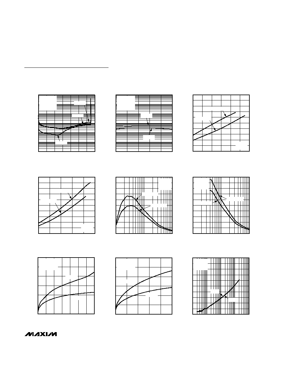
Typical Operating Characteristics
(MAX9722A, PV
DD
= SV
DD
= +5V, PGND = SGND = 0V, SHDN = SV
DD
, C1 = C2 = 1µF, R
L
=
, gain = -1V/V, single-ended input,
THD+N measurement bandwidth = 22Hz to 22kHz, T
A
= +25
°C, unless otherwise noted.)
TOTAL HARMONIC DISTORTION PLUS
NOISE vs. FREQUENCY
MAX9722 toc01
FREQUENCY (Hz)
THD+N (%)
10k
1k
100
0.001
0.01
0.1
1
10
0.0001
10
100k
V
DD
= 3V
A
V
= -1V/V
R
L
= 16
P
OUT
= 30mW
P
OUT
= 5mW
P
OUT
= 15mW
TOTAL HARMONIC DISTORTION PLUS
NOISE vs. FREQUENCY
MAX9722 toc02
FREQUENCY (Hz)
THD+N (%)
10k
1k
100
0.001
0.01
0.1
1
10
0.0001
10
100k
V
DD
= 3V
A
V
= -1V/V
R
L
= 32
P
OUT
= 40mW
P
OUT
= 5mW
P
OUT
= 20mW
TOTAL HARMONIC DISTORTION PLUS
NOISE vs. FREQUENCY
MAX9722 toc03
FREQUENCY (Hz)
THD+N (%)
10k
1k
100
0.001
0.01
0.1
1
10
0.0001
10
100k
V
DD
= 5V
A
V
= -1V/V
R
L
= 16
P
OUT
= 40mW
P
OUT
= 5mW
P
OUT
= 60mW
MAX9722A/MAX9722B
5V, Differential Input, DirectDrive, 130mW
Stereo Headphone Amplifiers with Shutdown
4
_______________________________________________________________________________________
Typical Operating Characteristics (continued)
(MAX9722A, PV
DD
= SV
DD
= +5V, PGND = SGND = 0V, SHDN = SV
DD
, C1 = C2 = 1µF, R
L
=
, gain = -1V/V, single-ended input,
THD+N measurement bandwidth = 22Hz to 22kHz, T
A
= +25°C, unless otherwise noted.)
TOTAL HARMONIC DISTORTION PLUS
NOISE vs. FREQUENCY
MAX9722 toc04
FREQUENCY (Hz)
THD+N (%)
10k
1k
100
0.001
0.01
0.1
1
10
0.0001
10
100k
V
DD
= 5V
A
V
= -2V/V
R
L
= 16
P
OUT
= 40mW
P
OUT
= 5mW
P
OUT
= 20mW
TOTAL HARMONIC DISTORTION PLUS
NOISE vs. FREQUENCY
MAX9722 toc05
FREQUENCY (Hz)
THD+N (%)
10k
1k
100
0.001
0.01
0.1
1
10
0.0001
10
100k
V
DD
= 5V
A
V
= -1V/V
R
L
= 32
P
OUT
= 80mW
P
OUT
= 5mW
P
OUT
= 20mW
TOTAL HARMONIC DISTORTION PLUS
NOISE vs. FREQUENCY
MAX9722 toc06
FREQUENCY (Hz)
THD+N (%)
10k
1k
100
0.001
0.01
0.1
1
10
0.0001
10
100k
V
DD
= 5V
A
V
= -2V/V
R
L
= 32
P
OUT
= 80mW
P
OUT
= 5mW
P
OUT
= 20mW
TOTAL HARMONIC DISTORTION PLUS
NOISE vs. OUTPUT POWER
MAX9722 toc07
OUTPUT POWER (mW)
THD+N (%)
60
50
40
30
20
10
0.001
0.01
0.1
1
10
100
0.0001
0
70
f = 10kHz
f = 20Hz
f = 1kHz
V
DD
= 3V
A
V
= -1V/V
R
L
= 16
TOTAL HARMONIC DISTORTION PLUS
NOISE vs. OUTPUT POWER
MAX9722 toc08
OUTPUT POWER (mW)
THD+N (%)
60
70
50
40
30
20
10
0.001
0.01
0.1
1
10
100
0.0001
0
80
f = 10kHz
f = 20Hz
f = 1kHz
V
DD
= 3V
A
V
= -1V/V
R
L
= 32
TOTAL HARMONIC DISTORTION PLUS
NOISE vs. OUTPUT POWER
MAX9722 toc09
OUTPUT POWER (mW)
THD+N (%)
60
50
40
30
20
10
0.001
0.01
0.1
1
10
100
0.0001
0
70
f = 10kHz
f = 20Hz
f = 1kHz
V
DD
= 5V
A
V
= -1V/V
R
L
= 16
TOTAL HARMONIC DISTORTION PLUS
NOISE vs. OUTPUT POWER
MAX9722 toc10
OUTPUT POWER (mW)
THD+N (%)
60
50
40
30
20
10
0.001
0.01
0.1
1
10
100
0.0001
0
70
f = 10kHz
f = 20Hz
f = 1kHz
V
DD
= 5V
A
V
= -2V/V
R
L
= 16
TOTAL HARMONIC DISTORTION PLUS
NOISE vs. OUTPUT POWER
MAX9722 toc11
OUTPUT POWER (mW)
THD+N (%)
120
100
80
60
40
20
0.001
0.01
0.1
1
10
100
0.0001
0
140
f = 10kHz
f = 20Hz
f = 1kHz
V
DD
= 5V
A
V
= -1V/V
R
L
= 32
TOTAL HARMONIC DISTORTION PLUS
NOISE vs. OUTPUT POWER
MAX9722 toc12
OUTPUT POWER (mW)
THD+N (%)
120
100
80
60
40
20
0.001
0.01
0.1
1
10
100
0.0001
0
140
f = 10kHz
f = 20Hz
f = 1kHz
V
DD
= 5V
A
V
= -2V/V
R
L
= 32
MAX9722A/MAX9722B
5V, Differential Input, DirectDrive, 130mW
Stereo Headphone Amplifiers with Shutdown
_______________________________________________________________________________________
5
TOTAL HARMONIC DISTORTION PLUS
NOISE vs. OUTPUT POWER
MAX9722 toc13
OUTPUT POWER (mW)
THD+N (%)
60
50
40
30
20
10
0.001
0.01
0.1
1
10
100
0.0001
0
70
f = 10kHz
f = 20Hz
f = 1kHz
V
DD
= 5V
A
V
= -1V/V
R
L
= 16
DIFFERENTIAL
TOTAL HARMONIC DISTORTION PLUS
NOISE vs. COMMON-MODE VOLTAGE
MAX9722 toc14
COMMON-MODE VOLTAGE (V)
THD+N (%)
0.3
0.1
-0.1
-0.3
0.001
0.01
0.1
1
10
100
0.0001
-0.5
0.5
R
L
= 16
R
L
= 32
V
DD
= 5V
A
V
= -1V/V
f = 1kHz
DIFFERENTIAL
OUTPUT POWER
vs. SUPPLY VOLTAGE
MAX9722 toc15
SUPPLY VOLTAGE (V)
OUTPUT POWER (mW)
3.4
3.2
3.0
2.8
2.6
10
20
30
40
50
60
70
80
90
100
0
2.4
3.6
THD+N = 10%
THD+N = 1%
f = 1kHz
R
L
= 16
OUTPUT POWER
vs. SUPPLY VOLTAGE
MAX9722 toc16
SUPPLY VOLTAGE (V)
OUTPUT POWER (mW)
4.4
3.9
3.4
2.9
20
40
60
80
100
120
140
160
180
200
0
2.4
4.9
THD+N = 10%
THD+N = 1%
f = 1kHz
R
L
= 32
OUTPUT POWER
vs. LOAD RESISTANCE
MAX9722 toc17
LOAD RESISTANCE (
)
OUTPUT POWER (mW)
100
10
20
30
40
50
60
70
80
90
100
0
10
1000
THD+N = 10%
THD+N = 1%
V
DD
= 3V
f = 1kHz
A
V
= -1V/V
OUTPUT POWER
vs. LOAD RESISTANCE
MAX9722 toc18
LOAD RESISTANCE (
)
OUTPUT POWER (mW)
100
20
40
60
80
100
120
140
160
180
200
0
10
1000
V
DD
= 5V
f = 1kHz
A
V
= -1V/V
THD+N = 1%
THD+N = 10%
POWER DISSIPATION
vs. OUTPUT POWER
MAX9722 toc19
OUTPUT POWER (mW)
POWER DISSIPATION (mW)
60
50
40
30
20
10
50
100
150
200
250
300
0
0
70
V
DD
= 3V
f = 1kHz
P
OUT
= P
L
+ P
R
R
L
= 16
R
L
= 32
POWER DISSIPATION
vs. OUTPUT POWER
MAX9722 toc20
OUTPUT POWER (mW)
POWER DISSIPATION (mW)
80
60
40
20
100
200
300
400
500
600
0
0
100
V
DD
= 5V
f = 1kHz
P
OUT
= P
L
+ P
R
R
L
= 16
R
L
= 32
POWER-SUPPLY REJECTION RATIO
vs. FREQUENCY
MAX9722 toc21
FREQUENCY (Hz)
PSRR (dB)
10k
1k
100
-90
-80
-70
-60
-50
-40
-30
-20
-10
0
-100
10
100k
V
DD
= 3V
A
V
= -1V/V
R
L
= 32
RIGHT
LEFT
Typical Operating Characteristics (continued)
(MAX9722A, PV
DD
= SV
DD
= +5V, PGND = SGND = 0V, SHDN = SV
DD
, C1 = C2 = 1µF, R
L
=
, gain = -1V/V, single-ended input,
THD+N measurement bandwidth = 22Hz to 22kHz, T
A
= +25°C, unless otherwise noted.)