 | –≠–ª–µ–∫—Ç—Ä–æ–Ω–Ω—ã–π –∫–æ–º–ø–æ–Ω–µ–Ω—Ç: MXB7846 | –°–∫–∞—á–∞—Ç—å:  PDF PDF  ZIP ZIP |

General Description
The MXB7846 is an industry-standard 4-wire touch-
screen controller. It contains a 12-bit sampling analog-
to-digital converter (ADC) with a synchronous serial
interface and low on-resistance switches for driving
resistive touch screens. The MXB7846 uses an internal
+2.5V reference or an external reference. The
MXB7846 can make absolute or ratiometric measure-
ments. In addition, this device has an on-chip tempera-
ture sensor, a battery-monitoring channel, and has the
ability to perform touch-pressure measurements without
external components. The MXB7846 has one auxiliary
ADC input. All analog inputs are fully ESD protected,
eliminating the need for external TransZorbTM devices.
The MXB7846 is guaranteed to operate with a supply
voltage down to +2.375V when used with an external
reference or +2.7V with an internal reference. In shut-
down mode, the typical power consumption is reduced
to under 0.5µW, while the typical power consumption at
125ksps throughput and a +2.7V supply is 650µW.
Low-power operation makes the MXB7846 ideal for bat-
tery-operated systems, such as personal digital assis-
tants with resistive touch screens and other portable
equipment. The MXB7846 is available in 16-pin QSOP
and TSSOP packages, and is guaranteed over the
-40∞C to +85∞C temperature range.
Applications
Personal Digital Assistants
Portable Instruments
Point-of-Sales Terminals
Pagers
Touch-Screen Monitors
Cellular Phones
Features
ESD-Protected ADC Inputs
±15kV IEC 61000-4-2 Air-Gap Discharge
±8kV IEC 61000-4-2 Contact Discharge
Pin Compatible with MXB7843
+2.375V to +5.25V Single Supply
Internal +2.5V Reference
Direct Battery Measurement (0 to 6V)
On-Chip Temperature Measurement
Touch-Pressure Measurement
4-Wire Touch-Screen Interface
Ratiometric Conversion
SPITM/QSPITM, 3-Wire Serial Interface
Programmable 8-/12-Bit Resolution
Auxiliary Analog Input
Automatic Shutdown Between Conversions
Low Power (External Reference)
270µA at 125ksps
115µA at 50ksps
25µA at 10ksps
5µA at 1ksps
2µA Shutdown Current
MXB7846
2.375V to 5.25V, 4-Wire Touch-Screen Controller
with Internal Reference and Temperature Sensor
________________________________________________________________ Maxim Integrated Products
1
16
15
14
13
12
11
10
9
1
2
3
4
5
6
7
8
V
DD
DCLK
CS
DIN
BUSY
DOUT
PENIRQ
V
DD
REF
TOP VIEW
MXB7846
QSOP/TSSOP
X+
Y+
GND
X-
Y-
BAT
AUX
Pin Configuration
Ordering Information
19-2436; Rev 1; 5/04
For pricing, delivery, and ordering information, please contact Maxim/Dallas Direct! at
1-888-629-4642, or visit Maxim's website at www.maxim-ic.com.
PART
TEMP RANGE
PIN-PACKAGE
MXB7846EEE
-40
∞
C to +85
∞
C
16 QSOP
MXB7846EUE
-40
∞
C to +85
∞
C
16 TSSOP
TransZorb is a trademark of Vishay Intertechnology, Inc.
SPI/QSPI are trademarks of Motorola, Inc.
Typical Application Circuit appears at end of data sheet.

MXB7846
2.375V to 5.25V, 4-Wire Touch-Screen Controller
with Internal Reference and Temperature Sensor
2
_______________________________________________________________________________________
ABSOLUTE MAXIMUM RATINGS
Stresses beyond those listed under "Absolute Maximum Ratings" may cause permanent damage to the device. These are stress ratings only, and functional
operation of the device at these or any other conditions beyond those indicated in the operational sections of the specifications is not implied. Exposure to
absolute maximum rating conditions for extended periods may affect device reliability.
V
DD
, VBAT, DIN, CS, DCLK to GND ........................-0.3V to +6V
Digital Outputs to GND...............................-0.3V to (V
DD
+ 0.3V)
V
REF
, X+, X-, Y+, Y-, AUX to GND..............-0.3V to (V
DD
+ 0.3V)
Maximum Current into Any Pin .........................................±50mA
Maximum ESD per IEC-61000-4-2 (per MIL STD-883 HBM)
X+, X-, Y+, Y-, VBAT, AUX ......................................15kV (4kV)
All Other Pins ..........................................................2kV (500V)
Continuous Power Dissipation (T
A
= +70∞C)
16-Pin QSOP (derate 8.30mW/∞C above +70∞C).........667mW
16-Pin TSSOP (derate 5.70mW/∞C above +70∞C) .......456mW
Operating Temperature Range ...........................-40∞C to +85∞C
Junction Temperature ......................................................+150∞C
Storage Temperature Range .............................-65∞C to +150∞C
Lead Temperature (soldering, 10s) .................................+300∞C
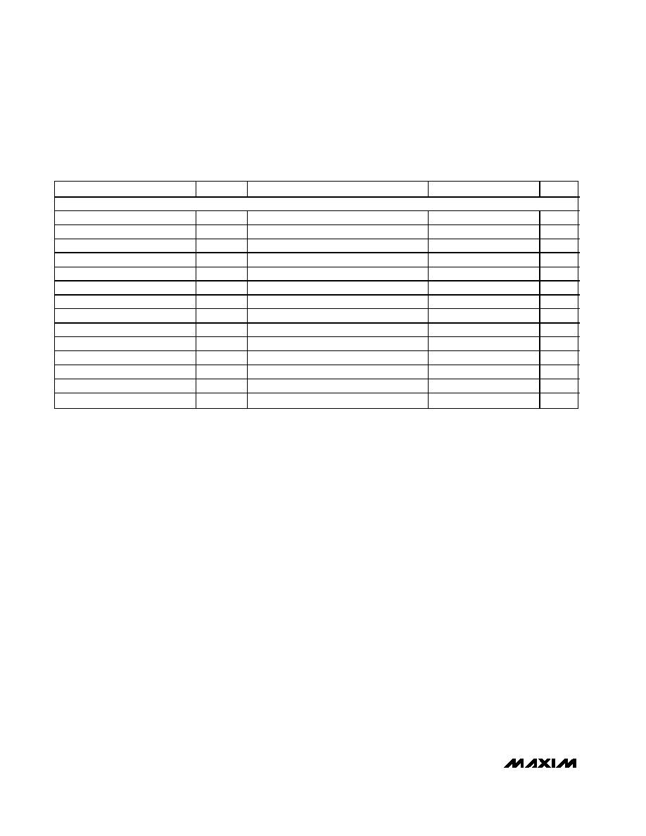
ELECTRICAL CHARACTERISTICS
(V
DD
= 2.7V to 3.6V, V
REF
= 2.5V, f
DCLK
= 2MHz (50% duty cycle), f
SAMPLE
= 125kHz, 12-bit mode, 0.1µF capacitor at REF, T
A
=
T
MIN
to T
MAX
, unless otherwise noted. Typical values are at T
A
= +25∞C.)
PARAMETER
SYM B O L
CONDITIONS
MIN
TYP
MAX
UNITS
DC ACCURACY
(Note 1)
Resolution
12
Bits
No Missing Codes
11
12
Bits
Relative Accuracy
INL
(Note 2)
±1
±2
LSB
Differential Nonlinearity
DNL
±1
LSB
Offset Error
±6
LSB
Gain Error
(Note 3)
±4
LSB
Noise
Including internal reference
70
µV
RMS
CONVERSION RATE
Conversion Time
t
CONV
12 clock cycles (Note 4)
6
µs
Track/Hold Acquisition Time
t
ACQ
3 clock cycles
1.5
µs
Throughput Rate
f
SAMPLE
16 clock conversion
125
kHz
Multiplexer Settling Time
500
ns
Aperture Delay
30
ns
Aperture Jitter
100
p s
Channel-to-Channel Isolation
V
IN
= 2.5V
P-P
at 50kHz
100
dB
Serial Clock Frequency
f
DCLK
0.1
2.0
MHz
Duty Cycle
40
60
%
ANALOG INPUT (X+, X-, Y+, Y-, AUX)
Input Voltage Range
0
V
REF
V
Input Capacitance
25
pF
Input Leakage Current
On/off leakage, V
IN
= 0 to V
DD
±0.1
±1
µA
SWITCH DRIVERS
Y+, X+
7
On-Resistance (Note 5)
Y-, X-
9
INTERNAL REFERENCE
Reference Output Voltage
V
REF
V
DD
= 2.7V to 5.25V, T
A
= +25∞C
2.45
2.50
2.55
V
REF Output Tempco
TCV
REF
50
ppm∞/C
REF Short-Circuit Current
18
mA
REF Output Impedance
250

MXB7846
2.375V to 5.25V, 4-Wire Touch-Screen Controller
with Internal Reference and Temperature Sensor
_______________________________________________________________________________________
3
ELECTRICAL CHARACTERISTICS (continued)
(V
DD
= 2.7V to 3.6V, V
REF
= 2.5V, f
DCLK
= 2MHz (50% duty cycle), f
SAMPLE
= 125kHz, 12-bit mode, 0.1µF capacitor at REF, T
A
=
T
MIN
to T
MAX
, unless otherwise noted. Typical values are at T
A
= +25∞C.)
PARAMETER
SYM B O L
CONDITIONS
MIN
TYP
MAX
UNITS
EXTERNAL REFERENCE
(Internal reference disabled, reference applied to REF)
Reference Input Voltage Range
(Note 7)
1
V
DD
V
Input Resistance
1
G
f
SAMPLE
= 125kHz
13
40
f
SAMPLE
= 12.5kHz
2.5
µA
Input Current
f
DCLK
= 0
±3
BATTERY MONITOR
(BAT)
Input Voltage Range
0
6
V
Input Resistance
During acquisition
10
k
V
REF
= 2.5V
±
2
Accuracy
Internal reference
±
3
%
TEMPERATURE MEASUREMENT
Differential method (Note 8)
1.6
∞C
Resolution
Single-conversion method
0.3
∞C
Differential method (Note 8)
±
2
∞C
Accuracy
Single-conversion method
±
3
∞C
DIGITAL INPUTS (DCLK,
CS
, DIN)
Input High Voltage
V
IH
V
DD
0.7
V
Input Low Voltage
V
IL
0.8
V
Input Hysteresis
V
HYST
100
mV
Input Leakage Current
I
IN
±1
µA
Input Capacitance
C
IN
15
pF
DIGITAL OUTPUT (DOUT, BUSY)
Output Voltage Low
V
OL
I
SINK
= 250µA
0.4
V
Output Voltage High
V
OH
I
SOURCE
= 250µA
V
DD
-
0.5
V
PENIRQ Output Low Voltage
V
OL
50k
pullup to V
DD
0.8
V
Three-State Leakage Current
I
L
CS = V
DD
1
±10
µA
Three-State Output Capacitance
C
OUT
CS = V
DD
15
pF
POWER REQUIREMENTS
External reference
2.375
5.250
Supply Voltage
V
DD
Internal reference
2.70
5.25
V
f
SAMPLE
= 125ksps
270
650
f
SAMPLE
= 12.5ksps
220
External
reference
f
SAMPLE
= 0
150
µA
f
SAMPLE
= 125ksps
780
950
f
SAMPLE
= 12.5ksps
720
Supply Current
I
DD
Internal
reference
f
SAMPLE
= 0
650
µA
Shutdown Supply Current
I
SHDN
DCLK = CS = V
DD
3
µA
Power-Supply Rejection Ratio
P
SRR
V
DD
= 2.7V to 3.6V full scale
70
dB
MXB7846
2.375V to 5.25V, 4-Wire Touch-Screen Controller
with Internal Reference and Temperature Sensor
4
_______________________________________________________________________________________
Note 1:
Tested at V
DD
= 2.7V.
Note 2:
Relative accuracy is the deviation of the analog value at any code from its theoretical value after the full-scale range has
been calibrated.
Note 3:
Offset nulled.
Note 4:
Conversion time is defined as the number of clock cycles multiplied by the clock period; clock has 50% duty cycle.
Note 5:
Resistance measured from the source to drain of the switch.
Note 6:
External load should not change during conversion for specified accuracy.
Note 7:
ADC performance is limited by the conversion noise floor, typically 300µV
P-P
. An external reference below 2.5V can com-
promise the ADC performance.
Note 8:
Difference between Temp0 and Temp1. No calibration necessary.
TIMING CHARACTERISTICS (Figure 1)
(V
DD
= 2.7V to 3.6V, V
REF
= 2.5V, f
DCLK
= 2MHz (50% duty cycle), f
SAMPLE
= 125kHz, 12-bit mode, 0.1µF capacitor at REF, T
A
=
T
MIN
to T
MAX
, unless otherwise noted. Typical values are at T
A
= +25∞C.)
PARAMETER
SYM B O L
CONDITIONS
MIN
TYP
MAX
UNITS
TIMING CHARACTERISTICS
(Figure 1)
Acquisition Time
t
ACQ
1.5
µs
DCLK Clock Period
t
CP
500
ns
DCLK Pulse Width High
t
CH
200
ns
DCLK Pulse Width Low
t
CL
200
ns
DIN-to-DCLK Setup Time
t
DS
100
ns
DIN-to-DCLK Hold Time
t
DH
0
ns
CS Fall-to-DCLK Rise Setup Time
t
CSS
100
ns
CS Rise-to-DCLK Rise Ignore
t
CSH
0
ns
DCLK Falling-to-DOUT Valid
t
DO
C
LOAD
= 50pF
200
ns
CS Rise-to-DOUT Disable
t
TR
C
LOAD
= 50pF
200
ns
CS Fall-to-DOUT Enable
t
DV
C
LOAD
= 50pF
200
ns
DCLK Falling-to-BUSY Rising
t
BD
200
ns
CS Falling-to-BUSY Enable
t
BDV
200
ns
CS Rise-to-BUSY Disable
t
BTR
200
ns

Typical Operating Characteristics
(V
DD
= 2.7V, V
REF
= 2.5V
EXTERNAL
, f
DCLK
= 2MHz, f
SAMPLE
= 125kHz, C
LOAD
= 50pF, 0.1µF capacitor at REF, T
A
= +25∞C, unless
otherwise noted.)
MXB7846
2.375V to 5.25V, 4-Wire Touch-Screen Controller
with Internal Reference and Temperature Sensor
_______________________________________________________________________________________
5
INTEGRAL NONLINEARITY
vs. DIGITAL OUTPUT CODE
MXB7846 toc01
OUTPUT CODE
INL (LSB)
3500
3000
2000 2500
1000 1500
500
-0.3
-0.2
-0.1
0
0.1
0.2
0.3
0.4
0.5
-0.4
0
4000
DIFFERENTIAL NONLINEARITY
vs. DIGITAL OUTPUT CODE
MXB7846 toc02
OUTPUT CODE
DNL (LSB)
3500
3000
2000 2500
1000 1500
500
-0.6
-0.4
-0.2
0
0.2
0.4
0.6
0.8
1.0
-1.0
-0.8
0
4000
CHANGE IN OFFSET ERROR
vs. SUPPLY VOLTAGE
MXB7846 toc04
SUPPLY VOLTAGE (V)
OFFSET ERROR (LSB)
5.0
4.5
3.0
3.5
4.0
-1.5
-1.0
-0.5
0
0.5
1.0
1.5
2.0
-2.0
2.5
5.5
CHANGE IN OFFSET ERROR
vs. TEMPERATURE
MXB7846 toc05
TEMPERATURE (∞C)
OFFSET ERROR FROM +25
∞
C (LSB)
65
50
35
20
5
-10
-25
-0.5
0
0.5
1.0
-1.0
-40
80
CHANGE IN GAIN ERROR
vs. SUPPLY VOLTAGE
MXB7846 toc07
SUPPLY VOLTAGE (V)
GAIN ERROR (LSB)
5.0
4.5
4.0
3.5
3.0
-2
-1
0
1
2
3
-3
2.5
5.5
CHANGE IN GAIN ERROR
vs. TEMPERATURE
MXB7846 toc08
TEMPERATURE (∞C)
GAIN ERROR FROM +25
∞
C (LSB)
65
50
35
20
5
-10
-25
-1.5
-1.0
-0.5
0
0.5
1.0
-2.0
-40
80
SWITCH ON-RESISTANCE vs. SUPPLY VOLTAGE
(X+, Y+ : +V
DD
TO PIN; X-, Y- : TO GND)
MXB7846 toc03
SUPPLY VOLTAGE (V)
R
ON
(
)
5.0
4.5
4.0
3.5
3.0
2
4
6
8
10
12
14
0
2.5
5.5
X-
Y-
X+
Y+
SWITCH ON-RESISTANCE vs. TEMPERATURE
(X+, Y+ : +V
DD
TO PIN; X-, Y- : PIN TO GND)
MXB7846 toc06
TEMPERATURE (∞C)
R
ON
(
)
35
20
5
-10
-25
2
1
3
7
6
5
4
8
9
10
11
12
0
-40
50
65
80
X-
Y-
X+
Y+
INTERNAL REFERENCE
vs. SUPPLY VOLTAGE
MXB7846 toc09
SUPPLY VOLTAGE (V)
INTERNAL REFERENCE (V)
5.0
4.5
4.0
3.5
3.0
2.5
2.1
2.2
2.3
2.4
2.5
2.6
2.0
2.0
5.5
C
L
= 0.1µf