 | –≠–ª–µ–∫—Ç—Ä–æ–Ω–Ω—ã–π –∫–æ–º–ø–æ–Ω–µ–Ω—Ç: MXD1815 | –°–∫–∞—á–∞—Ç—å:  PDF PDF  ZIP ZIP |
General Description
The MXD1810≠MXD1813/MXD1815≠MXD1818 family of
microprocessor (µP) reset circuits monitor power sup-
plies in µP and digital systems. These devices provide
excellent circuit reliability and low cost by eliminating
external components and adjustments when used with
+2.5V/+3.0V/+3.3V (MXD1815≠MXD1818), and +5V
(MXD1810≠MXD1813) systems.
These circuits assert a reset signal whenever the V
CC
supply voltage declines below a preset threshold,
keeping reset asserted for at least 100ms after V
CC
rises above the reset threshold. The MXD1813/
MXD1818 also keep reset asserted for at least 100ms
after the output is momentarily pulled to GND by an
external push-button switch.
The MXD1812/MXD1817 have an active-high push-pull
RESET output. The MXD1810/MXD1815 (push-pull) and
MXD1811/MXD1813/MXD1816/MD1818 (open-drain)
have an active-low RESET output. The open-drain
devices (MXD1811/MXD1813/MXD1816/MXD1818)
have an internal pullup resistor to V
CC
. The
MXD1813/MXD1818 feature a debounced manual reset
feature that asserts a reset if the RESET pin is pulled
low for more than 1.5µs. When used to initiate manual
reset, RESET debounces signals from devices such as
mechanical switches. For devices with this feature, the
release of the external switch triggers the reset period.
The MXD1810≠MXD1813/MXD1815≠MXD1818 are
guaranteed to output the correct logic state for V
CC
down to +1V. These ICs provide a reset comparator
designed to ignore fast transients on V
CC
. Reset
thresholds are available between +2.18V and +4.62V.
These small, low-power (4µA) devices are ideal for use
in portable equipment. All are available in space-saving
3-pin SC70 and SOT23 packages, and are specified
from -40∞C to +105∞C.
Applications
Computers and Controllers
Intelligent Instruments
Set-Top Boxes
Printers
Automotive Systems
Critical µP and µC Monitoring
Portable/Battery-Powered Equipment
Features
o Precision Monitoring of +2.5V, +3V, +3.3V, and
+5V Power-Supply Voltages
o Available in Four Reset Output Configurations
o Factory-Set Reset Threshold Voltages: 2.18V,
2.31V, 2.55V, 2.88V, 3.06V, 4.12V, 4.37V, 4.62V
o ±2.5% Reset Threshold Accuracy Over
Temperature
o Fixed Reset Timeout Period: 100ms (min)
o Guaranteed RESET/RESET Valid to V
CC
= +1V
o Debounced Manual Reset Detect
(MXD1813/MXD1818)
o Power-Supply Transient Immunity
o No External Components
o Low Power Consumption (4µA)
o Pin Compatible with DS181_ Products (SOT23)
o 3-Pin SC70 and SOT23 Packages
MXD1810≠MXD1813/MXD1815≠MXD1818*
Low-Power µP Reset Circuits in 3-Pin
SC70/SOT23
________________________________________________________________ Maxim Integrated Products
1
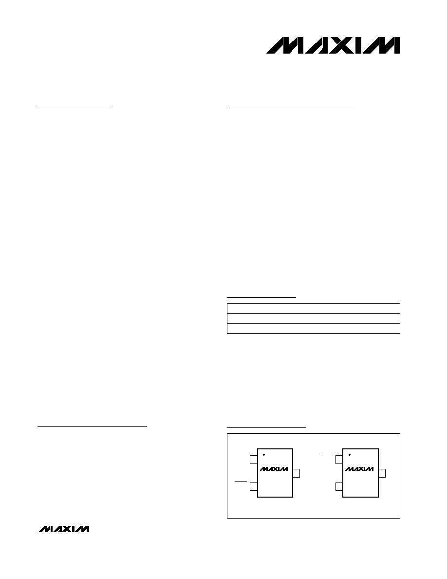
RESET
(RESET)
1
3
GND
V
CC
MXD181_X
SC70-3
TOP VIEW
2
() ARE FOR THE MXD1812/MXD1817
RESET
(RESET)
1
3
GND
V
CC
MXD181_U
SOT23-3
2
Pin Configurations
Ordering Information
19-2243; Rev 0; 10/01
Ordering Information continued at end of data sheet.
For pricing, delivery, and ordering information, please contact Maxim/Dallas Direct! at
1-888-629-4642, or visit Maxim's website at www.maxim-ic.com.
PART
TEMP. RANGE
PIN-PACKAGE
MXD1810UR_ _-T
-40
o
C to +105
o
C
3 SOT23-3
MXD1810XR_ _-T
-40
o
C to +105
o
C
3 SC70-3
The MXD1810≠MXD1813/MXD1815≠MXD1818 are available
with factory-set V
CC
reset thresholds from +2.18V to +3.06V
(MXD1815≠MXD1818) and +4.12V to +4.62V (MXD1810≠
MXD1813). Choose the desired reset-threshold suffix from the
Reset Threshold Table and insert it in place of the "_ _" follow-
ing "R" in the part number. All devices are available in tape-
and-reel only in 2500 unit increments. Other threshold voltages
may be available. Contact factory for availability.
*Patent pending
MXD1810≠MXD1813/MXD1815≠MXD1818
Low-Power µP Reset Circuits in 3-Pin
SC70/SOT23
2
_______________________________________________________________________________________
ABSOLUTE MAXIMUM RATINGS
ELECTRICAL CHARACTERISTICS
(V
CC
= full range, T
A
= -40∞C to +105∞C, unless otherwise specified. Typical values are at T
A
= +25∞C.) (Note 1)
Stresses beyond those listed under "Absolute Maximum Ratings" may cause permanent damage to the device. These are stress ratings only, and functional
operation of the device at these or any other conditions beyond those indicated in the operational sections of the specifications is not implied. Exposure to
absolute maximum rating conditions for extended periods may affect device reliability.
V
CC
to GND ...........................................................-0.3V to +6.0V
Push-Pull RESET (MXD1810/MXD1815),
RESET (MXD1812/MXD1817) to GND.....-0.3V to (V
CC
+ 0.3V)
Open-Drain RESET (MXD1811/MXD1816)
to GND................................................................-0.3V to +6.0V
Open-Drain RESET (MXD1813/MXD1818)
to GND ....................................................-0.3V to (V
CC
+ 0.3V)
Input Current (V
CC
, RESET) ................................................20mA
Output Current (RESET, RESET).........................................20mA
Continuous Power Dissipation (T
A
= +70∞C)
3-Pin SC70 (derate 2.17mW above +70∞C) ..................174mW
3-Pin SOT23 (derate 4mW/∞C above +70∞C) ...............320mW
Operating Temperature Range .........................-40∞C to +105∞C
Junction Temperature ......................................................+150∞C
Storage Temperature Range .............................-65∞C to +150∞C
Lead Temperature (soldering, 10s) .................................+300∞C
PARAMETER
SYMBOL
CONDITIONS
MIN
TYP
MAX
UNITS
T
A
= 0∞C to +105∞C
1.0
5.5
Supply Voltage Range
V
CC
T
A
= -40∞C to +105∞C
1.2
5.5
V
V
CC
= +5.5V, V
CC
> V
TH
, no load
9
16
Supply Current
I
CC
V
CC
= +3.6V, V
CC
> V
TH
, no load
4
10
µA
MXD181_ _ R46
4.50
4.62
4.75
MXD181_ _ R44
4.25
4.37
4.49
MXD181_ _ R41
4.00
4.12
4.24
MXD181_ _ R31
2.98
3.06
3.15
MXD181_ _ R29
2.80
2.88
2.97
MXD181_ _ R26
2.47
2.55
2.64
MXD181_ _ R23
2.25
2.31
2.37
Reset Threshold
V
TH
MXD181_ _ R22
2.12
2.18
2.25
V
Active Reset Timeout Period
t
RP
V
CC
rising
100
150
250
ms
V
CC
= (V
TH
+ 100mV) falling to (V
TH
- 200mV)
2
5
µs
V
CC
to Reset Delay
t
RD
V
CC
rising, t
R
= 5µs
100
150
250
ms
Push-Button Detect to Reset
t
PB
MXD1813/MXD1818 only
1.5
µs
Push-Button Reset Timeout Period
t
PBRST
MXD1813/MXD1818 only
100
150
250
ms
T
A
= +25∞C to +105∞C
0.34
Input Low Voltage
V
IL
MXD1813/MXD1818
only
T
A
= -40∞C to +25∞C
0.15
V
Input High Voltage
V
IH
MXD1813/MXD1818 only
0.7
◊ V
CC
V
RESET Output Source Current
I
OH
V
CC
V
TH(MAX)
, reset not asserted,
MXD1810/MXD1815
350
µA
RESET Output Source Current
I
OH
V
CC
V
TH(MIN)
, reset asserted,
MXD1812/MXD1817
350
µA
RESET Output Sink Current
I
OL
V
CC
2.7V, reset asserted, V
OUT
= 0.4V
MXD1810/MXD1811/MXD1813/MXD1815/
MXD1816/MXD1818
(Note 2)
10
mA
RESET Output Sink Current
I
OL
V
CC
2.7V, reset not asserted, , V
OUT
= 0.4V
MXD1812/MXD1817
10
mA

MXD1810≠MXD1813/MXD1815≠MXD1818
Low-Power µP Reset Circuits in 3-Pin
SC70/SOT23
_______________________________________________________________________________________
3
ELECTRICAL CHARACTERISTICS (continued)
(V
CC
= full range, T
A
= -40∞C to +105∞C, unless otherwise specified. Typical values are at T
A
= +25∞C.) (Note 1)
Note 1: Production testing done at T
A
= +25∞C; limits over temperature guaranteed by design.
Note 2: The MXD1811/MXD1813/MXD1816/MXD1818 have an internal pullup resistor which may deliver 1mA of sink current.
Note 3: Guaranteed by design.
PARAMETER
SYMBOL
CONDITIONS
MIN
TYP
MAX
UNITS
Output High Voltage
V
OH
0 < I
OH
< 500µA
V
CC
-
0.5
V
CC
-
0.1
V
Output Capacitance (Note 2)
C
OUT
10
pF
MXD1811/MXD1816
3.5
5.5
7.5
Internal Pullup Resistor
Open-Drain
R
P
MXD1813/MXD1818
3.1
5.5
7.5
k
0
2
6
4
8
10
-40
20
-10
50
80
110
SUPPLY CURRENT vs. TEMPERATURE
MXD1810-13/15-18 toc01
TEMPERATURE (
∞C)
SUPPLY CURRENT (
µ
A)
RESET/RESET NOT ASSERTED
V
CC
= +2.5V
V
CC
= +3.3V
V
CC
= +5V
140
148
144
156
152
160
-40
20
50
-10
80
110
RESET TIMEOUT PERIOD
vs. TEMPERATURE (V
CC
RISING)
MXD1810-13/15-18 toc02
TEMPERATURE (
∞C)
TIMEOUT PERIOD (ms)
V
CC
= +5V
V
CC
= +2.5V
1.010
1.005
1.000
0.995
0.990
-40
50
-10
20
80
110
NORMALIZED RESET THRESHOLD
vs. TEMPERATURE (V
CC
FALLING)
MXD1810-13/15-18 toc03
TEMPERATURE (
∞C)
NORMALIZED RESET THRESHOLD
V
TH
= +4.62V
V
TH
= +2.18V
0
1.0
0.5
2.0
1.5
2.5
3.0
-40
20
50
-10
80
110
POWER-DOWN RESET DELAY
vs. TEMPERATURE
MXD1810-13/15-18 toc04
TEMPERATURE (
∞C)
POWER-DOWN RESET DELAY (
µ
s)
V
TH
= +4.62V
V
TH
= +2.18V
100
0
10
100
1000
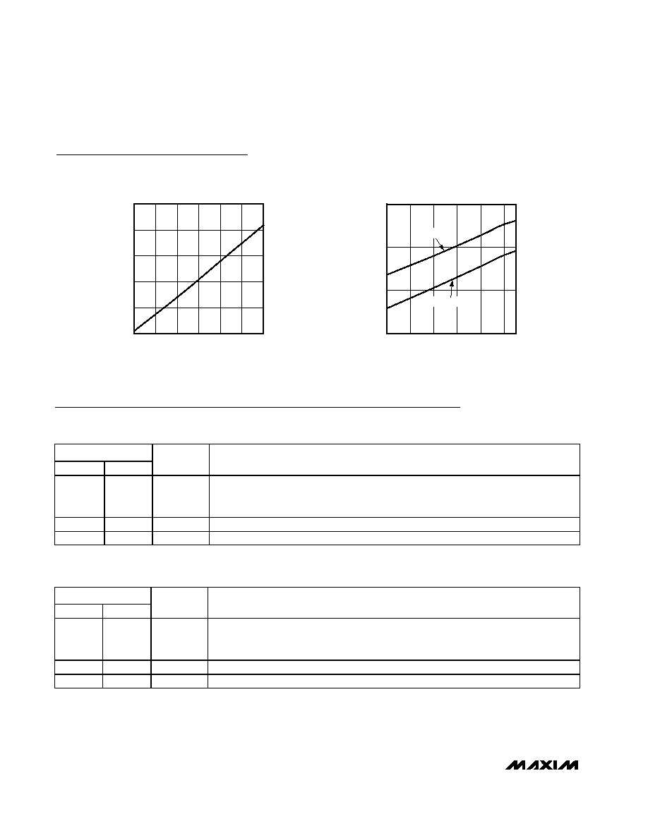
MAXIMUM TRANSIENT DURATION
vs. RESET THRESHOLD OVERDRIVE
20
10
MXD1810-13/15 toc05
RESET THRESHOLD OVERDRIVE, V
TH
- V
CC
(mV)
MAXIMUM TRANSIENT DURATION (
µ
s)
40
30
60
70
50
80
90
RESET OCCURS
ABOVE THIS LINE
0
40
120
80
160
200
0
6
3
9
12
15
OUTPUT VOLTAGE
vs. OUTPUT SINK CURRENT
MXD1810-13/15-18 toc06
OUTPUT CURRENT (mA)
OUTPUT VOLTAGE (mV)
Typical Operating Characteristics
(T
A
= +25∞C, unless otherwise noted.)
MXD1810≠MXD1813/MXD1815≠MXD1818
Low-Power µP Reset Circuits in 3-Pin
SC70/SOT23
4
_______________________________________________________________________________________
0
0.1
0.3
0.2
0.4
0.5
0
1.0
0.5
1.5
2.5
3.0
OUTPUT VOLTAGE
vs. OUTPUT SOURCE CURRENT
MXD1810-13/15-18 toc07
OUTPUT CURRENT (mA)
V
CC
- V
OUT
(V)
2.0
0.2
0.6
0.4
0.8
INPUT LOW VOLTAGE
vs. V
CC
AND TEMPERATURE
MXD1810-13/15 toc08
TEMPERATURE (
∞C)
INPUT LOW VOLTAGE (V)
-40
20
-10
50
80
110
V
CC
= +5.5V
V
CC
= +2.2V
Typical Operating Characteristics (continued)
(T
A
= +25∞C, unless otherwise noted.)
PIN
SC70
SOT23
NAME
FUNCTION
2
1
RESET
Push-Pull, Active-Low Reset Output. RESET changes from high to low when V
CC
drops
below the selected reset threshold. RESET remains low for the reset timeout period after
VCC exceeds the device reset threshold.
1
2
V
CC
Supply Voltage and Input for Reset Threshold Monitor
3
3
GND
Ground
MXD1810/MXD1815
PIN
SC70
SOT23
NAME
FUNCTION
2
1
RESET
Open-Drain, Active-Low Reset Output. RESET changes from high to low when V
CC
drops
below the selected reset threshold. RESET remains low for the reset timeout period after
V
CC
exceeds the device reset threshold. RESET has an internal 5.5k
pullup resistor.
1
2
V
CC
Supply Voltage and Input for Reset Threshold Monitor
3
3
GND
Ground
MXD1811/MXD1816
Pin Descriptions

Detailed Description
RESET/RESET Output
A microprocessor's (µP's) reset input starts the micro-
processor in a known state. The MXD1810≠MXD1813/
MXD1815≠MXD1818 µP supervisory circuits assert
reset to prevent code-execution errors during power-
up, power-down, and brownout conditions (Figure 4).
Whenever V
CC
falls below the reset threshold, the reset
output asserts. Once V
CC
exceeds the reset threshold,
an internal timer keeps the reset output asserted for the
specified reset timeout period (t
RP
). Reset is also trig-
gered by an externally initiated rising edge on the
RESET pin (MXD1813/MXD1818), following a low signal
of 1.5µs minimum duration.
Push-Button Reset (MXD1813/MXD1818)
Many µP-based products require push-button reset
capability (Figure 5), allowing the operator, a test tech-
nician, or external logic circuitry to initiate reset. On the
MXD1813/MXD1818, a logic-low on RESET held for
greater than 1.5µs asserts a reset. RESET deasserts
following a 100ms minimum reset timeout delay
(t
PBRST
). A manual reset input shorter than 1.5µs may
release RESET without the 100ms minimum reset time-
out delay. To facilitate use with mechanical switches,
the MXD1813/MXD1818 contain internal debouncing
circuitry. A debounced waveform is shown in Figure 6.
Applications Information
Interfacing to µPs with Bidirectional
Reset Pins
Since the RESET output on the MXD1811/MXD1816 is
open drain, these devices interface easily with µPs that
have bidirectional reset pins, such as the Motorola
68HC11. Connecting the µP supervisor's RESET output
directly to the microcontroller's (µC's) RESET pin allows
either device to assert reset (Figure 7). No external
pullup resistor is required, as it is contained within the
MXD1811/MXD1816.
Negative-Going V
CC
Transients
In addition to issuing a reset to the µP during power-up,
power-down, and brownout conditions, these devices
are relatively immune to short-duration, negative-going
V
CC
transients (glitches).
MXD1810≠MXD1813/MXD1815≠MXD1818
Low-Power µP Reset Circuits in 3-Pin
SC70/SOT23
_______________________________________________________________________________________
5
PIN
SC70
SOT23
NAME
FUNCTION
2
1
RESET
Push-Pull, Active-High Reset Output. RESET changes from low to high when V
CC
drops
below the selected reset threshold. RESET remains high for the reset timeout period after
V
CC
exceeds the device reset threshold.
1
2
V
CC
Supply Voltage and Input for Reset Threshold Monitor
3
3
GND
Ground
MXD1812/MXD1817
PIN
SC70
SOT23
NAME
FUNCTION
2
1
RESET
Open-Drain, Active-Low Reset Output with Manual Reset Detect. RESET changes from
high to low when V
CC
drops below the selected reset threshold, or RESET is externally
pulled low for at least 1.5µs. RESET remains low for the reset timeout period after V
CC
exceeds the device reset threshold or after the external manual reset is released. RESET
has an internal 5.5k
pullup resistor.
1
2
V
CC
Supply Voltage and Input for Reset Threshold Monitor
3
3
GND
Ground
MXD1813/MXD1818
Pin Descriptions (continued)
MXD1810≠MXD1813/MXD1815≠MXD1818
The Typical Operating Characteristics show the
Maximum Transient Duration vs. Reset Threshold
Overdrive for which reset pulses are not generated. The
graph shows the maximum pulse width that a negative-
going V
CC
transient may typically have without issuing a
reset signal. As the amplitude of the transient increases,
the maximum allowable pulse width decreases.
Ensuring a Valid Reset Output Down to
V
CC
= 0
When V
CC
falls below the minimum operating voltage,
push-pull structured reset sinking (or sourcing) capabil-
ities decrease dramatically. High-impedance CMOS-
logic inputs connected to the RESET/RESET pin can
drift to indeterminate voltages. This does not present a
problem in most cases, since most µPs and circuitry do
not operate at V
CC
below +1V. For MXD1810/
MXD1815 applications where RESET must be valid
down to V
CC
= 0, adding a pulldown resistor between
RESET and GND removes stray leakage currents, hold-
ing RESET low (Figure 8). The pulldown resistor value is
not critical; 100k
is large enough not to load RESET
and small enough to pull RESET low. For MXD1812/
Low-Power µP Reset Circuits in 3-Pin
SC70/SOT23
6
_______________________________________________________________________________________
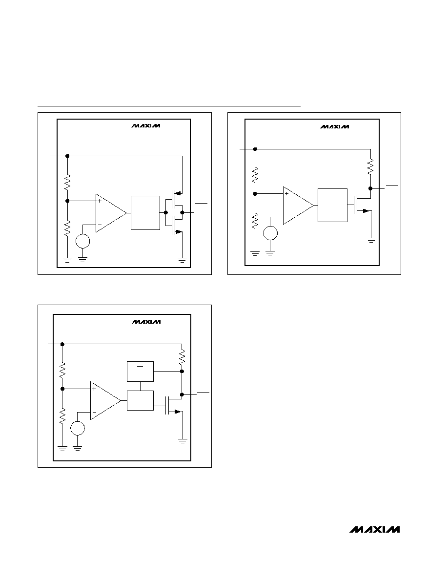
RESET
GENERATOR
V
REF
V
CC
RESET
OR
RESET
MXD1810
MXD1812
MXD1815
MXD1817
Figure 1. Functional Diagram, Push-Pull Output
RESET
GENERATOR
V
REF
V
CC
RESET
MXD1811
MXD1816
Figure 2. Functional Diagram, Open-Drain Active-Low Output
MR
MONITOR
V
REF
V
CC
RESET
MXD1813
MXD1818
RESET
GENERATOR
Figure 3. Functional Diagram, Open-Drain Active-Low Output
with Manual Reset Detection
Functional Diagram

MXD1817 applications where RESET must be valid to
V
CC
= 0, a 100k
pullup resistor between RESET and
V
CC
holds RESET high when V
CC
falls below the mini-
mum operating voltage (Figure 9).
The MXD1811/MXD1813/MXD1816/MXD1818 have
open-drain, active-low outputs with a pullup resistor
included internal to the devices. While using these
devices RESET will most likely not maintain an active
condition when the supply voltage drops below the
minimum V
CC
, but will drift to a nonactive level due to
the pullup resistor and the reduced sinking capability of
the open-drain output. Therefore, these devices are not
recommended for applications where the RESET pin is
required to be valid at V
CC
= 0.
MXD1810≠MXD1813/MXD1815≠MXD1818
Low-Power µP Reset Circuits in 3-Pin
SC70/SOT23
_______________________________________________________________________________________
7
V
TH
V
CC
t
RP
V
CC(MIN)
t
RP
RESET
RESET
Figure 4. Power-Up Reset Timing Diagram
MXD1813
MXD1818
V
CC
RESET
RESET
MANUAL
RESET
V
CC
GND
Figure 5. Push-Button Manual Reset
(OPEN)
V
CC
EXTERNAL
PUSH BUTTON
RESET
(OPEN)
(CLOSED)
t
PBRST
t
PBRST
SWITCH BOUNCE
Figure 6. Manual Reset Timing Diagram

MXD1810≠MXD1813/MXD1815≠MXD1818
Low-Power µP Reset Circuits in 3-Pin
SC70/SOT23
8
_______________________________________________________________________________________
MXD1811
MXD1816
GND
GND
V
CC
V
CC
V
CC
µP
RESET
RESET
Figure 7. Interfacing to Microprocessors with Bidirectional
Reset Pins
MXD1810
MXD1815
GND
*MXD1810/MXD1815 ONLY
GND
V
CC
V
CC
V
CC
µP
RESET
RESET
R
PULLDOWN
*
Figure 8. Ensuring Valid RESET Output Down to V
CC
= 0
(MXD1810/MXD1815 only)
MXD1812
MXD1817
GND
*MXD1812/MXD1817 ONLY
GND
V
CC
V
CC
V
CC
µP
RESET
RESET
R
PULLUP
*
Figure 9. Ensuring Valid RESET Output Down to V
CC
= 0
(MXD1812/MXD1817 only)
TOP MARK
PART
SOT23
SC70
MXD1810_R46
FZIV
AEK
MXD1810_R44
FZKD
AHU
MXD1810_R41
FZKC
AHT
MXD1811_R46
FZKF
AHW
MXD1811_R44
FZIW
AEL
MXD1811_R41
FZKE
AHV
MXD1812_R46
FZKH
AHY
MXD1812_R44
FZKG
AHX
MXD1812_R41
FZIX
AEM
MXD1813_R46
FZIY
AEN
MXD1813_R44
FZKJ
AIA
MXD1813_R41
FZKI
AHZ
MXD1815_R31
FZKN
AIE
MXD1815_R29
FZIZ
AEO
MXD1815_R26
FZKM
AID
MXD1815_R23
FZKL
AIC
MXD1815_R22
FZKK
AIB
MXD1816_R31
FZKR
AII
MXD1816_R29
FZKQ
AIH
MXD1816_R26
FZKP
AIG
MXD1816_R23
FZKO
AIF
MXD1816_R22
FZJA
AEP
MXD1817_R31
FZJB
AEQ
MXD1817_R29
FZKV
AIM
MXD1817_R26
FZKU
AIL
MXD1817_R23
FZKT
AIK
MXD1817_R22
FZKS
AIJ
MXD1818_R31
FZKY
AIP
MXD1818_R29
FZKX
AIO
MXD1818_R26
FZJC
AER
MXD1818_R23
FZKW
AIN
MXD1818_R22
FZJE
AEV
Table 1. Device Marking Codes
MXD1810≠MXD1813/MXD1815≠MXD1818
Low-Power µP Reset Circuits in 3-Pin
SC70/SOT23
_______________________________________________________________________________________
9
Selector Guide
PART
5V SYSTEMS
2.5V/3.0V/3.3V
SYSTEMS
PUSH-PULL
RESET
OPEN-DRAIN
RESET
PUSH-PULL
RESET
OPEN-DRAIN
RESET WITH
PUSH-
BUTTON
DETECT
MXD1810
--
--
--
--
MXD1811
--
--
--
--
MXD1812
--
--
--
--
MXD1813
--
--
--
--
MXD1815
--
--
--
--
MXD1816
--
--
--
--
MXD1817
--
--
--
--
MXD1818
--
--
--
--
Ordering Information (continued)
PART
TEMP. RANGE
PIN-PACKAGE
MXD1811UR_ _-T
-40
o
C to +105
o
C
3 SOT23-3
MXD1811XR_ _-T
-40
o
C to +105
o
C
3 SC70-3
MXD1812UR_ _-T
-40
o
C to +105
o
C
3 SOT23-3
MXD1812XR_ _-T
-40
o
C to +105
o
C
3 SC70-3
MXD1813UR_ _-T
-40
o
C to +105
o
C
3 SOT23-3
MXD1813XR_ _-T
-40
o
C to +105
o
C
3 SC70-3
MXD1815UR_ _-T
-40
o
C to +105
o
C
3 SOT23-3
MXD1815XR_ _-T
-40
o
C to +105
o
C
3 SC70-3
MXD1816UR_ _-T
-40
o
C to +105
o
C
3 SOT23-3
MXD1816XR_ _-T
-40
o
C to +105
o
C
3 SC70-3
MXD1817UR_ _-T
-40
o
C to +105
o
C
3 SOT23-3
MXD1817XR_ _-T
-40
o
C to +105
o
C
3 SC70-3
MXD1818UR_ _-T
-40
o
C to +105
o
C
3 SOT23-3
MXD1818XR_ _-T
-40
o
C to +105
o
C
3 SC70-3
Reset Threshold Table
PART
SUFFIX
(_ _)
TYP. RESET
THRESHOLD (V)
*
MXD1810≠MXD1813
46
4.62
MXD1810≠MXD1813
44
4.37
MXD1810≠MXD1813
41
4.12
MXD1815≠MXD1818
31
3.06
MXD1815≠MXD1818
29
2.88
MXD1815≠MXD1818
26
2.55
MXD1815≠MXD1818
23
2.31
MXD1815≠MXD1818
22
2.18
*Factory-trimmed reset thresholds are nominally ±1.5% at
room temperature.
Chip Information
TRANSISTOR COUNT: 709
PROCESS TECHNOLOGY: BiCMOS
The MXD1810≠MXD1813/MXD1815≠MXD1818 are available
with factory-set V
CC
reset thresholds from +2.18V to +3.06V
(MXD1815≠MXD1818) and +4.12V to +4.62V (MXD1810≠
MXD1813). Choose the desired reset-threshold suffix from the
Reset Threshold Table and insert it in place of the "_ _" follow-
ing "R" in the part number. All devices are available in tape-
and-reel only in 2500 unit increments. Other threshold voltages
may be available. Contact factory for availability.
MXD1810≠MXD1813/MXD1815≠MXD1818
Low-Power µP Reset Circuits in 3-Pin
SC70/SOT23
10
______________________________________________________________________________________
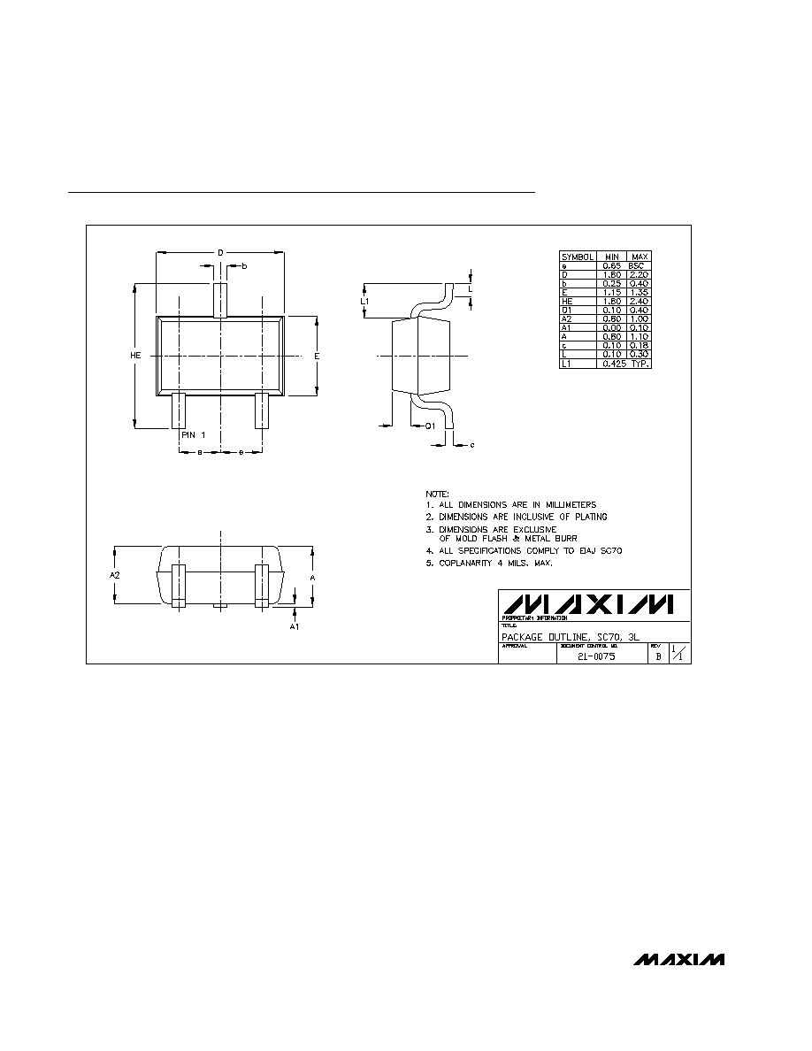
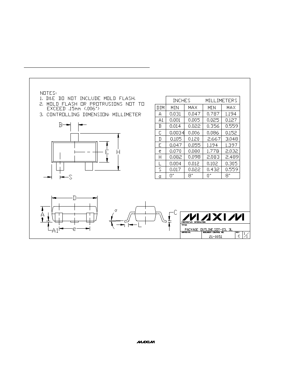
Package Information
SC70, 3L.EPS
MXD1810≠MXD1813/MXD1815≠MXD1818
Low-Power µP Reset Circuits in 3-Pin
SC70/SOT23
Maxim cannot assume responsibility for use of any circuitry other than circuitry entirely embodied in a Maxim product. No circuit patent licenses are
implied. Maxim reserves the right to change the circuitry and specifications without notice at any time.
Maxim Integrated Products, 120 San Gabriel Drive, Sunnyvale, CA 94086 408-737-7600 ____________________ 11
© 2001 Maxim Integrated Products
Printed USA
is a registered trademark of Maxim Integrated Products.
Package Information (continued)
SOTPO3L.EPS