 | –≠–ª–µ–∫—Ç—Ä–æ–Ω–Ω—ã–π –∫–æ–º–ø–æ–Ω–µ–Ω—Ç: MXL1014 | –°–∫–∞—á–∞—Ç—å:  PDF PDF  ZIP ZIP |
19-0133; Rev. 3; 4/98
General Description
The Maxim MXL1013 is a precision dual op amp that
upgrades the performance of popular devices such as the
MC1458/MC1558, LM158 and OP221. The Maxim
MXL1014 is a precision quad op amp that directly
upgrades designs in the industry-standard 14-pin DIP
configuration and has specifications similar to the
LT1013. The MXL1013 and MXL1014 are pin compati-
ble with industry standards such as the LT1013 and
LT1014.
Precision specifications include: 40µV offset voltage,
0.3µV/∞C drift (TCV
OS
), 117dB CMRR, and 120dB PSRR.
While supply current is typically only 350µA per amplifier,
the outputs can source and sink more than 20mA.
Both the MXL1013 and the MXL1014 can be operated
from a single +5V power supply. The input voltage
range includes ground and the outputs swing to within
a few millivolts of ground.
________________________Applications
Battery-Powered Precision Instrumentation
Strain-Gauge Signal Conditioners
Thermocouple Amplifiers
Instrumentation Amplifiers
4mA to 20mA Current-Loop Transmitters
Multiple-Limit Threshold Detection
Active Filters
Multiple Gain Blocks
____________________________Features
o
Single-Supply Operation
Input Voltage Range Extends to Ground
Output Swings to Ground while Sinking Current
o
150µV Max Offset Voltage
o
Low Drift: 2µV/∞C Max
o
0.8nA Max Offset Current
o
Guaranteed High Gain
5mA Load Current: 1.5 Million Min
17mA Load Current: 0.8 Million Min
o
500µA Max Supply Current per Amplifier
o
Low Voltage Noise: 0.1Hz to 10Hz, 0.55µV
p-p
o
Lower Current Noise than OP07: 0.07 pA/
Hz
Ordering Information
MXL1013/MXL1014
Dual/Quad Precision Op Amps
_________________________________________________________________ Maxim Integrated Products
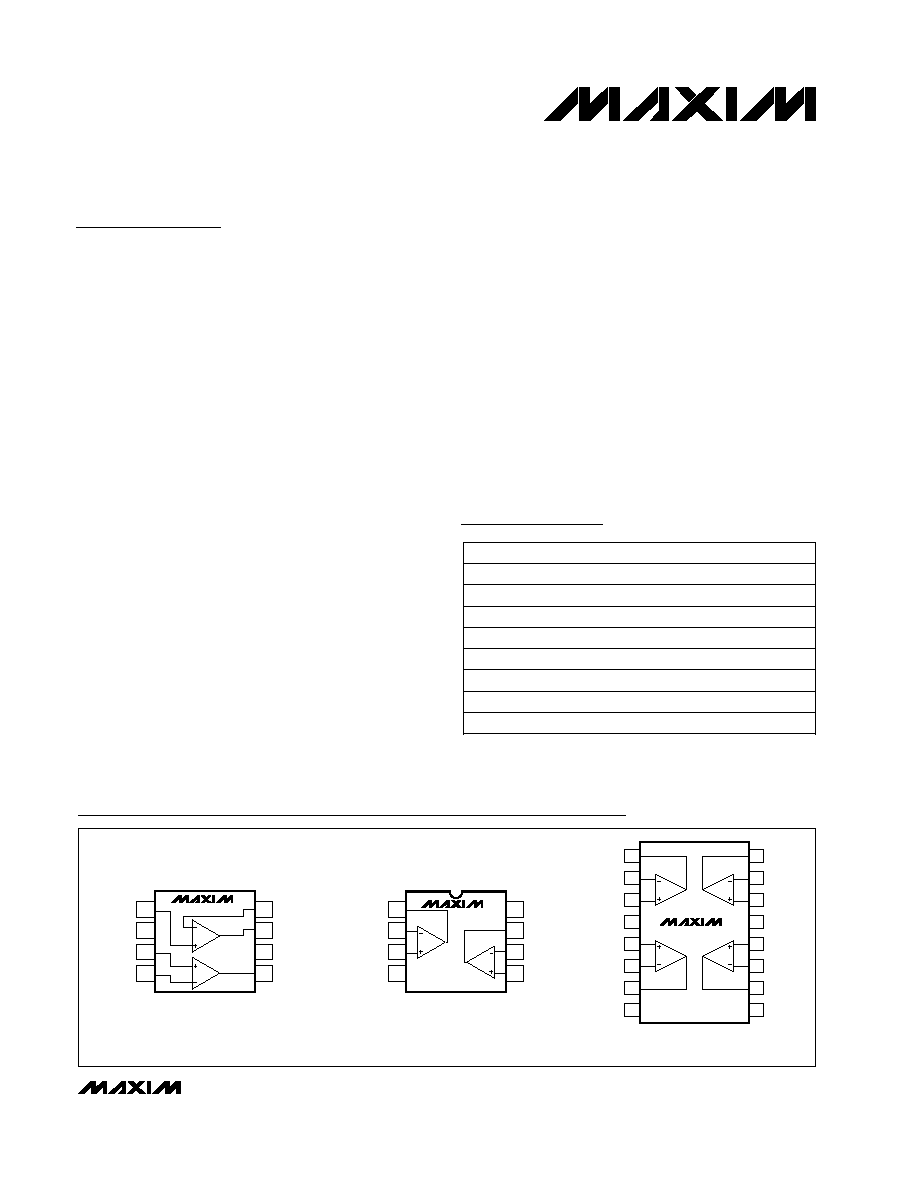
1
1
2
3
4
5
6
7
8
INA+
V-
INB+
INB-
INA-
OUTA
V+
OUTB
MXL1013
SO
A
B
1
2
3
4
5
6
7
8
OUTA+
INA-
INA+
V-
V+
OUTB
INB-
INB+
MXL1013
DIP
A
B
8
N.C.
N.C.
1
2
3
4
5
6
7
16
15
14
13
12
11
10
OUTA
INA-
INA+
V+
INB+
INB-
OUTB
OUTD
IND-
IND+
V-
INC+
INC-
OUTC
Wide SO
MXL1014
9
A
D
B
C
Pin Configurations
TOP VIEW
Pin Configurations continued on last page.
NOTE:
SO PIN CONFIGURATION DIFFERS
FROM DIP.
Dice*
0∞C to +70∞C
MXL1013DC/D
8 CERDIP**
-55∞C to +125∞C
MXL1013MJ8
-40∞C to +85∞C
MXL1013DS8
8 CERDIP**
-55∞C to +125∞C
MXL1013AMJ8
8 SO
MXL1013IS8
8 Plastic DIP
-40∞C to +85∞C
MXL1013IN8
8 SO
0∞C to +70∞C
8 Plastic DIP
0∞C to +70∞C
MXL1013DN8
8 Plastic DIP
0∞C to +70∞C
MXL1013
CN8
PIN-PACKAGE
TEMP. RANGE
PART
Ordering Information continued on last page.
*
Dice are specified at T
A
= +25∞C, D.C. parameters only.
**
Contact factory for availability and processing to MIL-STD-883.
For free samples & the latest literature: http://www.maxim-ic.com, or phone 1-800-998-8800.
For small orders, phone 1-800-835-8769.
MXL1013/MXL1014
ABSOLUTE MAXIMUM RATINGS
Supply Voltage.....................................................................±22V
Input Voltage ............................Equal to Positive Supply Voltage
........................5V Below Negative Supply Voltage
Output Short-Circuit Duration.....................................Continuous
Differential Input Voltage .....................................................±30V
Continuous Power Dissipation (T
A
= +70∞C)
8-Pin Plastic DIP (derate 9.09mW/∞C above +70∞C)......727mW
8-Pin SO (derate 5.88mW/∞C above +70∞C) ..................471mW
8-Pin CERDIP (derate 8.00mW/∞C above +70∞C) ..........640mW
14-Pin Plastic DIP (derate 10.00mW/∞C above +70∞C)..800mW
14-Pin CERDIP (derate 9.09mW/∞C above +70∞C) ........727mW
16-Pin Wide SO (derate 9.52mW/∞C above +70∞C).......762mW
Operating Temperature Ranges:
MXL1013/MXL1014C_ ........................................0∞C to +70∞C
MXL1013/MXL1014I_.......................................-40∞C to +85∞C
MXL1013/MXL1014AM_,M_ ..........................-55∞C to +125∞C
Storage Temperature Range .............................-65∞C to +150∞C
Lead Temperature (soldering, 10sec) .............................+300∞C
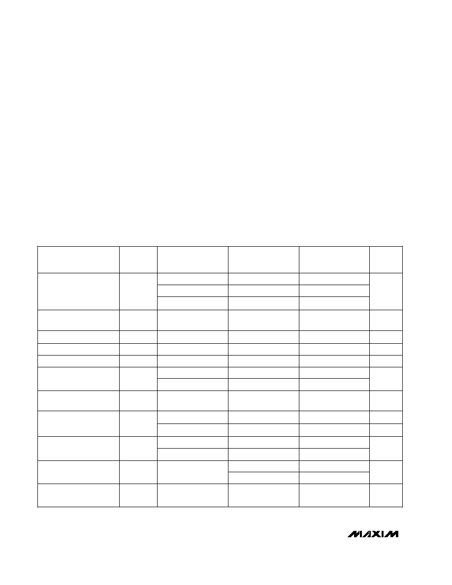
ELECTRICAL CHARACTERISTICS (Note 1)
(V
S
= ±15V, V
CM
= 0V, T
A
= +25∞C, unless otherwise noted.)
Dual/Quad Precision Op Amps
2
_______________________________________________________________________________________
Stresses beyond those listed under "Absolute Maximum Ratings" may cause permanent damage to the device. These are stress ratings only, and functional
operation of the device at these or any other conditions beyond those indicated in the operational sections of the specifications is not implied. Exposure to
absolute maximum rating conditions for extended periods may affect device reliability.
Input Resistance
(Note 2)
MXL1013AM
MXL1014AM
MIN
TYP
MAX
MXL1013C/D/I/M
MXL1014C/D/I/M
MIN
TYP
MAX
Common mode
Input Offset Voltage
V
OS
MXL1013
40
150
60
300
µV
0.4
0.5
µV/Mo.
Input Offset Current
I
OS
0.15
0.80
0.2
1.5
nA
Input Bias Current
I
B
12
20
15
30
nA
Input Noise Voltage
e
n
0.1Hz to 10Hz
0.55
µV
p-p
i
n
f
O
= 10Hz
0.07
0.07
pA/
Hz
100
400
PARAMETER
SYMBOL
CONDITIONS
UNITS
70
300
M
Large-Signal Voltage
Gain
A
VOL
V
O
= ±10V, R
L
= 2k
1.5
8.0
1.2
7.0
Input Voltage Range
+13.5
+13.8
+13.5
+13.8
V
Common-Mode Rejection
Ratio
CMRR
V
CM
= +13.5V, -15.0V
100
117
97
114
dB
MXL101_D/I
200
800
Input Noise-Voltage
Density
e
n
f
O
= 10Hz
24
24
nV/
Hz
f
O
= 1000Hz
MXL1014
50
180
22
22
5
4
G
-15.0
-15.3
-15.0
-15.3
V
O
= ±10V, R
L
= 600
0.8
2.5
0.5
2.0
V/µV
0.55
60
300
Long-Term Input Offset
Voltage Stability
Input Noise-Current
Density
Differential
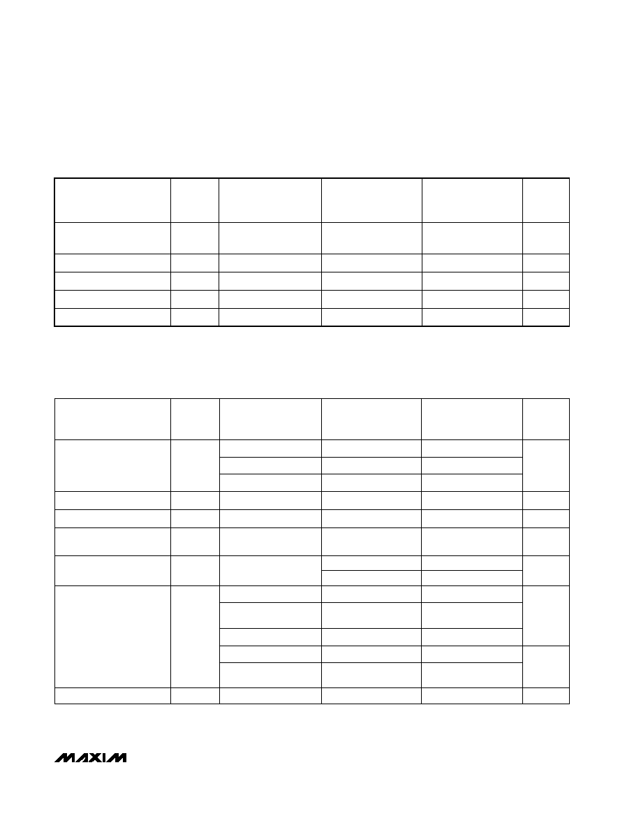
ELECTRICAL CHARACTERISTICS (continued) (Note 1)
(V
S
= ±15V, V
CM
= 0V, T
A
= +25∞C, unless otherwise noted.)
ELECTRICAL CHARACTERISTICS (Note 1)
(V
S
+ = +5V, V
S
- = 0V, V
OUT
= +1.4V, V
CM
= 0V, T
A
= +25∞C, unless otherwise noted.)
MXL1013/MXL1014
Dual/Quad Precision Op Amps
_______________________________________________________________________________________
3
Note 1:
When amplifier is sinking current at the output a minimum load of 1k
is recommended.
Note 2:
Guaranteed by design.
Channel Separation
MXL1013AM
MXL1014AM
MIN
TYP
MAX
MXL1013C/D/I/M
MXL1014C/D/I/M
MIN
TYP
MAX
V
O
= ±10V, R
L
= 2k
123
140
120
137
dB
Output Voltage Swing
V
OUT
R
L
= 2k
Power-Supply Rejection
Ratio
PSRR
V
S
= ±2V to ±18V
103
120
100
117
dB
±13
±14
V
Slew Rate
0.2
0.4
0.2
0.4
V/µs
Supply Current
I
S
Per amplifier
0.35
0.55
mA
PARAMETER
SYMBOL
CONDITIONS
UNITS
±12.5
±14
Input Bias Current
MXL1013AM
MXL1014AM
MIN
TYP
MAX
I
B
MXL1013C/D/I/M
MXL1014C/D/I/M
MIN
TYP
MAX
15
35
18
50
nA
Large-Signal Voltage
Gain
A
VOL
V
O
= 5mV to 4V,
R
L
=500
Input Offset Voltage
V
OS
MXL1013
60
250
90
450
Input Offset Current
I
OS
0.2
1.3
0.3
2.0
nA
1.0
1.0
V/µV
Input Voltage Range
+3.5
+3.8
+3.5
+3.8
V
Output Voltage Swing
V
OUT
Output low, no load
15
25
mV
Output low, 600
to
ground
PARAMETER
SYMBOL
CONDITIONS
UNITS
5
10
5
10
MXL1014
Output low, I
SINK
= 1mA
220
350
220
350
70
280
Output high, no load
4.0
4.4
4.0
4.4
Output high, 600
to
ground
3.4
4.0
3.4
4.0
Supply Current
I
S
Per amplifier
0.31
0.45
0.32
0.50
mA
90
450
0
-0.3
MXL101_D/I
250
950
µV
0
-0.3
0.35
0.50
15
25
V
MXL1013/MXL1014
Dual/Quad Precision Op Amps
4
_______________________________________________________________________________________
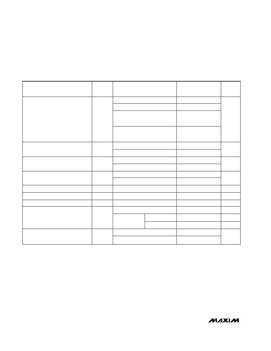
ELECTRICAL CHARACTERISTICS (Note 1)
(V
S
= ±15V, V
CM
= 0V, T
A
= -40∞C to +85∞C for MXL1013I and MXL1014I, T
A
= 0∞C to +70∞C for MXL1013C/D and MXL1014C/D,
unless otherwise noted.)
Power-Supply Rejection Ratio
PSRR
MXL1013C/D/I
MXL1014C/D/I
MIN
TYP
MAX
V
S
= ±2V to ±18V
Input Offset Voltage
V
OS
MXL101_C
80
400
µV
Input Bias Current
I
B
nA
V
S
= 5V, 0V; V
O
= 1.4V
MXL101_D/I:
V
S
= 5V, 0V; V
O
=1.4V
280
1200
Input Offset-Voltage Drift
TCV
OS
0.7
5.0
µV/∞C
PARAMETER
SYMBOL
CONDITIONS
UNITS
97
116
dB
Output low
Output Voltage Swing
V
OUT
R
L
= 2k
±12.0
±13.9
mV
Supply Current per Amplifier
I
S
V
S
= 5V, 0V, V
O
= 1.4V
0.37
0.60
mA
MXL101_C:
V
S
= 5V, 0V, V
O
= 1.4V
110
570
Input Offset Current
I
OS
nA
MXL101_D/I
230
1000
0.5
6.0
V
S
= 5V,0V,
R
L
= 600
6
13
24
90
Common-Mode Rejection Ratio
CMRR
V
CM
= +13.0V, -15.0V
94
113
dB
3.2
3.9
Output high
0.34
0.55
(Note 2)
0.4
2.5
V
S
= 5V, 0V; V
O
= 1.4V
MXL101_D/I (Note 2)
V
V
Large-Signal Voltage Gain
A
VOL
0.7
4.0
V/µV
0.3
2.8
16
38
V
O
= ±10V, R
L
= 2k
MXL1013/MXL1014
Dual/Quad Precision Op Amps
_______________________________________________________________________________________
5
ELECTRICAL CHARACTERISTICS (Note 1)
(V
S
= ±15V, V
CM
= 0V, T
A
= -55∞C to +125∞C, unless otherwise noted.)
Power-Supply
Rejection Ratio
MXL1013AM
MIN
TYP
MAX
PSRR
V
S
= ±2V to ±18V
Input Offset
Voltage
V
OS
80
300
µV
Input Bias
Current
I
B
15
30
nA
V
S
= 5V, 0V; V
O
= 1.4V
250
900
Input Offset-
Voltage Drift
TCV
OS
(Note 2)
0.4
2.0
µV/∞C
20
80
Large-Signal
Voltage Gain
A
VOL
V
O
= ±10V,
R
L
= 2k
0.5
2.0
V/µV
PARAMETER SYMBOL
CONDITIONS
UNITS
100
117
dB
Output low
Output
Voltage
Swing
V
OUT
R
L
= 2k
±12.0 ±13.8
V
Supply
Current
per Amplifier
I
S
0.38
0.60
mA
V
S
=
5V, 0V,
V
O
=
1.4V
120
450
Input Offset
Current
I
OS
0.3
2.5
nA
V
S
= 5V, 0V; V
O
= 1.4V
80
450
0.6
6.0
0.34
0.55
6
15
Common-
Mode
Rejection Ratio
CMRR
V
CM
= +13.0V, -14.9V
97
114
dB
V
S
=
5V,0V,
R
L
=
600
to
ground
3.2
3.8
Output high
V
V
S
= 5V, 0V; V
O
= 1.4V
Note 1:
When amplifier is sinking current at the output, a minimum load of 1k
is recommended.
Note 2:
Guaranteed by design.
Note 3:
This parameter is guaranteed by design and is not tested.
T
A
= -55∞C to
+100∞C (Note 3)
T
A
= +125∞C,
V
CM
= 0.1V
T
A
= +125∞C,
V
CM
= 0V
mV
MXL1014AM
MIN
TYP
MAX
90
350
15
30
300
960
0.4
2.0
25
90
0.4
2.0
100
117
±12.0 ±13.8
0.38
0.60
150
480
0.3
2.8
90
480
0.7
7.0
0.34
0.55
6
15
96
114
3.2
3.8
MXL1013M
MXL1014M
MIN
TYP
MAX
110
550
18
45
400
1500
0.5
2.5
28
120
0.25
2.0
97
116
±11.5 ±13.8
0.38
0.70
200
750
0.4
5.0
100
750
0.9
10.0
0.34
0.65
6
18
94
113
3.1
3.8