_______________General Description
The Maxim MXL1016 (10ns typ) and MXL1116 (12ns
typ) high-speed, complementary-output comparators
are designed specifically to interface directly to TTL
logic while operating from either a dual ±5V supply or a
single +5V supply.
The MXL1016/MXL1116 remain stable with the outputs
in the active region, which greatly reduces output insta-
bility common with slow-moving input signals. In addi-
tion, an output latch (LE) is provided.
For lower-power, higher-performance comparators, see
the MAX912/MAX913 dual/single comparator data
sheet. The MAX913 is an improved, plug-in replace-
ment for the MXL1016 and MXL1116, and the MAX912
is the dual equivalent to the MAX913.
________________________Applications
High-Speed A/D Converters
Zero-Crossing Detectors
Current Sense for Switching Regulators
High-Speed Sampling Circuits
High-Speed Triggers
Line Receivers
Extended Range V/F Converters
Fast Pulse Height/Width Discriminators
____________________________Features
o
Ultra Fast (10ns typ)
o
Single +5V or Dual ±5V Supply Operation
o
Input Common-Mode Extends to
Negative Supply (MXL1116)
o
Inputs Can Exceed the Positive Supply
Up to +15V (MXL1116) Without Damage
o
Complementary TTL Outputs
o
Low Offset Voltage:
1mV
o
No Minimum Input Slew-Rate Requirement
o
No Power-Supply Current Spiking
o
Output Latch
______________Ordering Information
MXL1016/MXL1116
Ultra-Fast Precision TTL Comparators
________________________________________________________________
Maxim Integrated Products
1
1
2
3
4
8
7
6
5
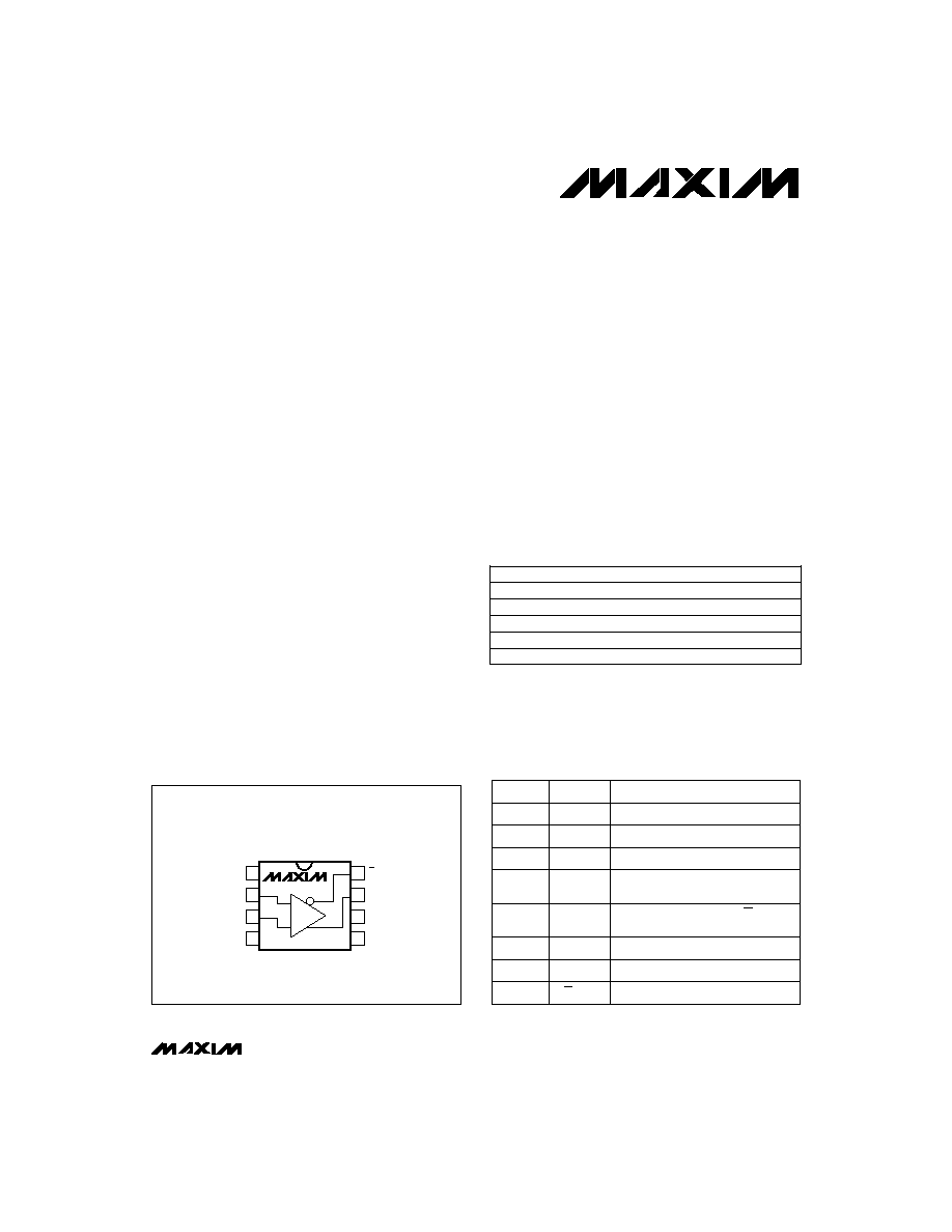
V+
IN+
IN≠
V≠
QOUT
QOUT
GND
LE
DIP/SO
MXL1016/MXL1116
+
-
__________________Pin Configuration
_____________________Pin Description
Call toll free 1-800-998-8800 for free samples or literature.
19-0138; Rev. 2; 4/95
PART
TEMP. RANGE
PIN-PACKAGE
MXL1016
CN8
0∞C to +70∞C
8 Plastic DIP
MXL1016CS8
0∞C to +70∞C
8 SO
MXL1016MJ8
≠55∞C to +125∞C
8 CERDIP
MXL1116
CN8
0∞C to +70∞C
8 Plastic DIP
MXL1116CS8
0∞C to +70∞C
8 SO
TOP VIEW
PIN
NAME
FUNCTION
1
V+
Positive Power Supply, +5V
2
IN+
Noninverting Input
3
IN-
Inverting Input
4
V-
Negative Power Supply, -5V for dual
supply or GND for single supply
5
LE
Latch Enable, QOUT and QOUT are
latched when LE is high
6
GND
Ground
7
QOUT
TTL Output
8
QOUT
Complementary TTL Output
MXL1016/MXL1116
2
_______________________________________________________________________________________
ABSOLUTE MAXIMUM RATINGS
Positive Supply Voltage............................................................7V
Negative Supply Voltage........................................................≠7V
Differential Input Voltage
MXL1016............................................................................±5V
MXL1116..........................................................................±15V
Input Voltage (either input)
MXL1016 ......................................................Equal to Supplies
MXL1116....................................................(V≠ ≠ 0.3V) to 15V
Latch Pin Voltage .............................................Equal to Supplies
Output Current (continuous).............................................±20mA
Continuous Power Dissipation (T
A
= +70∞C)
Plastic DIP (derate 9.09mW/∞C above +70∞C) ............727mW
SO (derate 5.88mW/∞C above +70∞C) .........................471mW
CERDIP (derate 8.00mW/∞C above +70∞C) .................640mW
Operating Temperature Ranges:
MXL1016C/MXL1116C .......................................0∞C to +70∞C
MXL1016MJ ..................................................≠55∞C to +125∞C
Storage Temperature Range ............................≠65∞C to +150∞C
Lead Temperature (soldering, 10sec) .............................+300∞C
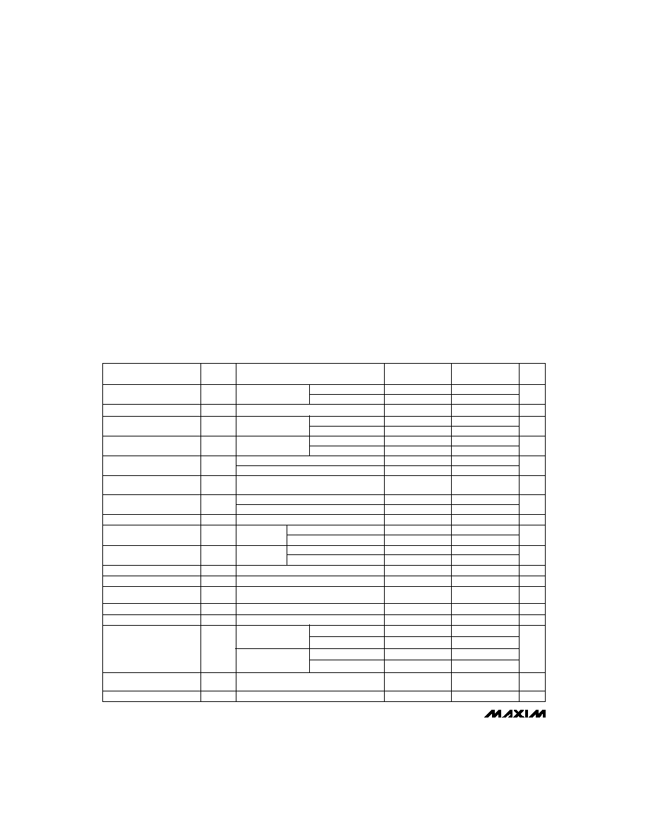
ELECTRICAL CHARACTERISTICS ≠ MXL1016
(V+ = 5V, V≠ = -5V, V
OUT
(Q) = 1.4V, V
LE
= 0V, T
A
= T
MIN
to T
MAX
, unless otherwise noted.)
Stresses beyond those listed under "Absolute Maximum Ratings" may cause permanent damage to the device. These are stress ratings only, and functional
operation of the device at these or any other conditions beyond those indicated in the operational sections of the specifications is not implied. Exposure to
absolute maximum rating conditions for extended periods may affect device reliability.
PARAMETER
MIN
CONDITIONS
MIN
TYP MAX
UNITS
Power-Supply
Rejection Ratio
TYP
Positive supply: 4.6V
V+
5.4V
60
75
dB
Small-Signal Voltage Gain
MAX
1V
V
OUT
2V, T
A
= +25∞C
1400 3000
V/V
Output High Voltage
MXL1016M
V+
4.6V
2.7
3.4
V
I
OUT
= 1mA
60
I
OUT
= 10mA
2.4
3.0
2.4
Positive Supply Current
75
25
35
mA
1400 3000
MXL1016C
2.7
3.4
Input Offset Voltage
(Note 1)
R
S
100
0.8
±2
mV
3.0
1.3
Input Offset-Voltage Drift
4
µV/∞C
25
1.3
13
35
Input Offset Current
(Note 1)
0.3
1
µA
Negative Supply Current
3
5
mA
Latch Pin High Input
Voltage
1.0
2.0
V
Latch Pin Low Input Voltage
±3
0.8
V
13
Input Bias Current
(Note 2)
4
Latch Pin Current
V
LE
= 0V
-500
µA
5
V
IN
= 100mV,
OD = 5mV
10
14
0.3
Propagation Delay
(Note 3)
V
IN
= 100mV,
OD = 20mV
9
12
ns
Differential Propagation
Delay (Note 3)
1
V
IN
= 100mV, OD = 5mV, T
A
= +25∞C
3
ns
Latch Setup Time
(Note 4)
2
ns
3
5
2.0
0.8
-500
10
14
9
12
3
2
Single 5V supply
+1.25
≠3.75
+3.5
80
96
SYMBOL
PSRR
A
V
+3.5
V
OH
+1.25
+3.5
Negative supply: ≠2V
V≠
≠7V
80
Input Voltage Range
≠3.75
+3.5
V
Common-Mode
Rejection Ratio
I+
≠3.75V
V
CM
3.5
80
96
dB
V
OS
V
OS
/
T
I
OS
I≠
V
IH
V
IL
I
IL
t
PD
t
PD
t
SU
100
V
CM
CMRR
3
3.5
10
µA
5
10
I
B
80
100
16
16
15
15
Output Low Voltage
0.3
0.5
V
I
SINK
= 4mA
I
SINK
= 10mA, T
A
= +25∞C
0.4
0.3
0.5
0.4
V
OL
Ultra-Fast Precision TTL Comparators
T
A
= +25∞C
T
A
= +25∞C
T
A
= +25∞C
T
A
= +25∞C
T
A
= +25∞C
MXL1016/MXL1116
Ultra-Fast Precision TTL Comparators
_________________________________________________________________________________________________
3
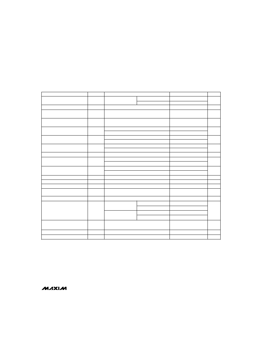
ELECTRICAL CHARACTERISTICS ≠ MXL1116
(V+ = 5V, V≠ = ≠5V, V
OUT
(Q) = 1.4V, V
LE
= 0V, T
A
= T
MIN
to T
MAX
, unless otherwise noted. Specifications for V
OS
, I
B
, CMRR and A
V
are valid for single-supply operation, V+ = 5V, V≠ = 0V.)
PARAMETER
MIN
CONDITIONS
UNITS
Power-Supply Rejection Ratio
TYP
Positive Supply: 4.6V
V+
5.4V
dB
Small-Signal Voltage Gain
MAX
1V
V
OUT
2V, T
A
= +25∞C
V/V
Output High Voltage
V
I
SOURCE
= 1mA
60
I
SOURCE
= 10mA
2.4
Positive Supply Current
75
mA
1400
3000
2.7
3.4
Input Offset Voltage
(Note 1)
R
S
100
mV
3.0
Input Offset-Voltage Drift
0.5
µV/∞C
27
2
38
Input Offset Current
(Note 1)
µA
Negative Supply Current
mA
Latch Pin High Input Voltage
1.0
V
Latch Pin Low Input Voltage
±3
V
10
20
Input Bias Current, Sourcing
(Note 2)
5
Latch Input Current
V
LE
= 0V
µA
V
IN
= 100mV,
OD = 5mV
Propagation Delay
(Note 3)
ns
Differential Propagation Delay
(Note 3)
V
IN
= 100mV, OD = 5mV, T
A
= +25∞C
ns
Latch Setup Time (Note 4)
ns
5
7
2.0
0.8
≠20
≠500
12
16
10
14
3
2
Single 5V supply
V≠
(V+ ≠ 2.5)
75
90
SYMBOL
PSRR
A
V
V
OH
0
2.5
Negative Supply: ≠7V
V≠
≠2V
Input Voltage Range
V
Common-Mode Rejection Ratio
I+
≠5V
V
CM
2.5V
dB
V
OS
V
OS
/
T
I
OS
I≠
V
IH
V
IL
I
IL
t
PD
t
PD
t
SU
V
CM
CMRR
3.5
µA
I
B
80
100
18
V
IN
= 100mV,
OD = 20mV
Output Low Voltage
V
I
SINK
= 4mA
I
SINK
= 10mA, T
A
= +25∞C
0.3
0.5
0.4
V
OL
0V
V
CM
2.5V, V
S
= +5V, 0V
65
90
16
Latch Hold Time (Note 4)
ns
2
t
H
Note 1:
Input offset voltage is defined as the average of the two input offset voltages, measured by forcing first one output, then the
other to 1.4V. Input offset current is defined in the same way.
Note 2:
Input bias current (I
B
) is defined as the average of the two input currents.
Note 3:
t
PD
and
t
PD
cannot be measured in automatic handling equipment with low values of overdrive. Correlation tests have
shown that t
PD
and
t
PD
limits shown can be guaranteed by design, if additional DC tests are performed to guarantee that
all internal bias conditions are correct. For low overdrive conditions, V
OS
is added to overdrive.
Note 4:
Input latch setup time, t
SU
, is the interval in which the input signal must be stable prior to asserting the latch signal. The hold
time, t
H
, is the interval after the latch is asserted in which the input signal must be stable.
T
A
= +25∞C
T
A
= +25∞C
T
A
= +25∞C
Maxim cannot assume responsibility for use of any circuitry other than circuitry entirely embodied in a Maxim product. No circuit patent licenses are
implied. Maxim reserves the right to change the circuitry and specifications without notice at any time.
4
_____________________________Maxim Integrated Products, 120 San Gabriel Drive, Sunnyvale, CA 94086 (408) 737-7600
© 1995 Maxim Integrated Products
Printed USA
is a registered trademark of Maxim Integrated Products.
MXL1016/MXL1116
Ultra-Fast Precision TTL Comparators
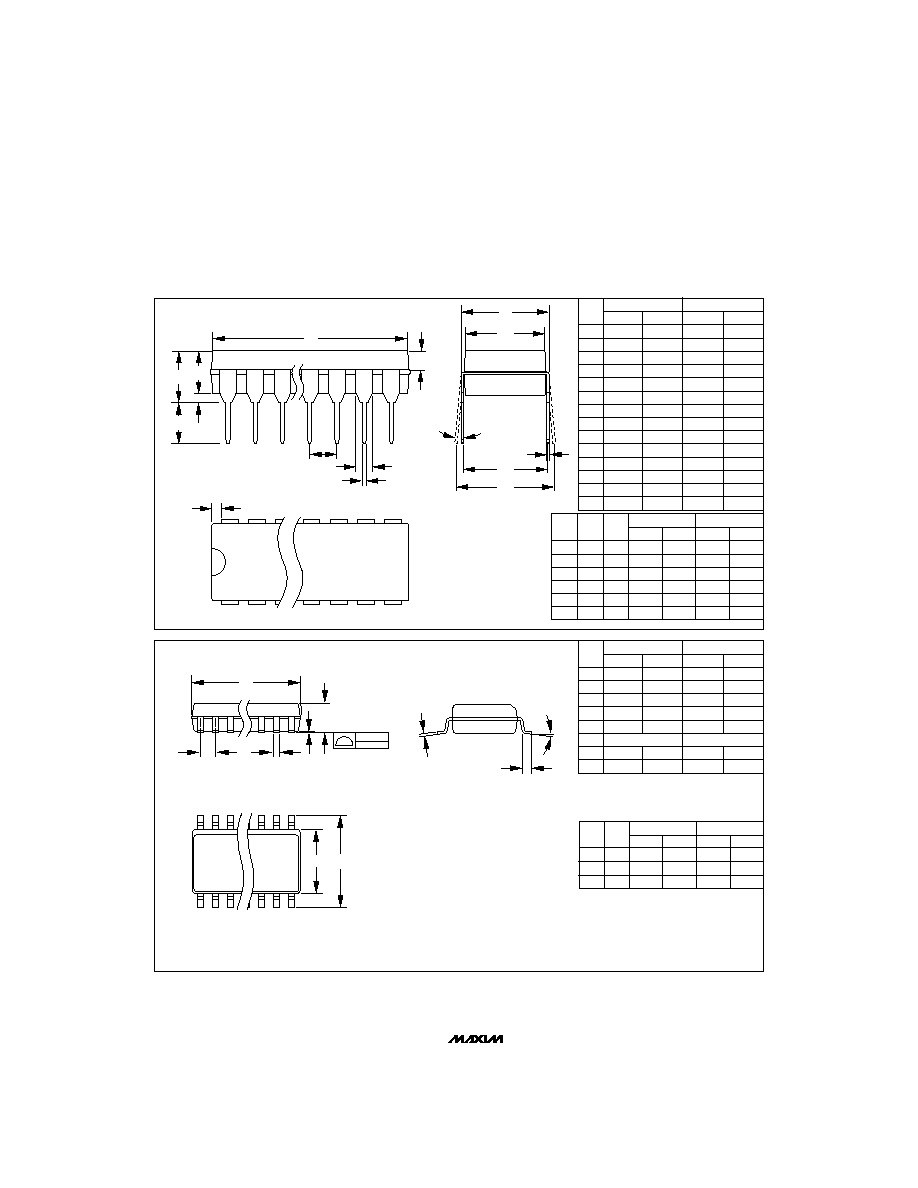
_______________________________________________________Package Information
DIM
A
A1
A2
A3
B
B1
C
D1
E
E1
e
eA
eB
L
MIN
≠
0.015
0.125
0.055
0.016
0.045
0.008
0.005
0.300
0.240
0.100
0.300
≠
0.115
MAX
0.200
≠
0.175
0.080
0.022
0.065
0.012
0.080
0.325
0.310
≠
≠
0.400
0.150
MIN
≠
0.38
3.18
1.40
0.41
1.14
0.20
0.13
7.62
6.10
2.54
7.62
≠
2.92
MAX
5.08
≠
4.45
2.03
0.56
1.65
0.30
2.03
8.26
7.87
≠
≠
10.16
3.81
INCHES
MILLIMETERS
Plastic DIP
PLASTIC
DUAL-IN-LINE
PACKAGE
(0.300 in.)
DIM
D
D
D
D
D
D
PKG.
P
P
P
P
P
N
MIN
0.348
0.735
0.745
0.885
1.015
1.14
MAX
0.390
0.765
0.765
0.915
1.045
1.265
MIN
8.84
18.67
18.92
22.48
25.78
28.96
MAX
9.91
19.43
19.43
23.24
26.54
32.13
INCHES
MILLIMETERS
PINS
8
14
16
18
20
24
C
A
A2
E1
D
E
eA
eB
A3
B1
B
0∞ - 15∞
A1
L
D1
e
21-0043A
DIM
A
A1
B
C
E
e
H
L
MIN
0.053
0.004
0.014
0.007
0.150
0.228
0.016
MAX
0.069
0.010
0.019
0.010
0.157
0.244
0.050
MIN
1.35
0.10
0.35
0.19
3.80
5.80
0.40
MAX
1.75
0.25
0.49
0.25
4.00
6.20
1.27
INCHES
MILLIMETERS
21-0041A
Narrow SO
SMALL-OUTLINE
PACKAGE
(0.150 in.)
DIM
D
D
D
MIN
0.189
0.337
0.386
MAX
0.197
0.344
0.394
MIN
4.80
8.55
9.80
MAX
5.00
8.75
10.00
INCHES
MILLIMETERS
PINS
8
14
16
1.27
0.050
L
0∞-8∞
H
E
D
e
A
A1
C
0.101mm
0.004in.
B