General Description
The MAX3535E/MXL1535E isolated RS-485/RS-422 full-
duplex transceivers provide 2500V
RMS
of galvanic isola-
tion between the RS-485/RS-422 side and the processor
or control logic side. These devices allow fast,
1000kbps communication across an isolation barrier
when the common-mode voltages (i.e., the ground
potentials) on either side of the barrier are subject to
large differences. Isolation is achieved through integrat-
ed high-voltage capacitors. The MAX3535E/MXL1535E
also feature a 420kHz transformer driver that allows
power transfer to the RS-485 side using an external
transformer.
The MAX3535E/MXL1535E include one differential driver,
one receiver, and internal circuitry to send the RS-485
signals and control signals across the isolation barrier
(including the isolation capacitors). The MAX3535E/
MXL1535E RS-485 receivers are 1/8 unit load, allowing
up to 256 devices on the same bus.
The MAX3535E/MXL1535E feature true fail-safe circuitry.
The driver outputs and the receiver inputs are protected
from ±15kV electrostatic discharge (ESD) on the inter-
face side, as specified in the Human Body Model (HBM).
The MAX3535E/MXL1535E feature driver slew-rate
select that minimizes electromagnetic interference (EMI)
and reduces reflections. The driver outputs are short-cir-
cuit and overvoltage protected. Other features are hot-
swap capability and isolation-barrier fault detection.
The MAX3535E operates with a single +3V to +5.5V
power supply. The improved secondary supply range of
the MAX3535E allows the use of step-down transformers
for +5V operation, resulting in considerable power sav-
ings. The MXL1535E operates with a single +4.5V to
+5.5V power supply. The MXL1535E is a function-/pin-
compatible improvement of the LTC1535. The
MAX3535E/MXL1535E are available over the commer-
cial 0∞C to +70∞C and extended -40∞C to +85∞C temper-
ature ranges.
Applications
Isolated RS-485 Systems
Systems with Large Common-Mode Voltages
Industrial-Control Local Area Networks
Telecommunications Systems
Features
2500V
RMS
RS-485 Bus Isolation Using On-Chip
High-Voltage Capacitors
1000kbps Full-Duplex RS-485/RS-422
Communication
+3V to +5.5V Power-Supply Voltage Range
(MAX3535E)
+4.5V to +5.5V Power-Supply Voltage Range
(MXL1535E)
1/8 Unit Receiver Load, Allowing 256 Devices on
Bus
±15kV ESD Protection Using HBM
Pin-Selectable Slew-Rate Limiting Controls EMI
Hot-Swap-Protected Driver-Enable Input
Undervoltage Lockout
Isolation-Barrier Fault Detection
Short-Circuit Protected
Thermal Shutdown
Open-Line and Shorted-Line Fail-Safe Receiver
Inputs
MAX3535E/MXL1535E
+3V to +5V, 2500V
RMS
Isolated RS-485/RS-422
Transceivers with ±15kV ESD Protection
________________________________________________________________ Maxim Integrated Products
1
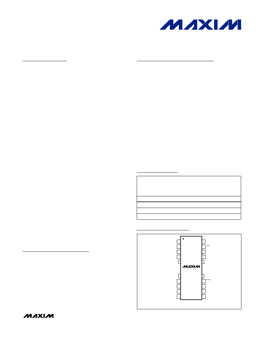
28
27
26
25
18
17
16
15
1
2
3
4
11
12
13
14
RO1
RE
DE
DI
B
SLO
RO2
A
V
CC2
PINS 5≠10 and 19≠24 ARE REMOVED FROM THE PACKAGE
Y
Z
GND2
GND1
ST2
ST1
V
CC1
WIDE SO
TOP VIEW
MAX3535E
MXL1535E
PART
TEMP RANGE
PIN-
PACKAGE
POWER-
SUPPLY
RANGE
(V)
MAX3535ECWI
0∞C to +70∞C
28 Wi d e S O
+ 3.0 to + 5.5
MAX3535EEWI
-40∞C to +85∞C
28 Wi d e S O
+ 3.0 to + 5.5
MXL1535ECWI
0∞C to +70∞C
28 Wi d e S O
+ 4.5 to + 5.5
MXL1535EEWI
-40∞C to +85∞C
28 Wi d e S O
+ 4.5 to + 5.5
Pin Configuration
Ordering Information
19-3270; Rev 0; 4/04
For pricing, delivery, and ordering information, please contact Maxim/Dallas Direct! at
1-888-629-4642, or visit Maxim's website at www.maxim-ic.com.
Typical Application Circuit appears at end of data sheet.
MAX3535E/MXL1535E
+3V to +5V, 2500V
RMS
Isolated RS-485/RS-422
Transceivers with ±15kV ESD Protection
2
_______________________________________________________________________________________
ABSOLUTE MAXIMUM RATINGS
DC ELECTRICAL CHARACTERISTICS TABLE (MAX3535E)
(V
CC1
= +3.0V to +5.5V, V
CC2
= +3.13V to +7.5V, T
A
= -40∞C to +85∞C, unless otherwise noted. Typical values are at V
CC1
= +3.3V,
V
CC2
= +5V, T
A
= +25∞C.)
Stresses beyond those listed under "Absolute Maximum Ratings" may cause permanent damage to the device. These are stress ratings only, and functional
operation of the device at these or any other conditions beyond those indicated in the operational sections of the specifications is not implied. Exposure to
absolute maximum rating conditions for extended periods may affect device reliability.
Logic Side--All Voltages Referenced to GND1.
V
CC1
.........................................................................-0.3V to +6V
RE, DE, DI.................................................................-0.3V to +6V
RO1, ST1, ST2 ..........................................-0.3V to (V
CC1
+ 0.3V)
Isolated Side--All Voltages Referenced to GND2.
V
CC2
.........................................................................-0.3V to +8V
SLO...........................................................-0.3V to (V
CC2
+ 0.3V)
A, B ......................................................................................±14V
RO2 .....................-0.3V to the lower of (V
CC2
+ 0.3V) and +3.4V
Y, Z ............................................................................-8V to +13V
Digital Outputs Maximum Current
RO1, RO2 .....................................................................±20mA
Y, Z Maximum Current .............................Short-Circuit Protected
ST1, ST2 Maximum Current............................................±300mA
Continuous Power Dissipation (T
A
= +70∞C)
28-Pin Wide SO
(derate 9.5mW/∞C above +70∞C) .................................750mW
Operating Temperature Range
MXL1535ECWI, MAX3535ECWI .........................0∞C to +70∞C
MXL1535EEWI, MAX3535EEWI .......................-40∞C to +85∞C
Junction Temperature ......................................................+150∞C
Storage Temperature Range .............................-65∞C to +150∞C
Lead Temperature (soldering, 10s) .................................+300∞C
PARAMETER
SYMBOL
CONDITIONS
MIN
TYP
MAX
UNITS
LOGIC-SIDE SUPPLY (V
CC1
, GND1)
Logic-Side Supply Voltage
V
CC1
3.0
5.5
V
Logic-Side Supply Current
I
CC1
Transformer not driven, ST1 and ST2
unconnected, RE = low, DE = high,
f
DATA
= 0, RO1 = no load
5.9
13
mA
V
CC1
Undervoltage-Lockout
Falling Trip
V
UVL1
2.53
2.69
2.85
V
V
CC1
Undervoltage-Lockout
Rising Trip
V
UVH1
2.63
2.80
2.97
V
LOGIC INPUTS (DI, DE,
RE)
Input High Voltage, DE, DI, RE
V
IH
V
IH
is measured with respect to GND1
2.0
V
Input Low Voltage, DE, DI, RE
V
IL
V
IL
is measured with respect to GND1
0.8
V
Logic-Side Input Current, DE, DI
I
INC
±2
µA
LOGIC OUTPUTS (RO1,
RE)
I
SOURCE
= 4mA, V
CC1
= +4.5V
3.7
Receiver-Output High Voltage
(RO1)
V
RO1H
I
SOURCE
= 4mA, V
CC1
= +3V
2.4
V
I
SINK
= 4mA, V
CC1
= +4.5V
0.4
Receiver-Output Low Voltage
(RO1)
V
RO1L
I
SINK
= 4mA, V
CC1
= +3V
0.4
V
Receiver-Output (RO1) Leakage
Current
I
OZR
RE = high, V
CC1
= +5.5V,
0
V
RO1
V
CC1
±1
µA
RE Low Output Current for Fault
Detect
I
OL
RE = +0.4V, fault not asserted
40
60
80
µA
MAX3535E/MXL1535E
+3V to +5V, 2500V
RMS
Isolated RS-485/RS-422
Transceivers with ±15kV ESD Protection
_______________________________________________________________________________________
3
DC ELECTRICAL CHARACTERISTICS TABLE (MAX3535E) (continued)
(V
CC1
= +3.0V to +5.5V, V
CC2
= +3.13V to +7.5V, T
A
= -40∞C to +85∞C, unless otherwise noted. Typical values are at V
CC1
= +3.3V,
V
CC2
= +5V, T
A
= +25∞C.)
PARAMETER
SYMBOL
CONDITIONS
MIN
TYP
MAX
UNITS
RE High Output Current for Fault
Detect
I
OH
RE = V
CC1
- 0.5V, fault asserted
-140
-100
-60
µA
TRANSFORMER DRIVER (ST1, ST2)
DC-Converter Switching
Frequency (ST1, ST2)
f
SW
ST1, ST2, not loaded
290
460
590
kHz
V
CC1
= +4.5V, Figure 13
1.6
2.6
DC-Converter Total Impedance
R
OH
+ R
OL
(ST1, ST2)
R
OHL
V
CC1
= +3V, Figure 13
1.8
2.9
ST1, ST2 Duty Cycle
ST1, ST2, not loaded
44
50
56
%
ISOLATED-SIDE SUPPLY (V
CC2
, GND2)
Isolated-Side Supply Voltage
V
CC2
3.13
7.50
V
R
L
= 27
56
70
Isolated-Side Supply Current
I
CC2
f
DATA
= 0, SLO floating,
RO2 = no load,
A, B floating, Figure 1
R
L
=
10
16
mA
V
CC2
Undervoltage-Lockout
Falling Trip
V
UVL2
2.68
2.85
3.02
V
V
CC2
Undervoltage-Lockout
Rising Trip
V
UVH2
2.77
2.95
3.13
V
DRIVER OUTPUTS (Y, Z)
Driver-Output High Voltage
V
DOH
No load, V
DOH
is measured with respect to
GND2
4
V
R
L
= 50
(RS-422), V
CC2
= +3.13V,
Figure 1
2.0
2.35
Differential Driver Output
V
OD
R
L
= 27
(RS-485), V
CC2
= +3.13V,
Figure 1
1.5
1.95
V
Driver Common-Mode Output
Voltage
V
OC
R
L
= 27
or 50, V
OC
is measured with
respect to GND2, Figure 1
1.0
3.0
V
Change in Magnitude of Driver
Differential Output Voltage for
Complementary Output States
V
OD
R
L
= 27
or 50, Figure 1
±0.2
V
Change in Magnitude of Driver
Common-Mode Output Voltage
for Complementary Output States
V
OC
R
L
= 27
or 50, Figure 1
±0.2
V
Driver enabled (DE =1 )
DI = high, V
Y
> -7V
DI = low, V
Z
> -7V
-250
Driver Short-Circuit Output
Current
I
OSD
Driver enabled (DE =1 )
DI = high, V
Z
< +12V
DI = low, V
Y
< +12V
+250
mA
MAX3535E/MXL1535E
+3V to +5V, 2500V
RMS
Isolated RS-485/RS-422
Transceivers with ±15kV ESD Protection
4
_______________________________________________________________________________________
DC ELECTRICAL CHARACTERISTICS TABLE (MAX3535E) (continued)
(V
CC1
= +3.0V to +5.5V, V
CC2
= +3.13V to +7.5V, T
A
= -40∞C to +85∞C, unless otherwise noted. Typical values are at T
A
= +25∞C,
V
CC1
= +3.3V, V
CC2
= +5V).
PARAMETER
SYMBOL
CONDITIONS
MIN
TYP
MAX
UNITS
DI = high
-7V < V
Y
< min[(V
CC2
- 1V) +2V]
DI = low
-7V < V
Z
< min[(V
CC2
- 1V) +2V]
-25
DI = high
+1V < V
Z
< +12V
Driver Short-Circuit Foldback
Output Current
I
OSFD
Driver
enabled
(DE =1)
DI = low
+1V < V
Y
< +12V
+25
µA
SLEW-RATE SELECT (
SLO)
Input High Voltage SLO
V
IHS
V
IHS
is measured with respect to GND2
3.0
V
Input Low Voltage SLO
V
ILS
V
ILS
is measured with respect to GND2
1.0
V
SLO Pullup Resistor
R
SLO
V
SLO
= +3V
100
k
RECEIVER INPUTS (A, B)
V
A
or V
B
= +12V
+125
Receiver Input Current
I
AB
V
A
or V
B
= -7V
-100
µA
Receiver Differential Threshold
Voltage
V
TH
-7V
V
CM
+12V
-200
-90
-10
mV
-7V
V
CM
+12V, T
A
= 0
∞C to +70∞C
10
30
70
Receiver-Input Hysteresis
V
TH
-7v
V
CM
+12V, T
A
= -40
∞C to +85∞C
5
30
70
mV
Receiver-Input Resistance
R
IN
-7V
V
CM
+12V (Note 1)
96
200
k
Receiver-Input Open Circuit
Voltage
V
OAB
2.6
V
RECEIVER OUTPUT (RO2)
Receiver-Output (RO2) High
Voltage
V
RO2H
I
SOURCE
= 4mA, V
CC2
= +3.13V
2.4
V
Receiver-Output (RO2) Low
Voltage
V
RO2L
I
SINK
= 4mA, V
CC2
= +3.13V
0.4
V
ISOLATION
60s
2500
Isolation Voltage (Notes 2, 3)
V
ISO
1s
3000
V
RMS
Isolation Resistance
R
ISO
T
A
= +25
∞C, V
ISO
= 50V (Note 3)
100
10,000
M
Isolation Capacitance
C
ISO
T
A
= +25
∞C
2
pF
ESD Protection
Human Body Model (A, B, Y, Z)
±15
kV
MAX3535E/MXL1535E
+3V to +5V, 2500V
RMS
Isolated RS-485/RS-422
Transceivers with ±15kV ESD Protection
_______________________________________________________________________________________
5
SWITCHING ELECTRICAL CHARACTERISTICS (MAX3535E)
(V
CC1
= +3.0V to +5.5V, V
CC2
= +3.13V to +7.5V, R
L
= 27
, C
L
= 50pF, T
A
= -40∞C to +85∞C, unless otherwise noted. Typical values
are at V
CC1
= +3.3V, V
CC2
= +5V, T
A
= +25∞C.)
PARAMETER
SYMBOL
CONDITIONS
MIN
TYP
MAX
UNITS
Data Sample Jitter
t
J
Figure 6
220
285
ns
Maximum Data Rate
f
DATA
t
J
= 25% of data cell, receiver and driver,
SLO = high (Note 4)
877
1136
kbps
SLO = high, Figure 5
250
450
Self-Oscillating Frequency
f
SOS
SLO = low, Figure 5
200
375
kHz
SLO = high, Figures 2, 6
490
855
Driver-Differential Output Delay
Time
t
DD
SLO = low, Figures 2, 6
850
1560
ns
SLO = high, Figures 2, 6
30
100
Driver-Differential Output
Transition Time
t
TD
SLO = low, Figures 2, 6
120
220
1000
ns
Driver-Output Enable Time
t
PZL
, t
PZH
SLO = high, DI = high or low,
Figures 3, 7
730
1400
ns
Driver-Output Disable Time
t
PHZ
, t
PLZ
SLO = high, DI = high or low,
Figures 3, 7
720
1300
ns
Receiver-Propagation Delay Time
to RO1
t
PLH1
,
t
PHL1
Figures 4, 8
440
855
ns
Receiver-Propagation Delay Time
to RO2
t
PLH2
,
t
PHL2
Figures 4, 8
40
ns
RO1, RO2 Rise or Fall Time
t
R
, t
F
Figures 4, 8
40
ns
Receiver-Output Enable Time
RO1
t
ZL
,t
ZH
Figures 4, 9
30
ns
Receiver-Output Disable Time
RO1
t
LZ
,t
HZ
Figures 4, 9
30
ns
Initial Startup Time (from Internal
Communication Fault)
(Note 5)
1200
ns
Internal Communication Timeout
Fault Time
(Note 5)
1200
ns
MAX3535E/MXL1535E
+3V to +5V, 2500V
RMS
Isolated RS-485/RS-422
Transceivers with ±15kV ESD Protection
6
_______________________________________________________________________________________
ELECTRICAL CHARACTERISTICS (MXL1535E)
(V
CC1
= +4.5V to +5.5V, V
CC2
= +4.5V to +7.5V, T
A
= -40∞C to +85∞C, unless otherwise noted. Typical values are at V
CC1
= +5V,
V
CC2
= +5V, T
A
= +25∞C.)
PARAMETER
SYMBOL
CONDITIONS
MIN
TYP
MAX
UNITS
Logic-Side Supply Voltage
V
CC1
4.5
5.5
V
Isolated-Side Supply Voltage
V
CC2
4.5
7.5
V
Logic-Side Supply Current
I
CC1
Transformer not driven, ST1 and ST2
unconnected, RE = low, DE = high,
f
DATA
= 0, RO1 = no load
5.9
13
mA
R
L
= 27
56
70
Isolated-Side Supply Current
I
CC2
f
DATA
= 0, SLO floating,
RO2 = no load, A, B
floating, Figure 1
R
L
=
10
16
mA
R
L
= 50
(RS-422), V
CC2
= +4.5V, Figure 1
2.0
3.0
Differential Driver Output
V
OD
R
L
= 27
(RS-485), V
CC2
= +4.5V, Figure 1
1.5
2.5
V
Driver Output High Voltage
V
DOH
No load, V
DOH
is measured with respect to
GND2
5.0
V
Driver Common-Mode Output
Voltage
V
OC
R
L
= 27
or 50, V
OC
is measured with
respect to GND2, Figure 1
1.0
3.0
V
Change in Magnitude of Driver
Differential Output Voltage for
Complementary Output States
V
OD
R
L
= 27
or 50, Figure 1
±0.2
V
Change in Magnitude of Driver
Common-Mode Output Voltage
for Complementary Output States
V
OC
R
L
= 27
or 50, Figure 1
±0.2
V
Driver enabled (DE =1)
DI = high, V
Y
> -7V
DI = low, V
Z
> -7V
-250
Driver Short-Circuit Output
Current
I
OSD
Driver enabled (DE =1)
DI = high, V
Z
< +12V
DI = low, V
Y
< + 12V
+250
mA
Driver enabled (DE =1)
DI = high
-7V < V
Y
< min[(V
CC2
- 1V) +2V]
DI = low
-7V < V
Z
< min[(V
CC2
- 1V) +2V]
-25
Driver Short-Circuit Foldback
Output Current
I
OSFD
Driver enabled (DE =1)
DI = high
+1V < V
Z
< +12V
DI = low
+1V < V
Y
< +12V
+25
mA
MAX3535E/MXL1535E
+3V to +5V, 2500V
RMS
Isolated RS-485/RS-422
Transceivers with ±15kV ESD Protection
_______________________________________________________________________________________
7
ELECTRICAL CHARACTERISTICS (MXL1535E) (continued)
(V
CC1
= +4.5V to +5.5V, V
CC2
= +4.5V to +7.5V, T
A
= -40∞C to +85∞C, unless otherwise noted. Typical values are at V
CC1
= +5V,
V
CC2
= +5V, T
A
= +25∞C.)
PARAMETER
SYMBOL
CONDITIONS
MIN
TYP
MAX
UNITS
Input High Voltage, DE, DI, RE
V
IH
V
IH
is measured with respect to GND1
2.0
1.45
V
Input High Voltage, SLO
V
IHS
V
IHS
is measured with respect to GND2
4.0
2.1
V
Input Low Voltage, DE, DI, RE
V
IL
V
IL
is measured with respect to GND1
1.45
0.8
V
Input Low Voltage, SLO
V
ILS
V
ILS
is measured with respect to GND2
2.1
1.0
V
Logic-Side Input Current, DE, DI
I
INC
±2
µA
V
A
or V
B
= +12V
+0.25
Receiver Input Current
I
AB
V
A
or V
B
= -7V
-0.20
mA
Receiver Differential Threshold
Voltage
V
TH
-7V
V
CM
+12V
-200
-90
-10
mV
-7V
V
CM
+12V, T
A
= 0∞C to +70∞C
10
30
70
Receiver-Input Hysteresis
V
TH
-7V
V
CM
+12V, T
A
= -40∞C to +85∞C
5
30
70
mV
Receiver-Input Resistance
R
IN
-7V
V
CM
+12V (Note 1)
96
140
200
k
Receiver-Input Open-Circuit
Voltage
V
OAB
2.6
V
Receiver-Output High Voltage
(RO1)
V
RO1H
I
SOURCE
= 4mA, V
CC1
= +4.5V
3.7
4.3
V
Receiver-Output Low Voltage
(RO1)
V
RO1L
I
SINK
= 4mA, V
CC1
= +4.5V
0.4
0.8
V
Driver-Output Leakage Current
I
OZ
DE = low
-7V < V
Y
< +12V, -7V < V
Z
< +12V
±30
µA
Driver-Output Leakage Current
I
OZ
DE = low
-7V < V
Y
< +12V, -7V < V
Z
< +12V
±30
±100
µA
Receiver-Output (RO2) High
Voltage
V
RO2H
I
SOURCE
= 4mA, V
CC2
= +4.5V
2.8
3.4
V
Receiver-Output (RO2) Low
Voltage
V
RO2L
I
SINK
= 4mA, V
CC2
= +4.5V
0.4
0.8
V
DC-Converter Switching
Frequency (ST1, ST2)
f
SW
ST1, ST2 not loaded
290
460
590
kHz
MAX3535E/MXL1535E
+3V to +5V, 2500V
RMS
Isolated RS-485/RS-422
Transceivers with ±15kV ESD Protection
8
_______________________________________________________________________________________
ELECTRICAL CHARACTERISTICS (MXL1535E) (continued)
(V
CC1
= +4.5V to +5.5V, V
CC2
= +4.5V to +7.5V, T
A
= -40∞C to +85∞C, unless otherwise noted. Typical values are at V
CC1
= +5V,
V
CC2
= +5V, T
A
= +25∞C.)
PARAMETER
SYMBOL
CONDITIONS
MIN
TYP
MAX
UNITS
DC-Converter Impedance High
ST1, ST2
R
OH
Figure 13
4
6
DC-Converter Impedance Low
ST1, ST2
R
OL
Figure 13
2.5
5
RE Low Output Current for Fault
Detect
I
OL
RE = sink current,
RE = +0.4V, fault not asserted
-40
-50
-80
µA
RE High Output Current for Fault
Detect
I
OH
RE = source current,
RE = +V
CC1
- 0.5V, fault asserted
60
100
140
µA
V
CC2
Undervoltage-Lockout
Falling Trip
V
UVL2
2.68
2.85
3.02
V
V
CC2
Undervoltage-Lockout
Rising Trip
V
UVH2
2.77
2.95
3.13
V
V
CC1
Undervoltage-Lockout
Falling Trip
V
UVL1
2.53
2.69
2.85
V
V
CC1
Undervoltage-Lockout
Rising Trip
V
UVH1
2.63
2.80
2.97
V
60s
2500
Isolation Voltage (Note 2)
V
ISO
1s
3000
V
RMS
SLO Pullup Resistor
R
SLO
V
SLO
= +3V
100
k
MAX3535E/MXL1535E
+3V to +5V, 2500V
RMS
Isolated RS-485/RS-422
Transceivers with ±15kV ESD Protection
_______________________________________________________________________________________
9
SWITCHING ELECTRICAL CHARACTERISTICS (MXL1535E)
(V
CC1
= +4.5V to +5.5V, V
CC2
= +4.5V to +7.5V, R
L
= 27
, C
L
= 50pF, T
A
= -40∞C to +85∞C, unless otherwise noted. Typical values
are at V
CC1
= +5V, V
CC2
= +5V, T
A
= +25∞C.)
PARAMETER
SYMBOL
CONDITIONS
MIN
TYP
MAX
UNITS
Data Sample Jitter
t
J
Figure 6
220
285
ns
Max Baud Rate
f
MAX
SLO = high, Figure 5, (Note 6)
250
450
kBd
SLO = high, Figures 2, 6
430
855
Driver-Differential Output Delay
Time
t
DD
SLO = low, Figures 2, 6
850
1560
ns
SLO = high, V
CC2
= +4.5V
45
100
Driver-Differential Output
Transition Time
t
TD
SLO = low, V
CC2
= +4.5V
150
260
1000
ns
Driver-Output Enable Time
t
PZL
, t
PZH
SLO = high, DI = high or low,
Figure 3, 7
730
1400
ns
Driver-Output Disable Time
t
PHZ
, t
PLZ
SLO = high, DI = high or low,
Figures 3, 7
720
1300
ns
Receiver-Propagation Delay Time
to RO1
t
PLH1
,
t
PHL1
Figures 4, 8
440
855
ns
Receiver-Propagation Delay Time
to RO2
t
PLH2
,
t
PHL2
Figures 4, 8
40
ns
RO1, RO2 Rise or Fall Time
t
R
, t
F
Figures 4, 8
40
ns
Receiver-Output Enable Time
RO1
t
ZL
, t
ZH
Figures 4, 9
30
ns
Receiver-Output Disable Time
RO1
t
LZ
,t
HZ
Figures 4, 9
30
ns
Initial Startup Time (from Internal
Communication Fault)
(Note 5)
1200
ns
Internal Communication Timeout
Fault Time
(Note 5)
1200
ns
0∞C to +70∞C
56
ST1, ST2 Duty Cycle
-40∞C to +85∞C
57
%
ESD Protection
Human Body Model (A, B, Y, Z)
±15
kV
Note 1: Receiver inputs are 96k
minimum resistance, which is 1/8 unit load.
Note 2: 60s test result is guaranteed by correlation from 1s result.
Note 3: VISO is the voltage difference between GND1 and GND2.
Note 4: The maximum data rate is specified using the maximum jitter value according to the formula: data rate = 1 / (4tJ). See the
Skew section for more information.
Note 5: Initial startup time is the time for communication to recover after a fault condition. Internal communication timeout fault time
is the time before a fault is indicated on RE, after internal communication has stopped.
Note 6: Bd = 2 bits.
MAX3535E/MXL1535E
+3V to +5V, 2500V
RMS
Isolated RS-485/RS-422
Transceivers with ±15kV ESD Protection
10
______________________________________________________________________________________
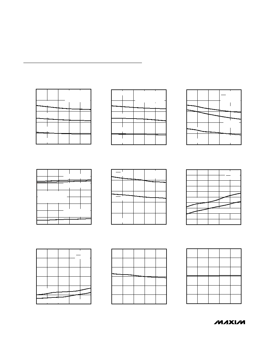
Typical Operating Characteristics
(V
CC1
= +5V, C
L
= 50pF (Figure 1), unless otherwise noted.)
I
CC1
SUPPLY CURRENT
vs. TEMPERATURE
MAX3535E toc01
TEMPERATURE (
∞C)
I
CC1
(mA)
60
35
10
-15
20
40
60
80
100
0
-40
85
FIGURE 1
R
L
= 27
R
L
= 60
R
L
= OPEN
HALO
TGM-250NS
1:1:1 TRANSFORMER
I
CC1
SUPPLY CURRENT
vs. TEMPERATURE
MAX3535E toc02
TEMPERATURE (
∞C)
I
CC1
(mA)
60
35
10
-15
20
40
60
80
100
0
-40
85
FIGURE 1
V
CC1
= +3.3V
R
L
= 60
R
L
= OPEN
HALO
TGM-240NS
1:1.3:1.3 TRANSFORMER
R
L
= 27
I
CC2
SUPPLY CURRENT
vs. TEMPERATURE
MAX3535E toc03
TEMPERATURE (
∞C)
I
CC2
(mA)
60
35
10
-15
40
50
60
70
80
30
-40
85
FIGURE 1
V
CC2
= +6V
f
DATA
= 700kbps
SLO = LOW
R
L
= 27
V
CC2
= +3.9V
(MAX3535E)
V
CC2
= +3.13V
(MAX3535E)
V
CC2
SUPPLY VOLTAGE
vs. TEMPERATURE
MAX3535E toc04
TEMPERATURE (
∞C)
V
CC2
(V)
60
35
-15
10
3.5
4.0
4.5
5.0
6.0
5.5
6.5
7.0
3.0
-40
85
HALO
TGM-240NS
1:1.3:1.3 TRANSFORMER
FIGURE 1
R
L
= OPEN, V
CC1
= +5V
R
L
= 27
, V
CC1
= +5V
R
L
= 27
, V
CC1
= +3V
(MAX3535E)
SELF-OSCILLATION FREQUENCY
vs. TEMPERATURE
MAX3535E toc05
TEMPERATURE (
∞C)
f
SOS
(kHz)
60
35
10
-15
300
350
400
450
500
250
-40
85
FIGURE 5
SLO = HIGH
V
CC1
= V
CC2
R
L
= 27
SLO = LOW
DRIVER DIFFERENTIAL OUTPUT
TRANSITION TIME vs. TEMPERATURE
MAX3535E toc06
TEMPERATURE (
∞C)
t
TD
(ns)
60
35
10
-15
10
20
30
40
50
60
70
80
90
100
0
-40
85
R
L
= 27
SLO = V
CC2
FIGURES 2, 6
V
CC2
= +5V
V
CC2
= +3.13V (MAX3535E)
DRIVER DIFFERENTIAL OUTPUT
TRANSITION TIME vs. TEMPERATURE
MAX3535E toc07
TEMPERATURE (
∞C)
t
TD
(ns)
60
35
10
-15
300
400
500
600
700
800
200
-40
85
R
L
= 27
SLO = GND2
FIGURES 2, 6
V
CC2
= +5V
V
CC2
= +3.13V (MAX3535E)
SWITCHER FREQUENCY
vs. TEMPERATURE
MAX3535E toc08
TEMPERATURE (
∞C)
f
SW
(kHz)
60
35
10
-15
350
400
450
500
550
600
300
-40
85
SWITCHER FREQUENCY
vs. SUPPLY VOLTAGE
MAX3535E toc09
V
CC1
(V)
f
SW
(kHz)
5.0
4.5
4.0
3.5
350
400
450
500
550
600
300
3.0
5.5
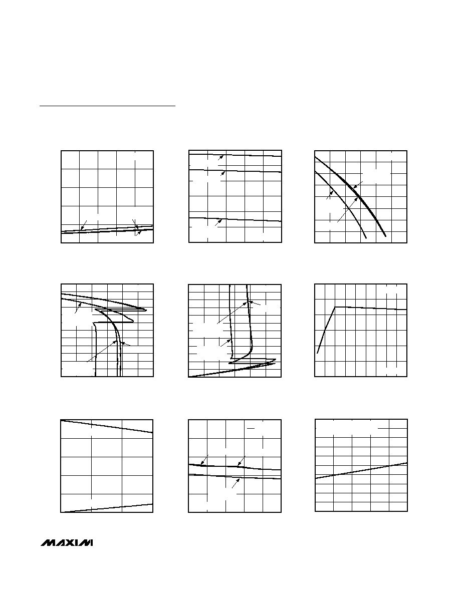
MAX3535E/MXL1535E
+3V to +5V, 2500V
RMS
Isolated RS-485/RS-422
Transceivers with ±15kV ESD Protection
______________________________________________________________________________________
11
RECEIVER-OUTPUT (RO1) LOW VOLTAGE
vs. TEMPERATURE
MAX3535E toc10
TEMPERATURE (
∞C)
V
RO1L
(V)
60
35
10
-15
0.2
0.4
0.6
0.8
1.0
0
-40
85
I
SINK
= 4mA
V
CC1
= +4.5V
V
CC1
= +3V
(MAX3535E)
V
CC1
= +5V
RECEIVER-OUTPUT (RO1) HIGH VOLTAGE
vs. TEMPERATURE
MAX3535E toc11
TEMPERATURE (
∞C)
V
RO1H
(V)
60
35
10
-15
2.5
3.0
3.5
4.0
4.5
5.0
2.0
-40
85
I
SOURCE
= 4mA
V
CC1
= +3V
(MAX3535E)
V
CC1
= +4.5V
V
CC1
= +5V
DRIVER DIFFERENTIAL OUTPUT VOLTAGE
vs. DIFFERENTIAL OUTPUT CURRENT
MAX3535E toc12
DRIVER DIFFERENTIAL OUTPUT CURRENT (mA)
V
OD
(V)
100
80
20
40
60
0.5
1.0
1.5
2.0
2.5
3.0
3.5
4.0
0
0
120
DE = HIGH
V
CC2
= +3.9V
(MAX3535E)
V
CC2
= +3.13V
(MAX3535E)
V
CC2
= +7.5V
DRIVER-OUTPUT HIGH VOLTAGE
vs. DRIVER SOURCE CURRENT
MAX3535E toc13
DRIVER SOURCE CURRENT (mA)
V
DOH
(V)
100
80
60
40
20
-6
-5
-4
-3
-2
-1
0
1
2
3
4
5
-7
0
120
DE = HIGH
V
CC2
= +3.13V
(MAX3535E)
V
CC2
= +3.9V
(MAX3535E)
V
CC2
= +7.5V
DRIVER-OUTPUT LOW VOLTAGE
vs. DRIVER SINK CURRENT
MAX3535E toc14
DRIVER SINK CURRENT (mA)
V
DOL
(V)
100
80
60
40
20
1
2
3
4
5
6
7
8
9
10
11
12
0
0
120
DE = HIGH
V
CC2
= +3.13V
(MAX3535E)
V
CC2
= +3.9V
(MAX3535E)
V
CC2
= +7.5V
DRIVER DIFFERENTIAL OUTPUT VOLTAGE
vs. V
CC2
SUPPLY VOLTAGE
MAX3535E toc15
V
CC2
(V)
V
OD
(V)
7.0
6.5
6.0
5.5
5.0
4.5
4.0
3.5
1.8
2.0
2.2
2.4
2.6
2.8
1.6
3.0
7.5
R
L
= 27
FIGURE 1
RECEIVER OUTPUT (RO1) VOLTAGE
vs. LOAD CURRENT
MAX3535E toc16
LOAD CURRENT (mA)
OUTPUT VOLTAGE (V)
10
5
1
2
3
4
5
0
0
15
OUTPUT HIGH, SOURCING
OUTPUT LOW, SINKING
DRIVER DIFFERENTIAL OUTPUT VOLTAGE
vs. TEMPERATURE
MAX3535E toc17
TEMPERATURE (
∞C)
V
OD
(V)
60
35
10
-15
1
2
3
4
5
0
-40
85
FIGURE 1
V
CC2
= +6V
R
L
= 27
SLO = GND2
V
CC2
= +3.13V
(MAX3535E)
V
CC2
= +7.5V
I
CC1
SUPPLY CURRENT
vs. V
CC1
SUPPLY VOLTAGE
MAX3535E toc18
V
CC1
SUPPLY VOLTAGE (V)
I
CC1
(mA)
5.0
4.5
4.0
3.5
1
2
3
4
5
6
7
8
9
10
0
3.0
5.5
R
L
= OPEN
TRANSFORMER IS NOT DRIVEN
Typical Operating Characteristics (continued)
(V
CC1
= +5V, C
L
= 50pF (Figure 1), unless otherwise noted.)
MAX3535E/MXL1535E
+3V to +5V, 2500V
RMS
Isolated RS-485/RS-422
Transceivers with ±15kV ESD Protection
12
______________________________________________________________________________________
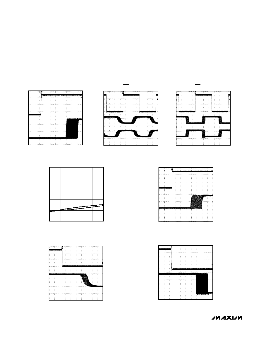
Typical Operating Characteristics (continued)
(V
CC1
= +5V, C
L
= 50pF (Figure 1), unless otherwise noted.)
RECEIVER (RO1) PROPAGATION DELAY
(t
PLH1
)
MAX3535E toc19
RO
1V/div
A-B
1V/div
100ns/div
DRIVER PROPAGATION DELAY
(SLO = LOW)
MAX3535E toc20
Y
2V/div
DI
2V/div
400ns/div
Z
2V/div
DRIVER PROPAGATION DELAY
(SLO = HIGH)
MAX3535E toc21
Y
2V/div
DI
2V/div
400ns/div
Z
2V/div
JITTER vs. TEMPERATURE
MAX3535E toc22
TEMPERATURE (
∞C)
t
J
(ns)
60
35
10
-15
220
240
260
280
300
200
-40
85
V
CC1
= 5.5V
V
CC1
= 3.13V
DRIVER ENABLE
TIME PLUS JITTER
MAX3535E toc23
Y
2V/div
DE
2V/div
200ns/div
DRIVER DISABLE
TIME PLUS JITTER
MAX3535E toc24
Y
2V/div
DE
2V/div
200ns/div
RECEIVER (RO1) PROPAGATION DELAY
(t
PHL1
)
MAX3535E toc25
RO
1V/div
A-B
1V/div
100ns/div
MAX3535E/MXL1535E
+3V to +5V, 2500V
RMS
Isolated RS-485/RS-422
Transceivers with ±15kV ESD Protection
______________________________________________________________________________________
13
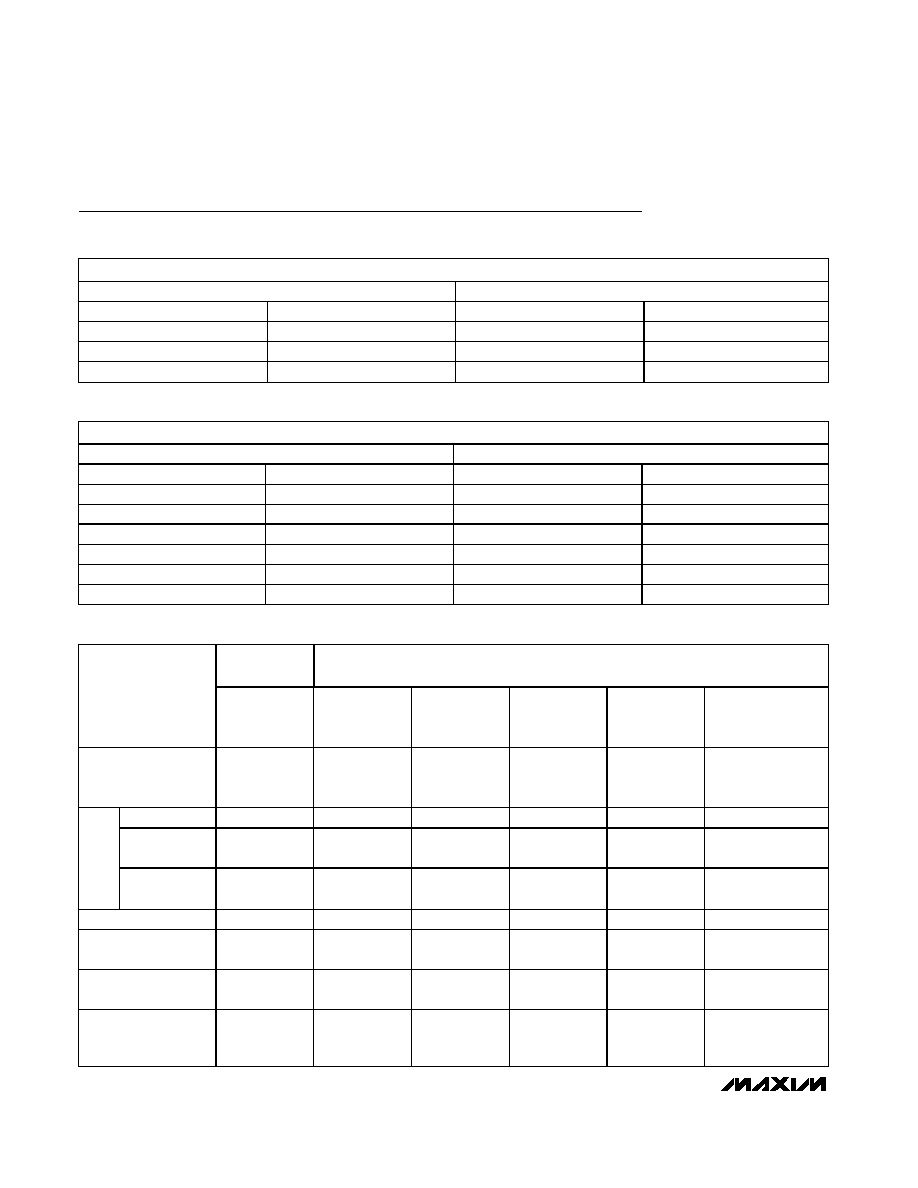
Pin Description
PIN
NAME
ISOLATION SIDE
FUNCTION
1
V
CC1
Logic
Logic-Side/Transformer-Driver Power Input. Bypass V
CC1
to GND1 with 10µF and 0.1µF
capacitors.
2
ST1
Logic
Transformer-Driver Phase 1 Power Output. Connect ST1 to isolation-transformer
primary to send power to isolation side of barrier.
3
ST2
Logic
Transformer-Driver Phase 2 Power Output. Connect ST2 to isolation-transformer
primary to send power to isolation side of barrier.
4
GND1
Logic
Logic-Side Ground. For isolated operation do not connect to GND2.
5≠10,
19≠24
--
--
Removed from Package
11
GND2
Isolated
Isolation-Side Ground. For isolated operation do not connect to GND1.
12
Z
Isolated
RS-485/RS-422 Inverting Driver Output. Output floats when DE is low or in a barrier fault
event. (See the Detailed Description section for more information.)
13
Y
Isolated
RS-485/RS-422 Noninverting Driver Output. Output floats when DE is low or in a barrier
fault event. (See the Detailed Description section for more information.)
14
V
CC2
Isolated
Isolated-Side Power Input. Connect V
CC2
to the rectified output of transformer
secondary. Bypass V
CC2
to GND2 with 10µF and 0.1µF capacitors.
15
B
Isolated
RS-485/RS-422 Differential-Receiver Inverting Input
16
A
Isolated
RS-485/RS-422 Differential-Receiver Noninverting Input
17
RO2
Isolated
Isol ated - S i d e Recei ver O utp ut. RO2 i s al w ays enab l ed . RO 2 g oes hi g h i f A - B > - 10m V .
RO2 g oes l ow i f A - B < - 200m V . Fai l - safe ci r cui tr y causes RO 2 to g o hi g h w hen A and B
fl oat or ar e shor ted .
18
SLO
Isolated
Driver Slew-Rate Control Logic Input. Connect SLO to GND2 for data rates up to
400kbps. Connect SLO to V
CC2
or leave floating for high data rates.
25
DI
Logic
Driver Input. Pull DI low (high) to force driver output Y low (high) and driver output Z
high (low).
26
DE
Logic
Driver-Enable Input. The driver outputs are enabled and follow the driver input (DI)
when DE is high. When DE is floated, the driver is disabled. DE does not affect whether
the receiver is on or off.
27
RE
Logic
Receiver-Output Enable and Fault Current Output. The receiver output (RO1) is
enabled and follows the differential-receiver inputs, A and B, when RE is low, otherwise
RO1 floats. RE does not affect RO2 and does not disable the driver. The asserted fault
output is a pullup current, otherwise RE shows a pulldown current.
28
RO1
Logic
Receiver Output. RO1 is enabled when RE is low. RO1 goes high if A - B > -10mV. RO1
goes low if A - B < -200mV. Fail-safe circuitry causes RO1 to go high when A and B
float or are shorted.
MAX3535E/MXL1535E
+3V to +5V, 2500V
RMS
Isolated RS-485/RS-422
Transceivers with ±15kV ESD Protection
14
______________________________________________________________________________________
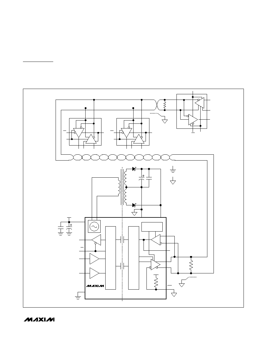
Test Circuits
R
L
R
L
V
OD
V
OC
Y
Z
Figure 1. Driver DC Test Load
DI
DE
HIGH
C
L
C
L
Y
Z
GND
GND2
R
L
R
L
Figure 2. Driver Timing Test Circuit
TGM-240
1/2
BAT54C
TRANSFORMER
DRIVER
BARRIER
TRANSCEIVER
ISOLATION BARRIER
BARRIER
TRANSCEIVER
1/2
BAT54C
VOLTAGE
REGULATOR
GND2
+3.0V TO +5.5V
DRIVER
RECEIVER
A
B
Y
Z
C
L
SLO
RO2
ST1
RO1
RE
DE
DI
GND1
ST2
V
CC2
V
CC1
V
CC2
0.1
µF
0.1
µF
CONTROL GROUND
RS485 GROUND
10
µF
10
µF
MAX3535E
C
L
2R
L
Figure 5. Self-Oscillating Configuration
500
V
CC2
C
L
Y/Z
GND2
500
Figure 3. Driver Timing Test Load
1k
V
CC1
/V
CC2
C
L
RO1/RO2
GND1/GND2
1k
Figure 4. Receiver Timing Test Load
MAX3535E/MXL1535E
+3V to +5V, 2500V
RMS
Isolated RS-485/RS-422
Transceivers with ±15kV ESD Protection
______________________________________________________________________________________
15
Switching Waveforms
DI
Z
Y
V
DOH
V
DOH
t
DD
t
DD
t
TD
t
TD
t
J
V
OD
= V
Y
- V
Z
t
R
< 10ns, t
F
< 10ns
1/2 V
DOH
0V
-V
DOH
20%
80%
1.5V
1.5V
80%
20%
Figure 6. Driver Propagation Delay
t
PLZ
V
DOL
+ 0.5V
V
DOH
- 0.5V
V
DOH
/2
V
DOH
/2
t
R
< 10ns, t
F
< 10ns
1.5V
1.5V
DE
V
DOH
Y, Z
V
DOL
V
DOH
0V
Y, Z
t
PZL
2 x t
J
t
PZH
t
J
t
PHZ
OUTPUT NORMALLY HIGH
OUTPUT NORMALLY LOW
Figure 7. Driver Enable and Disable Times
t
R
< 10ns, t
F
< 10ns
t
PLH1
V
RO1H
/2
80%
80%
20%
20%
V
RO1H
/2
OUTPUT
INPUT
0V
0V
V
A
- V
B
V
RO1H
V
RO1L
RO1
RO2
t
PLH1
t
PHL1
t
PLH2
t
PLH2
t
J
t
R
t
F
t
J
Figure 8. Receiver Propagation Delays
t
R
< 10ns, t
F
< 10ns
1.5V
1.5V
RE
V
RO1H
RO1
V
RO1L
V
RO1L
+ 0.5V
V
RO1H
- 0.5V
V
RO1H
RO1
0V
OUTPUT NORMALLY LOW
OUTPUT NORMALLY HIGH
t
HZ
t
LZ
t
ZL
t
ZH
Figure 9. Receiver Enable and Disable Times

MAX3535E/MXL1535E
+3V to +5V, 2500V
RMS
Isolated RS-485/RS-422
Transceivers with ±15kV ESD Protection
16
______________________________________________________________________________________
Detailed Description
The MAX3535E/MXL1535E isolated RS-485/RS-422 full-
duplex transceivers provide 2500V
RMS
of galvanic isola-
tion between the RS-485/RS-422 isolation side and the
processor or logic side. These devices allow fast,
1000kbps communication across an isolation barrier even
when the common-mode voltages (i.e., the ground poten-
tials) on either side of the barrier are subject to large dif-
ferences. The isolation barrier consists of two parts. The
first part is a capacitive isolation barrier (integrated high-
voltage capacitors) that allows data transmission
between the logic side and the RS-485/RS-422 isolation
side. Data is sampled and encoded before it is transmit-
ted across the isolation barrier introducing sampling jitter
and further delay into the communication system.
The second part of the isolation barrier consists of an
external transformer with the required primary-to-sec-
ondary isolation, allowing the transmission of operating
power from the logic side across the isolation barrier to
the isolation side. Connect the primary of the external
transformer to the MAX3535E/MXL1535E's 420kHz
transformer driver outputs ST1 and ST2. Since the
MXL1535E and the MAX3535E operate with different
supply-voltage requirements at their respective isolated
and logic sides, different isolation transformers must be
used with each device (see the Transformer Selection
section). The only external components needed to
complete the system are the isolation transformer, two
diodes, and two low-voltage, 10µF decoupling capaci-
tors (see the Typical Application Circuit).
The MAX3535E/MXL1535E include one differential dri-
ver, one receiver, and internal circuitry to send the RS-
485 signals and logic signals across the isolation barrier
(including the isolation capacitors). The MAX3535E/
MXL1535E receivers are 1/8 unit load, allowing up to 256
devices on a single bus.
The MAX3535E/MXL1535E feature fail-safe circuitry
ensuring the receiver output maintains a logic-high
state when the receiver inputs are open or shorted, or
when connected to a terminated transmission line with
all drivers disabled (see the Fail-Safe section).
The MAX3535E/MXL1535E feature driver slew-rate
select that minimizes electromagnetic interference
(EMI) and reduces reflections caused by improperly
terminated cables at data rates below 400kbps. The
driver outputs are short-circuit protected for sourcing or
sinking current and have overvoltage protection. Other
features include hot-swap capability, which holds the
driver off if the driver logic signals are floated after
power is applied. The MAX3535E/MXL1535E have
error-detection circuitry that alerts the processor when
there is a fault and disables the driver until the fault is
removed.
Fail Safe
The MAX3535E/MXL1535E guarantee a logic-high
receiver output when the receiver inputs are shorted or
open, or when connected to a terminated transmission
line with all drivers disabled. The receiver threshold is
fixed between -10mV and -200mV. If the differential
receiver input voltage (A - B) is greater than or equal to
-10mV, RO1 is logic-high (Table 2). In the case of a ter-
minated bus with all transmitters disabled, the receiv-
er's differential input voltage is pulled to zero by the
termination. Due to the receiver thresholds of the
MAX3535E/MXL1535E, this results in a logic-high at
RO1 with a 10mV minimum noise margin.
Driver Output Protection
Two mechanisms prevent excessive output current and
power dissipation caused by faults or by bus con-
tention. The first, a foldback current limit on the output
stage, provides immediate protection against short cir-
cuits over the entire common-mode voltage range. The
second, a thermal-shutdown circuit, forces the driver
outputs into a high-impedance state if the die tempera-
ture exceeds +150∞C.
Monitoring Faults on
RE
RE functions as both an input and an output. As an
input, RE controls the receiver output enable (RO1). As
an output, RE is used to indicate when there are faults
associated with the operation of the part. This dual
functionality is made possible by using an output driver
stage that can easily be overdriven by most logic
gates. When an external gate is not actively driving RE,
it is driven either high using a 100µA internal pullup
current (fault present), or low using a 60µA internal pull-
down current (no fault). When using RE to control the
receiver-enable output function, be sure to drive it
using a gate that has enough sink and source capabili-
ty to overcome the internal drive.
MAX3535E/MXL1535E
+3V to +5V, 2500V
RMS
Isolated RS-485/RS-422
Transceivers with ±15kV ESD Protection
______________________________________________________________________________________
17
When not actively driving RE, it functions as the fault
indicator (Table 3). A low on RE indicates the part is
functioning properly, while a high indicates a fault is
present. The four causes of a fault indication are:
1) The voltage on V
CC1
is below its undervoltage-lock-
out threshold (2.69V nominal)
2) The voltage on V
CC2
is below its undervoltage-lock-
out threshold (2.80V nominal)
3) There is a problem that prevents the MAX3535E/
MXL1535E from communicating across its isolation
barrier
4) The die temperature exceeds +150
∞C nominally,
causing the part to go into thermal shutdown
When a fault occurs, RO1 is switched to a logic-high
state if RE is low (Table 3). Open-circuit or short-circuit
conditions on the receiver inputs do not generate fault
conditions; however, any such condition also puts RO1
in a logic-high state (see the Fail Safe section).
Read RE for fault conditions by using a bidirectional
microcontroller I/O line or a tri-stated buffer as shown in
Figure 10. When using a tri-stated buffer, enable the
driver whenever the voltage on RE needs to be forced
to a logic-high or logic-low. To read RE for a fault con-
dition, disable the driver.
Slew-Rate Control Logic
The SLO input selects between a fast and a slow slew
rate for the driver outputs. Connecting SLO to GND2
selects the slow slew-rate option that minimizes EMI
and reduces reflections caused by improperly terminat-
ed cables at data rates up to 400kbps. This occurs
because lowering the slew rate decreases the rise and
fall times for the signal at the driver outputs, drastically
reducing the high-frequency components and harmon-
ics at the output. Floating SLO or connecting it to V
CC2
selects the fast slew rate, which allows high-speed
operation.
RO1
RE
DE
DI
GND1
RE
OE
FAULT
V
CC1
V
CC1
TRI-STATED BUFFER/
BIDIRECTIONAL MICROCONTROLLER I/O
FAULT
DRIVER OUTPUT BECOMES HIGH IMPEDANCE
FAULT DETECTED
OE
R
MAX3535E
MXL1535E
D
Figure 10. Reading a Fault Condition
MAX3535E/MXL1535E
+3V to +5V, 2500V
RMS
Isolated RS-485/RS-422
Transceivers with ±15kV ESD Protection
18
______________________________________________________________________________________
Functional Tables
Table 1. Transmitting Logic
TRANSMITTING LOGIC
INPUTS
OUTPUTS
DE
DI
Y
Z
1
1
1
0
1
0
0
1
0
X
High impedance
High impedance
Table 2. Receiving Logic
RECEIVING LOGIC
INPUTS
OUTPUTS
RE
V
A
- V
B
RO1
RO2
0
>-10mV
1
1
0
<-200mV
0
0
0
Inputs open/shorted
1
1
1
>-10mV
High impedance
1
1
<-200mV
High impedance
0
1
Inputs open/shorted
High impedance
1
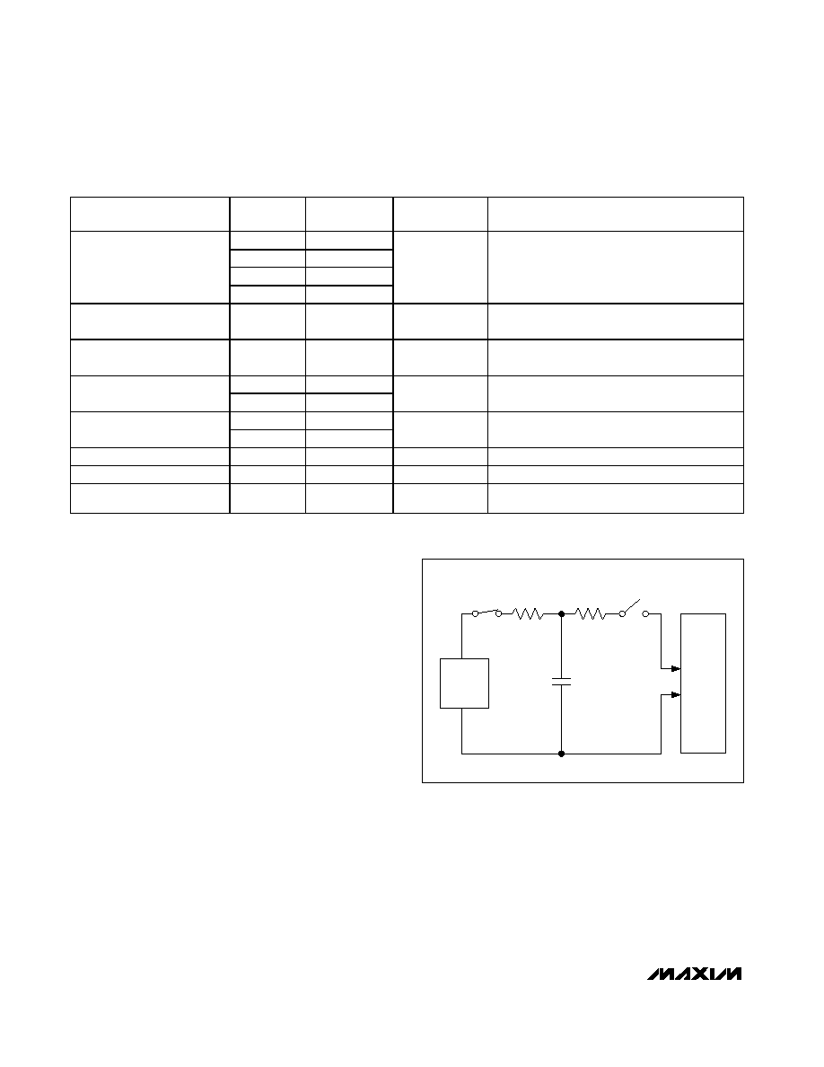
Table 3. Fault Mode
NORMAL
MODE
FAULT MODES
FUNCTION
V
CC1
> V
UVH1
V
CC2
> V
UVH2
V
CC1
< V
UVL1
V
CC2
> V
UVH2
V
CC1
> V
UVH1
V
CC2
< V
UVL2
V
CC1
< V
UVL1
V
CC2
< V
UVL2
THERMAL
SHUTDOWN
INTERNAL
COMMUNICATION
FAULT
Transformer
driver
(ST1, ST2)
On
On
On
On
Off
On
RE = 0
Active
High
High
High
High
High
RE = V
CC1
High
impedance
High
impedance
High
impedance
High
impedance
High
impedance
High impedance
RO1
RE = floating
Active
High
impedance
High
impedance
High
impedance
High
impedance
High impedance
RO2
Active
Active
Active
Active
Active
Active
Driver outputs (Y, Z)
Active
High
impedance
High
impedance
High
impedance
High
impedance
High impedance
Internal barrier
communication
Active
Disabled
Disabled
Disabled
Disabled
Communication
attempted
Fault indicator on RE
Low
(60µA pull-
down)
High
(100µA pullup)
High
(100µA pullup)
High
(100µA pullup)
High
(100µA pullup)
High
(100µA pullup)
MAX3535E/MXL1535E
+3V to +5V, 2500V
RMS
Isolated RS-485/RS-422
Transceivers with ±15kV ESD Protection
______________________________________________________________________________________
19
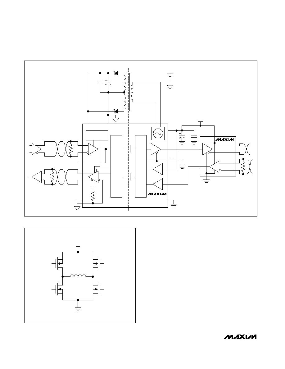
Applications Information
Typical Applications
The MAX3535E/MXL1535E transceivers facilitate bi-
directional data communications on multipoint bus
transmission lines. Figure 11 shows a typical RS-485
multidrop-network applications circuit. Figure 12 shows
the MAX3535E/MXL1535E functioning as line repeaters
with cable lengths longer than 4000ft. To minimize
reflections, terminate the line at both ends in its charac-
teristic impedance. Keep stub lengths off the main line
as short as possible.
DI
DE
RO
TGM-240
1/2
BAT54C
TRANSFORMER
DRIVER
BARRIER
TRANSCEIVER
ISOLATION BARRIER
BARRIER
TRANSCEIVER
1/2
BAT54C
VOLTAGE
REGULATOR
B
A
R
D
RE
RO
DE
DI
R
120
D
A
B
RE
RE
DI
DE
RO
B
A
R
D
GND2
+3.3V
DRIVER
RECEIVER
A
B
Y
Z
SLO
RO2
ST1
RO1
RE
DE
DI
GND1
ST2
V
CC2
V
CC1
V
CC2
120
0.1
µF
0.1
µF
CONTROL GROUND
RS-485 GROUND
10
µF
10
µF
MAX3535E
R
D
Figure 11. Typical Half-Duplex Multidrop RS-485 Network
Transformer Selection
The MXL1535E is a pin-for-pin compatible upgrade of
the LTC1535, making any transformer designed for that
device suitable for the MXL1535E (see Table 4). These
transformers all have a turns ratio of about 1:1.3CT.
The MAX3535E can operate with any of the transformers
listed in Table 4, in addition to smaller, thinner transform-
ers designed for the MAX845 and MAX253. The 420kHz
transformer driver operates with single primary and cen-
ter-tapped secondary transformers. When selecting a
transformer, do not exceed its ET product, the product of
the maximum primary voltage and half the highest period
of oscillation (lowest oscillating frequency). This ensures
that the transformer does not enter saturation. Calculate
the minimum ET product for the transformer primary as:
ET = V
MAX
/ (2 x f
MIN
)
where, V
MAX
is the worst-case maximum supply voltage,
and f
MIN
is the minimum frequency at that supply voltage.
Using +5.5V and 290kHz gives a required minimum ET
MAX3535E/MXL1535E
+3V to +5V, 2500V
RMS
Isolated RS-485/RS-422
Transceivers with ±15kV ESD Protection
20
______________________________________________________________________________________
TGM-250
1/2
BAT54C
TRANSFORMER
DRIVER
BARRIER
TRANSCEIVER
ISOLATION BARRIER
BARRIER
TRANSCEIVER
1/2
BAT54C
VOLTAGE
REGULATOR
GND2
+5V
DRIVER
RECEIVER
A
B
Y
Z
Y
Z
SLO
RO2
ST1
RO1
RO
RE
DE
DI
DI
GND1
ST2
V
CC2
V
CC1
V
CC2
0.1
µF
0.1
µF
CONTROL GROUND
RS-422 GROUND
10
µF
10
µF
MAX3535E
MXL1535E
MAX488
R
D
A
B
120
120
R
D
D
R
Figure 12. Using the MAX3535E/MXL1535E as an RS-422 Line Repeater
V
CC1
R
OH
R
OH
R
OL
R
OL
TRANSFORMER DRIVER OUTPUT STAGE
TRANSFORMER
PRIMARY
GND1
ST1
ST2
Figure 13. Transformer Driver Output Stage
MAX3535E/MXL1535E
+3V to +5V, 2500V
RMS
Isolated RS-485/RS-422
Transceivers with ±15kV ESD Protection
______________________________________________________________________________________
21
product of 9.5V-µs. The commercially available trans-
formers for the MAX845 listed in Table 5 meet that
requirement. In most cases, use half of the center-tapped
primary winding with the MAX3535E and leave the other
end of the primary floating. Most of the transformers in
Table 5 are 1:1:1 or 1:1:1:1 turns ratio.
For +3.3V operation (+3.6V maximum) the required pri-
mary ET product is 6.2V-µs. All of the previously men-
tioned transformers meet this requirement. Table 6 lists
some other transformers with step-up turns ratios
specifically tailored for +3.3V operation. Most of the
transformers in Table 6 are 1:1:1.3:1.3.
By using a HALO TGM-010 or Midcom 95061 trans-
former, it becomes possible to build a complete isolated
RS-485/RS-422 transceiver with a maximum thickness
less than 0.1in. To minimize power consumption, select
the turns ratio of the transformer to produce the minimum
DC voltage required at V
CC2
(+3.13V) under worst-case,
high-temperature, low-V
CC1
, and full-load conditions. For
light loads on the isolated side, ensure that the voltage at
V
CC2
does not exceed +7.5V. For example, the CTX01-
14659 transformer results in 85mA (typ) V
CC1
supply cur-
rent with full load on the RS-485 driver. Using a TGM250
1:1:1 transformer lowers the V
CC1
supply current to 65mA
(typ), while maintaining good margin on the V
CC2
supply.
A slight step-down transformer can result in extra power
savings in some situations. A custom wound sample
transformer with 23 primary turns and 20:20 secondary
turns on a Ferronics 11-050B core operates well with a
V
CC1
supply current of 51mA (typ).
Table 4. Transformers for the MXL1535E/MAX3535E
MANUFACTURER
PART NUMBER
ISOLATION VOLTAGE (1s)
PHONE NUMBER
Cooper Electronic Technologies, Inc.
CTX01-14659
500V
561-241-7876
Cooper Electronic Technologies, Inc.
CTX01-14608
3750V
RMS
561-241-7876
EPCOS AG (Germany)
(USA)
B78304-A1477-A3
500V
0 89-626-2-80-00
800-888-7724
Midcom, Inc.
31160R
1250V
605-886-4385
Pulse FEE (France)
P1597
500V
33-3-85-35-04-04
Sumida Corporation (Japan)
S-167-5779
100V
03-3667-3320
Transpower Technologies, Inc.
TTI7780-SM
500V
775-852-0145
Table 5. Transformers for MAX3535E at +5V
MANUFACTURER
PART
NUMBER
ISOLATION
VOLTAGE (1s)
PHONE
NUMBER
WEBSITE
TGM-010
500V
RMS
TGM-250
2000V
RMS
TGM-350
3000V
RMS
HALO Electronics, Inc.
TGM-450
4500V
RMS
650-903-3800
www.haloelectronics.com/6pin.html
BH Electronics, Inc.
500-1749
3750V
RMS
952-894-9590
www.bhelectronics.com/PDFs/DC-
DCConverterTransformers.pdf
Coilcraft, Inc.
U6982-C
1500V
RMS
800-322-2645
44-1236-730595
www.coilcraft.com/minitrans.cfm
7825355
1500V
Newport/C&D Technologies
7625335
4000V
520-295-4300
www.dc-dc.com/products/productline.asp?ED=9
Midcom, Inc.
95061
1250V
605-886-4385
www.midcom-inc.com
PCA Electronics, Inc.
EPC3115S-5
700V DC
818-894-5791
www.pca.com/Datasheets/EPC3117S-X.pdf
Rhom b us Ind ustr i es, Inc.
T-1110
1800V
RMS
714-898-0960
www.rhombus-ind.com/pt-cat/maxim.pdf
Premier Magnetics, Inc.
PM-SM15
1500V
RMS
949-452-0511
www.premiermag.com/pdf/pmsm15.pdf
±15kV ESD Protection
As with all Maxim devices, ESD-protection structures
are incorporated on all pins to protect against electro-
static discharges encountered during handling and
assembly. The driver outputs and receiver inputs have
extra protection against static electricity. Maxim's engi-
neers have developed state-of-the-art structures to pro-
tect these pins against ESD of ±15kV without damage.
The ESD structures withstand high ESD in all states.
After an ESD event, the MAX3535E/MXL1535E keep
working without latchup. ESD protection can be tested
in various ways. The transmitter outputs and receiver
inputs of this product family are characterized for pro-
tection to ±15kV using the Human Body Model.
ESD Test Conditions
The ±15kV ESD test specifications apply only to the A,
B, Y, and Z I/O pins. The test surge is referenced to
GND2. All remaining pins are ±2kV ESD protected.
Human Body Model
Figure 14 shows the Human Body Model, and Figure
15 shows the current waveform it generates when dis-
charged into low impedance. This model consists of a
100pF capacitor charged to the ESD voltage of interest,
which is then discharged into the test device through a
1.5k
resistor.
MAX3535E/MXL1535E
+3V to +5V, 2500V
RMS
Isolated RS-485/RS-422
Transceivers with ±15kV ESD Protection
22
______________________________________________________________________________________
Table 6. Transformers for MAX3535E at +3.3V
MANUFACTURER
PART
NUMBER
ISOLATION
VOLTAGE (1s)
PHONE
NUMBER
WEBSITE
TGM-040
500V
RMS
TGM-240
2000V
RMS
TGM-340
3000V
RMS
HALO Electronics, Inc.
TGM-340
4500V
RMS
650-903-3800
www.haloelectronics.com/6pin.html
BH Electronics, Inc.
500-2582
2000V
RMS
952-894-9590
www.bhelectronics.com/PDFs/DC-
DCConverterTransformers.pdf
Coilcraft, Inc.
Q4470-C
1500V
RMS
800-322-2645
44-1236-730595
www.coilcraft.com/minitrans.cfm
78253335
1500V
Newport/C&D Technologies
76253335
4000V
520-295-4300
www.dc-dc.com/products/productline.asp?ED=9
95062
1250V
Midcom, Inc.
95063
1250V
605-886-4385
www.midcom-inc.com
PCA Electronics, Inc.
EPC3115S-2
700V DC
818-894-5791
www.pca.com/Datasheets/EPC3117S-X.pdf
Rhom b us Ind ustr i es, Inc.
T-1107
1800V
RMS
714-898-0960
www.rhombus-ind.com/pt-cat/maxim.pdf
Premier Magnetics Inc.
PM-SM16
1500V
RMS
949-452-0511
www.premiermag.com/pdf/pmsm15.pdf
CHARGE-CURRENT-
LIMIT RESISTOR
DISCHARGE
RESISTANCE
STORAGE
CAPACITOR
Cs
100pF
R
C
1M
R
D
1500
HIGH-
VOLTAGE
DC
SOURCE
DEVICE
UNDER
TEST
Figure 14. Human Body ESD Test Model
MAX3535E/MXL1535E
+3V to +5V, 2500V
RMS
Isolated RS-485/RS-422
Transceivers with ±15kV ESD Protection
______________________________________________________________________________________
23
Machine Model
The Machine Model for ESD tests all pins using a
200pF storage capacitor and zero discharge resis-
tance. Its objective is to simulate the stress caused by
contact that occurs with handling and assembly during
manufacturing. All pins require this protection during
manufacturing, not just inputs and outputs. Therefore,
after PC board assembly, the Machine Model is less
relevant to I/O ports.
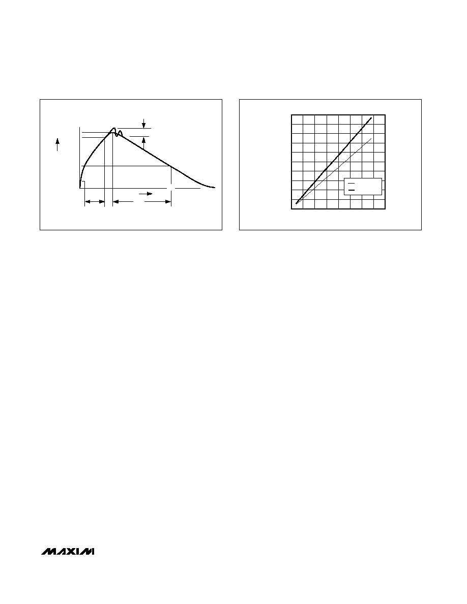
Skew
The self-oscillation circuit shown in Figure 5 is an excel-
lent way to get an approximate measure of the speed
of the MAX3535E/MXL1535E. An oscillation frequency
of 250kHz in this configuration implies a data rate of at
least 500kbps for the receiver and transmitter com-
bined. In practice, data can usually be sent and
received at a considerably higher data rate, normally
limited by the allowable jitter and data skew. If the sys-
tem can tolerate a 25% data skew, (the difference
between t
PLH1
and t
PHL1
), the 285ns maximum jitter
specification implies a data rate of 877kbps. Lower
data rates result in less distortion and jitter (Figure 16).
Higher rates are possible but with more distortion and
jitter. The data rate should always be limited below
1.75Mbps for both receiver and driver to avoid interfer-
ence with the internal barrier communication.
Layout Considerations
The MAX3535E/MXL1535E pin configurations enable
optimal PC board layout by minimizing interconnection
lengths and crossovers:
∑ For maximum isolation, the isolation barrier should not
be breached except by the MAX3535E/MXL1535E and
the transformer. Connections and components from
one side of the barrier should not be located near those
of the other side of barrier.
∑ A shield trace connected to the ground on each side of
the barrier can help intercept capacitive currents that
might otherwise couple into the DI and SOL inputs. In a
double-sided or multilayer board, these shield traces
should be present on all conductor layers.
∑ Try to maximize the width of the isolation barrier
wherever possible. A clear space of at least 0.25in
between GND1 and GND2 is recommended.
I
P
100%
90%
36.8%
t
RL
TIME
t
DL
CURRENT WAVEFORM
PEAK-TO-PEAK RINGING
(NOT DRAWN TO SCALE)
Ir
10%
0
0
AMPERES
Figure 15. Human Body Current Waveform
0
10
5
20
15
30
25
35
45
40
50
0
500 750
250
1000 1250 1500 1750 2000
DATA SKEW vs. DATA RATE
DATA RATE (kbps)
DATA SKEW (%)
TYP SKEW
MAX SKEW
Figure 16. Data Skew vs. Data Rate Graph
MAX3535E/MXL1535E
+3V to +5V, 2500V
RMS
Isolated RS-485/RS-422
Transceivers with ±15kV ESD Protection
24
______________________________________________________________________________________
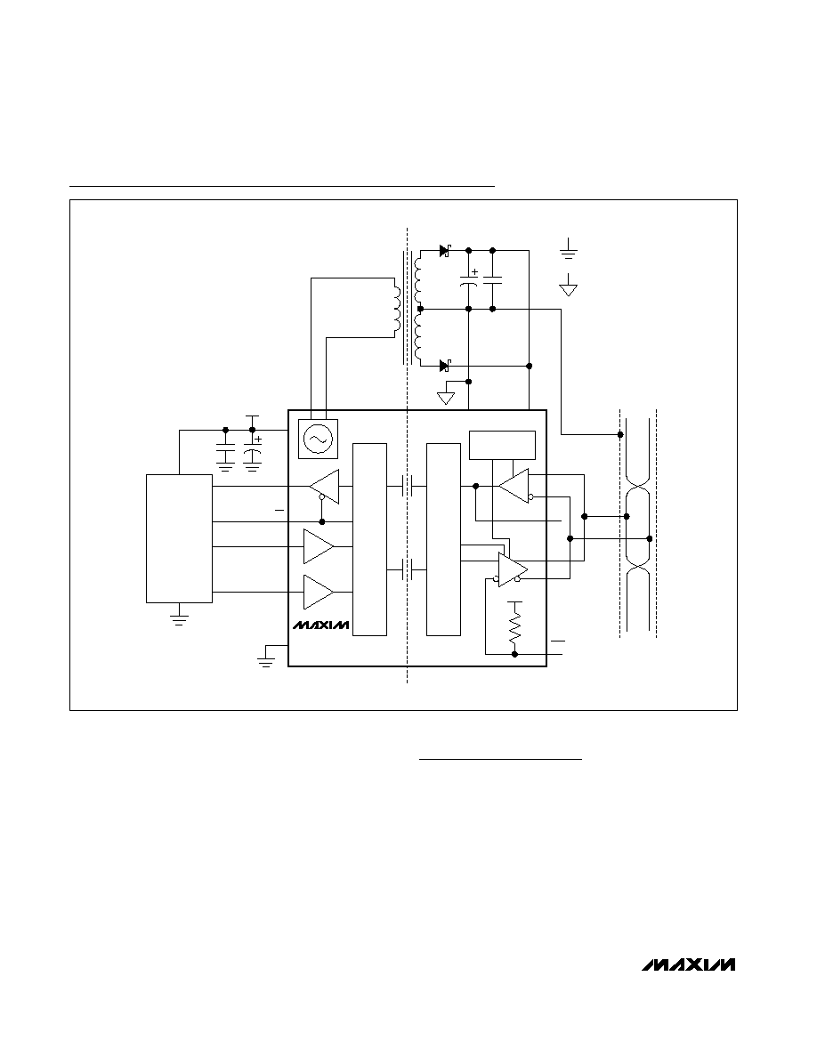
Chip Information
PROCESS: BiCMOS
TRANSISTOR COUNT: 7379
TGM-240
1/2
BAT54C
TRANSFORMER
DRIVER
BARRIER
TRANSCEIVER
ISOLATION BARRIER
BARRIER
TRANSCEIVER
1/2
BAT54C
VOLTAGE
REGULATOR
GND2
+3.3V
DRIVER
RECEIVER
A
B
Y
Z
SLO
RO2
ST1
RO1
µC
RE
DE
DI
GND1
ST2
V
CC2
V
CC1
V
CC2
0.1
µF
0.1
µF
CONTROL GROUND
RS-485 GROUND
10
µF
10
µF
MAX3535E
Typical Application Circuit
MAX3535E/MXL1535E
+3V to +5V, 2500V
RMS
Isolated RS-485/RS-422
Transceivers with ±15kV ESD Protection
Maxim cannot assume responsibility for use of any circuitry other than circuitry entirely embodied in a Maxim product. No circuit patent licenses are
implied. Maxim reserves the right to change the circuitry and specifications without notice at any time.
Maxim Integrated Products, 120 San Gabriel Drive, Sunnyvale, CA 94086 408-737-7600 ____________________ 25
© 2004 Maxim Integrated Products
Printed USA
is a registered trademark of Maxim Integrated Products.
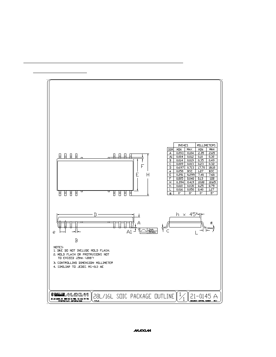
Package Information
(The package drawing(s) in this data sheet may not reflect the most current specifications. For the latest package outline information
go to www.maxim-ic.com/packages.)
28L 16L SOIC.EPS