2.25MHZ 400mA/600mA Dual Step Down Converters In Small 3x3mm2 QFN Pkg (Rev. A)
www.ti.com
FEATURES
DESCRIPTION
APPLICATIONS
0
10
20
30
40
50
60
70
80
90
100
0.01
0.1
1
10
100
1000
IOUTmA
E
f
f
i
c
i
e
n
c
y
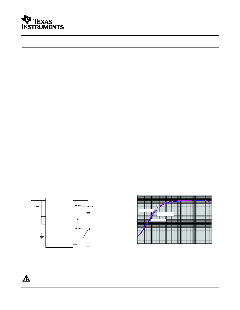
VIN = 3.6 V
MODE/DATA = 0
VOUT1= 1.575 V
VOUT2 = 1.8 V
V
: 1.575 V
400 mA
out1
SW1
FB 1
SW2
ADJ2
DEF_1
10 F
m
VIN 2.5 V 6 V
VIN
EN_1
EN_2
MODE/
DATA
TPS62401
GND
2.2 H
m
10 F
m
2.2 H
m
V
: 1.8 V
600 mA
out2
10 F
m
TPS62400
TPS62401
SLVS681A JUNE 2006 REVISED JULY 2006
2.25MHz 400mA/600mA Dual Step-Down Converter In Small 3x3mm QFN Package
·
High Efficiency--Up to 95%
The TPS6240x device series are synchronous dual
step-down DC-DC converters optimized for battery
·
V
IN
Range From 2.5 V to 6 V
powered portable applications. They provide two
·
2.25 MHz Fixed Frequency Operation
independent output voltage rails powered by 1-cell
·
Output Current 400 mA and 600 mA
Li-Ion or 3-cell NiMH/NiCD batteries. The devices are
·
Adjustable Output Voltage From 0.6V to V
IN
also suitable to operate from a standard 3.3V or 5V
voltage rail.
·
EasyScaleTM Optional One-Pin Serial Interface
for Dynamic Output Voltage Adjustment
With an input voltage range of 2.5V to 6V the
TPS62400 is ideal to power portable applications like
·
TPS62401 Fixed Output Voltage Option:
smart phones, PDAs and other portable equipment.
1.1V/1.575V 400mA
With the EasyScaleTM serial interface the output
1.8V 600mA
voltages
can
be
modified
during
operation.
It
·
Power Save Mode at Light Load Currents
therefore supports Dynamic Voltage Scaling for low
·
180
°
Out of Phase Operation
power DSP and processors.
·
Output Voltage Accuracy in PWM Mode
±
1%
The TPS62401 provides fixed output voltages of
·
Typical 32-
µ
A Quiescent Current for both
1.1V/1.575V and 1.8V.
Converters
The TPS6240x operates at 2.25MHz fixed switching
·
100% Duty Cycle for Lowest Dropout
frequency;
and,
enters
the
power
save
mode
operation at light load currents to maintain high
·
Available in a 10-Pin QFN (3
×
3mm)
efficiency over the entire load current range. For low
noise applications the devices can be forced into
fixed
frequency
PWM
mode
by
pulling
the
·
Cell Phones, Smart-phones
MODE/DATA pin high. In the shutdown mode, the
·
PDAs, Pocket PCs
current consumption is reduced to 1.2
µ
A, typical.
·
OMAPTM and Low Power DSP Supply
The devices allow the use of small inductors and
capacitors to achieve a small solution size.
·
Portable Media Players
·
Digital Radio
The TPS62400 is available in a 10-pin leadless
package (3
×
3mm QFN)
·
Digital Cameras
Please be aware that an important notice concerning availability, standard warranty, and use in critical applications of Texas
Instruments semiconductor products and disclaimers thereto appears at the end of this data sheet.
EasyScale, OMAP, PowerPad, PowerPAD are trademarks of Texas Instruments.
PRODUCTION DATA information is current as of publication date.
Copyright © 2006, Texas Instruments Incorporated
Products conform to specifications per the terms of the Texas
Instruments standard warranty. Production processing does not
necessarily include testing of all parameters.
www.ti.com
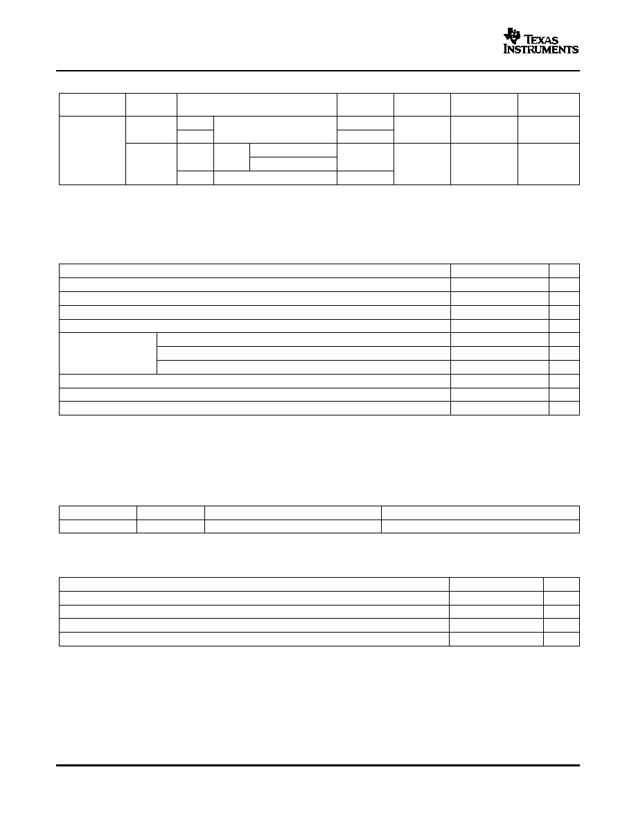
ABSOLUTE MAXIMUM RATINGS
DISSIPATION RATINGS
RECOMMENDED OPERATING CONDITIONS
TPS62400
TPS62401
SLVS681A JUNE 2006 REVISED JULY 2006
ORDERING INFORMATION
T
A
PART
DEFAULT OUTPUT
OUTPUT
QFN
(2)
ORDERING
PACKAGE
NUMBER
VOLTAGE
(1)
CURRENT
PACKAGE
MARKING
OUT1
400mA
TPS62400
Adjustable
DRC
TPS62400DRC
BQE
OUT2
600mA
40
°
C to 85
°
C
DEF_1 = High 1.1V
Fixed
OUT1
400mA
default
TPS62401
DEF_1 = Low 1.575V
DRC
TPS62401DRC
BRN
OUT2
Fixed default 1.8V
600mA
(1)
Contact TI for other fixed output voltage options.
(2)
The DRC (QFN 10 PIN) package is available in tape on reel. Add R suffix to order quantities of 3000 parts per reel.
over operating free-air temperature range (unless otherwise noted)
(1)
VALUE
UNIT
Input voltage range on V
IN
(2)
0.3 to 7
V
Voltage range on EN, MODE/DATA, DEF_1
0.3 to V
IN
+0.3,
7
V
Voltage on SW1, SW2
0.3 to 7
V
Voltage on ADJ2, FB1
0.3 to V
IN
+0.3,
7
V
HBM Human body model
2
kV
ESD
Charge device model CDM
1
kV
rating
(3)
Machine model
200
V
T
J
(max)
Maximum operating junction temperature
150
°
C
T
A
Operating ambient temperature range
40 to 85
°
C
T
stg
Storage temperature range
65 to 150
°
C
(1)
Stresses beyond those listed under absolute maximum ratings may cause permanent damage to the device. These are stress ratings
only, and functional operation of the device at these or any other conditions beyond those indicated under recommended operating
conditions is not implied. Exposure to absolutemaximumrated conditions for extended periods may affect device reliability.
(2)
All voltage values are with respect to network ground terminal.
(3)
The human body model is a 100pF capacitor discharged through a 1.5k
resistor into each pin. The machine model is a 200pF
capacitor discharged directly into each pin.
PACKAGE
R
JA
POWER RATING FOR T
A
25
°
C
DERATING FACTOR ABOVE T
A
= 25
°
C
DRC
49
°
C/W
2050mW
21mW/
°
C
over operating free-air temperature range (unless otherwise noted)
MIN
NOM
MAX
UNIT
VIN
Supply voltage
2.5
6
V
Output voltage range for adjustable voltage
0.6
VIN
V
T
A
Operating ambient temperature
-40
85
°
C
T
J
Operating junction temperature
-40
125
°
C
2
Submit Documentation Feedback
www.ti.com
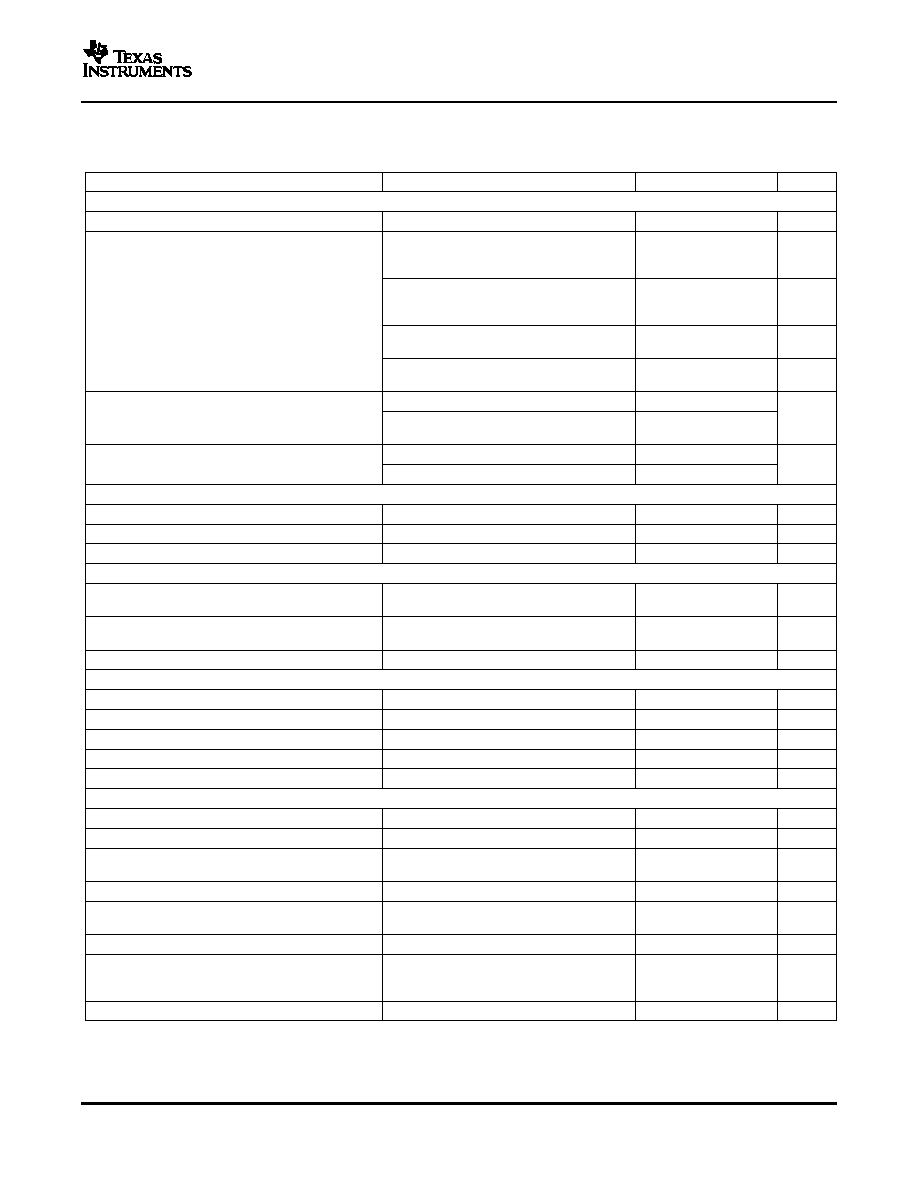
ELECTRICAL CHARACTERISTICS
TPS62400
TPS62401
SLVS681A JUNE 2006 REVISED JULY 2006
V
IN
= 3.6V, V
OUT
= 1.8V, EN = V
IN
, MODE = GND, L = 2.2
µ
H, C
OUT
= 20
µ
F, T
A
= 40
°
C to 85
°
C typical values are at T
A
=
25
°
C (unless otherwise noted)
PARAMETER
TEST CONDITIONS
MIN
TYP
MAX
UNIT
SUPPLY CURRENT
V
IN
Input voltage range
2.5
6.0
V
One converter, I
OUT
= 0mA. PFM mode
19
29
µ
A
enabled (Mode = 0) device not switching,
EN1 = 1 OR EN2 = 1
Two converter, I
OUT
= 0mA. PFM mode
32
48
µ
A
enabled (Mode = 0) device not switching,
I
Q
Operating quiescent current
EN1 = 1 AND EN2 = 1
I
OUT
= 0mA, MODE/DATA = GND, for one
23
µ
A
converter, V
OUT
1.575V
(1)
I
OUT
= 0mA, MODE/DATA = V
IN
, for one
3.6
mA
converter, V
OUT
1.575V
(1)
EN1, EN2 = GND, V
IN
= 3.6V
(2)
1.2
3
I
SD
Shutdown current
µ
A
EN1, EN2 = GND, V
IN
ramped from 0V to
0.1
1
3.6V
(3)
Falling
1.5
2.35
V
UVLO
Undervoltage lockout threshold
V
Rising
2.4
ENABLE EN1, EN2
V
IH
High-level input voltage, EN1, EN2
1.2
V
IN
V
V
IL
Low-level input voltage, EN1, EN2
0
0.4
V
I
IN
Input bias current, EN1, EN2
EN1, EN2 = GND or VIN
0.05
1.0
µ
A
DEF_1 INPUT
V
DEF_1H
DEF_1 high level input voltage
DEF_1 pin is a digital input at TPS62401
0.9
V
IN
V
fixed output voltage option
V
DEF_1L
DEF_1 low level input voltage
DEF_1 pin is a digital input at TPS62401
0
0.4
V
fixed output voltage option
I
IN
Input bias current DEF_1
DEF_1 GND or VIN
0.01
1.0
µ
A
MODE/DATA
V
IH
High-level input voltage, MODE/DATA
1.2
V
IN
V
V
IL
Low-level input voltage, MODE/DATA
0
0.4
V
I
IN
Input bias current, MODE/DATA
MODE/DATA = GND or VIN
0.01
1.0
µ
A
V
OH
Acknowledge output voltage high
Open drain, via external pullup resistor
V
IN
V
V
OL
Acknowledge output voltage low
Open drain, sink current 500
µ
A
0
0.4
V
INTERFACE TIMING
t
Start
Start time
2
µ
s
t
H_LB
High time low bit, logic 0 detection
Signal level on MODE/DATA pin is > 1.2V
2
200
µ
s
t
L_LB
Low time low bit, logic 0 detection
Signal level on MODE/DATA pin < 0.4V
2x
400
µ
s
t
H_LB
t
L_HB
Low time high bit, logic 1 detection
Signal level on MODE/DATA pin < 0.4V
2
200
µ
s
t
H_HB
High time high bit, logic 1 detection
Signal level on MODE/DATA pin is > 1.2V
2x
400
µ
s
t
L_HB
T
EOS
End of Stream
T
EOS
2
µ
s
t
ACKN
Duration of acknowledge condition
V
IN
2.5V to 6V
400
520
µ
s
(MODE/DATE line pulled low by the
device)
t
valACK
Acknowledge valid time
2
µ
s
(1)
Device is switching with no load on the output, L = 3.3
µ
H, value includes losses of the coil
(2)
These values are valid after the device has been already enabled one time (EN1 or EN2 = high) and supply voltage V
IN
has not
powered down.
(3)
These values are valid when the device is disabled (EN1 and EN2 low) and supply voltage V
IN
is powered up. The values remain valid
until the device has been enabled first time (EN1 or EN2 = high). After first enable, Note 3 becomes valid.
3
Submit Documentation Feedback
www.ti.com
TPS62400
TPS62401
SLVS681A JUNE 2006 REVISED JULY 2006
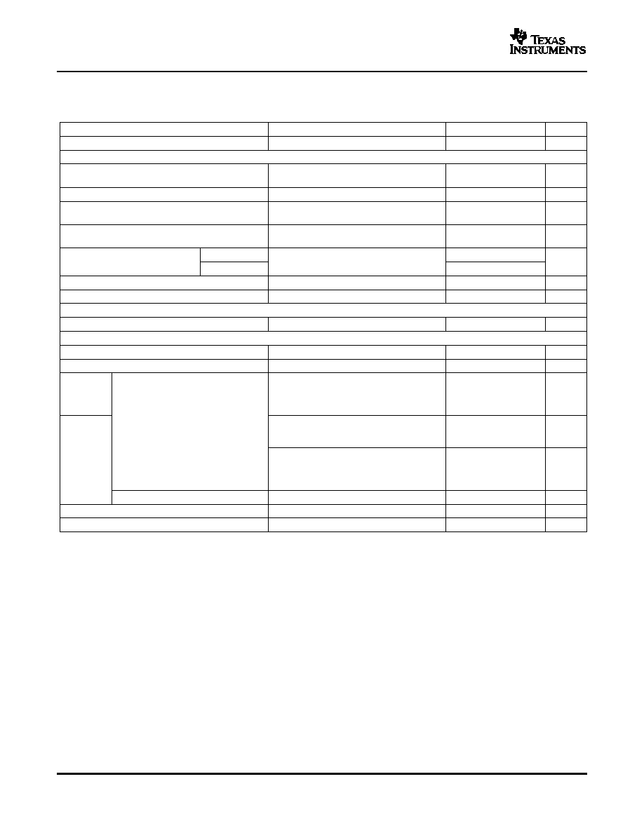
ELECTRICAL CHARACTERISTICS (continued)
V
IN
= 3.6V, V
OUT
= 1.8V, EN = V
IN
, MODE = GND, L = 2.2
µ
H, C
OUT
= 20
µ
F, T
A
= 40
°
C to 85
°
C typical values are at T
A
=
25
°
C (unless otherwise noted)
PARAMETER
TEST CONDITIONS
MIN
TYP
MAX
UNIT
t
timeout
Timeout for entering power save mode
MODE/DATA Pin changes from high to low
520
µ
s
POWER SWITCH
R
DS(ON)
P-Channel MOSFET on-resistance,
V
IN
= V
GS
= 3.6V
280
620
m
Converter 1,2
I
LK_PMOS
P-Channel leakage current
V
DS
= 6.0V
1
µ
A
R
DS(ON)
N-Channel MOSFET on-resistance
V
IN
= V
GS
= 3.6V
200
450
m
Converter 1,2
I
LK_SW1/SW2
Leakage current into SW1/SW2 pin
Includes N-Chanel leakage current,
6
7.5
µ
A
V
IN
= open, V
SW
= 6.0V, EN = GND
(4)
I
LIMF
Forward Current Limit OUTPUT 1
0.68
0.8
0.92
2.5V
V
IN
6.0V
A
PMOS and NMOS
OUTPUT 2
0.85
1.0
1.15
T
SD
Thermal shutdown
Increasing junction temperature
150
°
C
Thermal shutdown hysteresis
Decreasing junction temperature
20
°
C
OSCILLATOR
fSW
Oscillator frequency
2.5V
VIN
6.0V
2.0
2.25
2.5
MHz
OUTPUT
V
OUT
Adjustable output voltage range
0.6
V
IN
V
V
ref
Reference voltage
600
mV
Voltage positioning active,
MODE/DATA = GND,
1.01
V
OUT (PFM)
1.5%
2.5%
device operating in PFM mode,
V
OUT
VIN = 2.5V to 5.0V
(6) (7)
MODE/DATA = GND;
DC output voltage accuracy adjustable
device operating in PWM Mode,
1%
0%
1%
and fixed output voltage
(5)
VIN = 2.5V to 6.0V
(7)
V
IN
= 2.5V to 6.0V, Mode/Data = V
IN
,
V
OUT(PWM)
Fixed PWM operation,
1%
0%
1%
0mA < I
OUT1
< 400mA ; 0mA < I
OUT2
<
600mA
(8)
DC output voltage load regulation
PWM operation mode
0.5
%/A
t
Start
Start-up time
Activation time to start switching
(9)
170
µ
s
t
Ramp
V
OUT
Ramp UP time
Time to ramp from 5% to 95% of V
OUT
750
µ
s
(4)
On pins SW1 and SW2 an internal resistor of 1M
is connected to GND.
(5)
Output voltage specification does not include tolerance of external voltage programming resistors
(6)
Configuration L typ 2.2
µ
H, C
OUT
typ 20
µ
F, see parameter measurement information, the output voltage ripple in PFM mode depends on
the effective capacitance of the output capacitor, larger output capacitors lead to tighter output voltage tolerance.
(7)
In Power Save Mode, PWM operation is typically entered at I
PSM
= V
IN
/32
.
(8)
For V
OUT
> 2.0V, V
IN
min = V
OUT
+0.5V
(9)
This time is valid if one converter turns from shutdown mode (EN2 = 0) to active mode (EN2 =1) AND the other converter is already
enabled (e.g., EN1 = 1). In case both converters are turned from shutdown mode (EN1 and EN2 = low) to active mode (EN1 and/or
EN2=1) a value of typ 80
µ
s for ramp up of internal circuits needs to be added. After t
Start
the converter starts switching and ramps
V
OUT
.
4
Submit Documentation Feedback
www.ti.com
PIN ASSIGNMENTS
DEF_1
FB1
MODE/DATA
VIN
EN1
SW2
ADJ2
GND
EN2
Po
w
er
PA
D
SW1
1
2
3
4
5
10
9
8
7
6
Top view DRC package
TPS62400
TPS62401
SLVS681A JUNE 2006 REVISED JULY 2006
TERMINAL FUNCTIONS
TERMINAL
I/O
DESCRIPTION
NO.
NAME
(QFN)
ADJ2
1
I
Input to adjust output voltage of converter 2. In adjustable version (TPS62400) connect a external
resistor divider between VOUT2, this pin and GND to set output voltage between 0.6V and VIN. At fixed
output voltage version (TPS62401) this pin MUST be directly connected to the output. If EasyScale
Interface is used for converter 2, this pin must be directly connected to the output, too.
MODE/DATA
2
I/0
This Pin has 2 functions:
1. Operation Mode selection: With low level, Power Save Mode is enabled where the device operates
in PFM mode at light loads and enters automatically PWM mode at heavy loads. Pulling this PIN to
high forces the device to operate in PWM mode over the whole load range.
2. EasyScaleTM Interface function: One wire serial interface to change the output voltage of both
converters. The pin has an open drain output to provide an acknowledge condition if requested.
The current into the open drain output stage may not exceed 500
µ
A. The interface is active if either
EN1 or EN2 is high.
VIN
3
Supply voltage, connect to VBAT, 2.5V to 6V
FB1
4
I
Direct feedback voltage sense input of converter 1, connect directly to Vout 1. An internal feed forward
capacitor is connected between this pin and the error amplifier. In case of fixed output voltage versions
or when the Interface is used, this pin is connected to an internal resistor divider network.
DEF_1
5
I
This pin defines the output voltage of converter 1. The pin acts either as analog input for output voltage
setting via external resistors (TPS62400), or digital input to select between two fixed default output
voltages (TPS62401).
For the TPS62400, an external resistor network needs to be connected to this pin to adjust the default
output voltage.
Using the fixed output voltage device option TPS62401 this pin selects between two fixed default output
voltages:
High = 1.1V, Low = 1.575V.
SW1
6
I/O
Switch Pin of Converter1. Connect to Inductor
EN1
7
I
Enable Input for Converter1, active high
GND
8
GND for both converters; connect this pin to the PowerPadTM
EN2
9
I
Enable Input for Converter 2, active high
SW2
10
I/O
Switch Pin of Converter 2. Connect to Inductor.
PowerPADTM
Connect to GND
5
Submit Documentation Feedback
Document Outline