Äîêóìåíòàöèÿ è îïèñàíèÿ www.docs.chipfind.ru
1
Memory
All data sheets are subject to change without notice
(858) 503-3300 - Fax: (858) 503-3301 - www.maxwell.com
P
RELIMINARY
3.3V ABT16-Bit Transparent
D-Type Latches
54LVTH16373
©2001 Maxwell Technologies
All rights reserved.
12.19.01 Rev 1
1000603
F
EATURES
:
· 3.3V low voltage advanced BiCMOS technology (LVT) 16-
bit transparent D-type latches with 3-state outputs
· Total dose hardness:
- > 100 krad (Si), dependent upon space mission
· Single event effect:
- SEL
TH
: No LU > 119 MeV/mg/cm
2
· Package: 48 pin R
AD
-P
AK
® flat package
· Operating temperature range:
- 55 to 125°C
· Distributed V
CC
and GND pin configuration minimizes high-
speed switching noise
· Supports mixed-mode signal operation
- 5V input and output voltages with 3.3V V
CC
· Supports unregulated battery operation down to 2.7V
· Typical V
OLP
(output ground bounce) < 0.8V at V
CC
=3.3V,
T
A
=25°C
· Latch-up performance exceeds 500mA per JEDEC stan-
dard
· Supports live insertion
· Bus-hold data inputs eliminate the need for external pullup
resistors
D
ESCRIPTION
:
Maxwell Technologies' 54LVTH16373 16-bit transparent D-
type latches with 3-state output features a greater than 100
krad (Si) total dose tolerance, dependent upon space mission.
The 54LVTH16373 is designed for low voltage (3.3V) V
CC
operation, but with the capability to provide a TTL interface to
a 5V system environment. It is suitable for implementing buffer
registers, I/O ports, bidirectional bus drivers, and working reg-
isters. The 54LVTH16373 can be used as two 8-bit latches or
one 16-bit latch. When the latch-enable (LE) input is low, the
Q output are latched at the levels set up at the data (D) inputs.
When LE is high, the Q outputs follow the D inputs. A buffered
output-enable (OE) input can be used to place the eight out-
puts in either a normal logic state or a high impedance state.
In the high impedance state, the outputs neither load nor drive
the bus lines significantly. The high impedance state and the
increased drive provide the capability to drive bus lines with-
out the need for interface or pullup components. OE does not
affect internal operations of the latch. Old data can be retained
or new data can be entered while the outputs are in the high
impedance state.
Maxwell Technologies' patented R
AD
-P
AK
® packaging technol-
ogy incorporates radiation shielding in the microcircuit pack-
age. It eliminates the need for box shielding while providing
the required radiation shielding for a lifetime in orbit or space
mission. In a GEO orbit, R
AD
-P
AK
provides greater than 100
krad (Si) radiation dose tolerance. This product is available
with screening up to Class S.
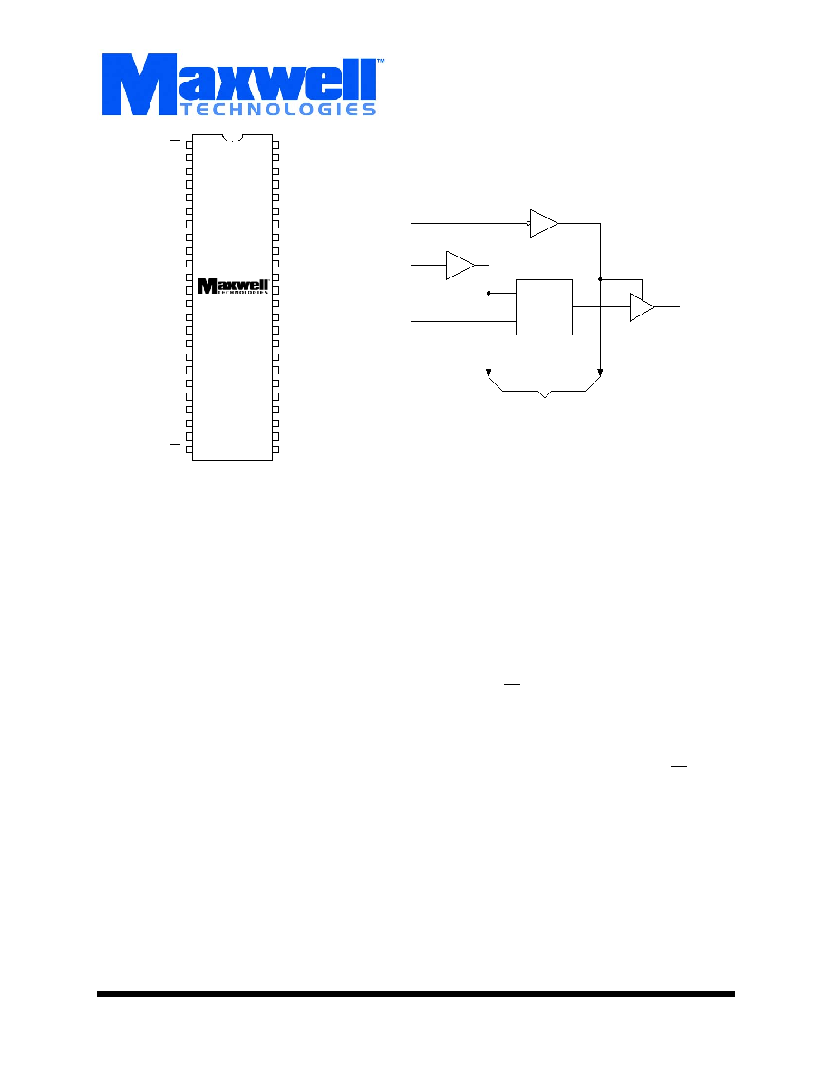
1
48
24
25
1LE
1D1
1D2
GND
1D3
1D4
VCC
1D5
1D6
GND
1D7
1D8
2D1
2D2
GND
2D3
2D4
VCC
2D5
2D6
GND
2D7
2D8
2LE
2OE
2Q8
2Q7
GND
2Q6
2Q5
VCC
2Q4
2Q3
GND
2Q2
2Q1
1Q8
1Q7
GND
1Q6
1Q5
VCC
1Q4
1Q3
GND
1Q2
1Q1
1OE
1OE/2OE
1LE/2LE
1D1/2D1
C1
1D
1/24
48/25
47/36
2/13
1Q1/2Q1
To Seven Other Channels
Logic Diagram (PositiveLogic)
54LVTH16373
Logic Diagram
Memory
P
RELIMINARY
2
All data sheets are subject to change without notice
©2001 Maxwell Technologies
All rights reserved.
3.3V ABT 16-Bit Transparent D-Type Latches
54LVTH16373
12.19.01 Rev 1
1000603
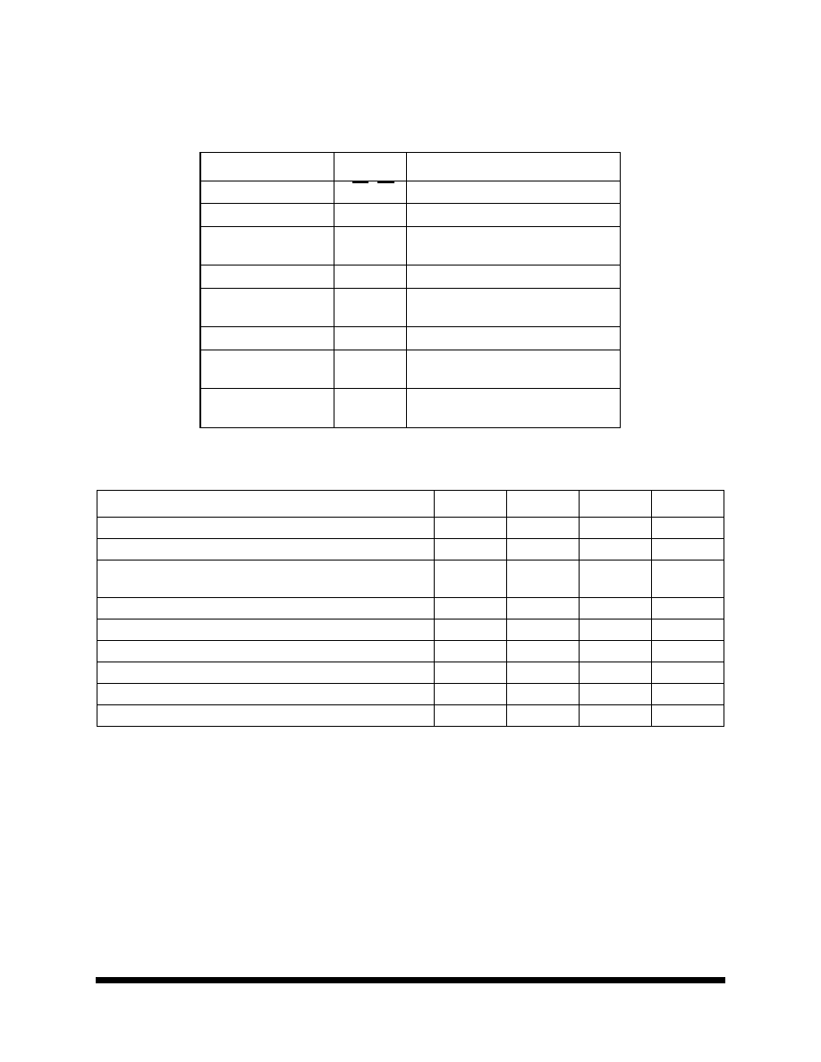
T
ABLE
1. P
INOUT
D
ESCRIPTION
P
IN
S
YMBOL
D
ESCRIPTION
1, 24
1OE-2OE
Output Enable
2, 3, 5, 6, 8, 9, 11, 12
1Q1-1Q8
Outputs
4, 10, 15, 21, 28, 34, 39,
45
GND
Ground
7, 31, 42
V
CC
Power Supply
13, 14, 16, 17, 19, 20, 22,
23
2Q1-2Q8
Outputs
25, 48
2LE-1LE
Latch Enable
26, 27, 29, 30, 32, 31, 32,
33, 35, 36
2D8-2D1
Inputs
37, 38, 40, 41, 43, 44, 46,
47
1D8-1D1
Inputs
T
ABLE
2. 54LVTH16373 A
BSOLUTE
M
AXIMUM
R
ATINGS
P
ARAMETER
S
YMBOL
M
IN
M
AX
U
NIT
Supply voltage range
V
CC
-0.5
4.6
V
Input voltage range
1
1. The input and output negative-voltage ratings may be exceeded if the input and output clamp-current ratings are observed.
V
I
-0.5
7
V
Voltage range applied to any output in the high state or power-off
state
1
V
O
-0.5
7
V
Current into any output in the low state
I
O
--
96
mA
Current into any output in the high state
2
2. This current flows only when the output is in the high state and V
O
> V
CC
.
I
O
--
48
mA
Input clamp current (V
I
< 0)
I
IK
--
-50
mA
Output clamp current (V
O
< O)
I
OK
--
-50
mA
Maximum power dissipation at TA = 55°C
3
3. The maximum package power dissipation is calculated using a junction temperature of 150
°
C and a board trace length of 750
mils.
P
D
--
0.85
mW
Storage temperature range
T
S
-65
150
°
C
Memory
P
RELIMINARY
3
All data sheets are subject to change without notice
©2001 Maxwell Technologies
All rights reserved.
3.3V ABT 16-Bit Transparent D-Type Latches
54LVTH16373
12.19.01 Rev 1
1000603
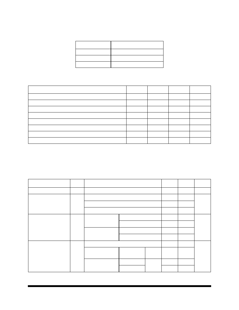
T
ABLE
3. D
ELTA
L
IMITS
P
ARAMETER
V
ARIATION
I
CC(OL)
±10% of specified value in Table 5
I
CC(OH)
±10% of specified value in Table 5
I
CC(OD)
±10% of specified value in Table 5
T
ABLE
4. 54LVTH16373 R
ECOMMENDED
O
PERATING
C
ONDITIONS
1
1. Unused control inputs must be held high or low to prevent them from floating.
P
ARAMETER
S
YMBOL
M
IN
M
AX
U
NIT
Supply voltage
V
CC
2.7
3.6
V
High-level input voltage
V
IH
2
--
V
Low-level input voltage
V
IL
--
0.8
V
Input voltage
V
I
--
5.5
V
High-level output current
I
OH
--
-24
mA
Low-level output current
I
OL
--
68
mA
Input transition rise or fall rate (outputs enabled)
t/
v
--
10
ns/V
Operating free-air temperature
T
A
-55
125
°
C
T
ABLE
5. 54LVTH16373 DC E
LECTRICAL
C
HARACTERISTICS
(V
CC
= 3.3V ±10%, T
A
= -55 to 125
°
C,
UNLESS
OTHERWISE
SPECIFIED
)
P
ARAMETER
S
YMBOL
T
EST
C
ONDITIONS
M
IN
M
AX
U
NIT
Input Clamp Voltage
V
IK
V
CC
= 2.7
I
I
= -18mA
--
-1.2
V
High-Level Output Voltage
V
OH
V
CC
= 2.7V to 3.6V
I
OH
= -100µA
V
CC
-0.2
--
V
V
CC
= 2.7V
I
OH
= -8mA
2.4
--
V
CC
= 3V,
I
OH
= -32mA
2.0
--
Low-Level Output Voltage
V
OL
V
CC
= 2.7V
I
OL
= 100µA
--
0.2
V
I
OL
= 24mA
--
0.5
V
CC
= 3V
I
OL
= 16mA
--
0.4
I
OL
= 32mA
--
0.5
Input Current
I
I
V
CC
= 0 or 3.6V
V
I
= 5.5V
10
µA
V
CC
= 3.6V
V
I
= V
CC
or GND Control
Inputs
--
±1
V
CC
= 3.6V
V
I
= V
CC
Data
Inputs
--
1
V
I
= 0
--
-5
Memory
P
RELIMINARY
4
All data sheets are subject to change without notice
©2001 Maxwell Technologies
All rights reserved.
3.3V ABT 16-Bit Transparent D-Type Latches
54LVTH16373
12.19.01 Rev 1
1000603
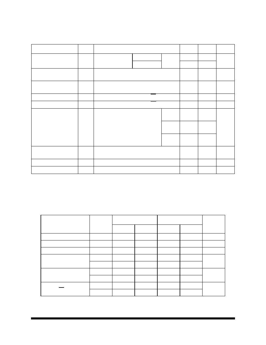
Hold Current
I
I(HOLD)
V
CC
= 3V
V
I
= 0.8V
Data
Inputs
75
--
µA
V
I
= 2V
-75
--
Output Disabled Leakage
Current - High
I
OZH
V
CC
= 3.6V, V
O
= 3V
--
5
µA
Output Disabled Leakage
Current - Low
I
OZL
V
CC
= 3.6V, V
O
= 0.5V
--
-5
µA
Power Up Current
I
OZPU
2
V
CC
= 0 to 1.5V, V
O
= 0.5V to 3V, OE = don't care
--
±100
µA
Power Down Current
I
OZPD
2
V
CC
= 1.5V to 0, V
O
= 0.5V to 3V, OE = don't care
--
±100
µA
Supply Current
I
CC
V
CC
= 3.6V
I
O
= 0
V
I
= V
CC
or GND
Outputs
high
--
0.19
mA
Outputs
low
--
5
Outputs
disabled
--
0.19
Delta Supply Current
I
CC
1
V
CC
= 3V to 3.6V, One input at V
CC
-0.6V, Other
inputs at V
CC
or GND
--
0.2
mA
Input Capacitance
C
I
2
V
I
= 3V or 0
--
10
pF
Input Output Capacitance
C
O
2
V
O
= 3V or 0
--
15
pF
1. This is the increase in supply current for each input that is at the specified TTL voltage level rather than V
CC
or GND.
2. Guaranteed by design.
T
ABLE
6. 54LVTH16373 AC E
LECTRICAL
C
HARACTERISTICS
(V
CC
= 3.3V ±10%, T
A
= -55 to 125
°
C,
UNLESS
OTHERWISE
SPECIFIED
)
P
ARAMETER
S
YMBOL
V
CC
= 3.3V ± 0.3V
V
CC
= 2.7V
U
NIT
M
IN
M
AX
M
IN
M
AX
Pulse duration, LE high
t
W
3.3
--
3.3
--
ns
Setup time, data before LEØ
t
SU
0.5
--
0.5
--
ns
Hold time, data after LEØ
t
H
1.8
--
2
--
ns
Propagation Delay Time
D to Q
t
PLH
2.7
5
--
5.7
ns
t
PHL
2.9
4.9
--
5.7
Propagation Delay Time
LE to Q
t
PLH
3.6
6
--
6.8
ns
t
PHL
4.7
6.9
--
8.8
Output Enable Time
OE to Q
t
PZH
2.9
5.3
--
6.3
ns
t
PZL
3
5.1
--
5.9
T
ABLE
5. 54LVTH16373 DC E
LECTRICAL
C
HARACTERISTICS
(V
CC
= 3.3V ±10%, T
A
= -55 to 125
°
C,
UNLESS
OTHERWISE
SPECIFIED
)
P
ARAMETER
S
YMBOL
T
EST
C
ONDITIONS
M
IN
M
AX
U
NIT
Memory
P
RELIMINARY
5
All data sheets are subject to change without notice
©2001 Maxwell Technologies
All rights reserved.
3.3V ABT 16-Bit Transparent D-Type Latches
54LVTH16373
12.19.01 Rev 1
1000603
F
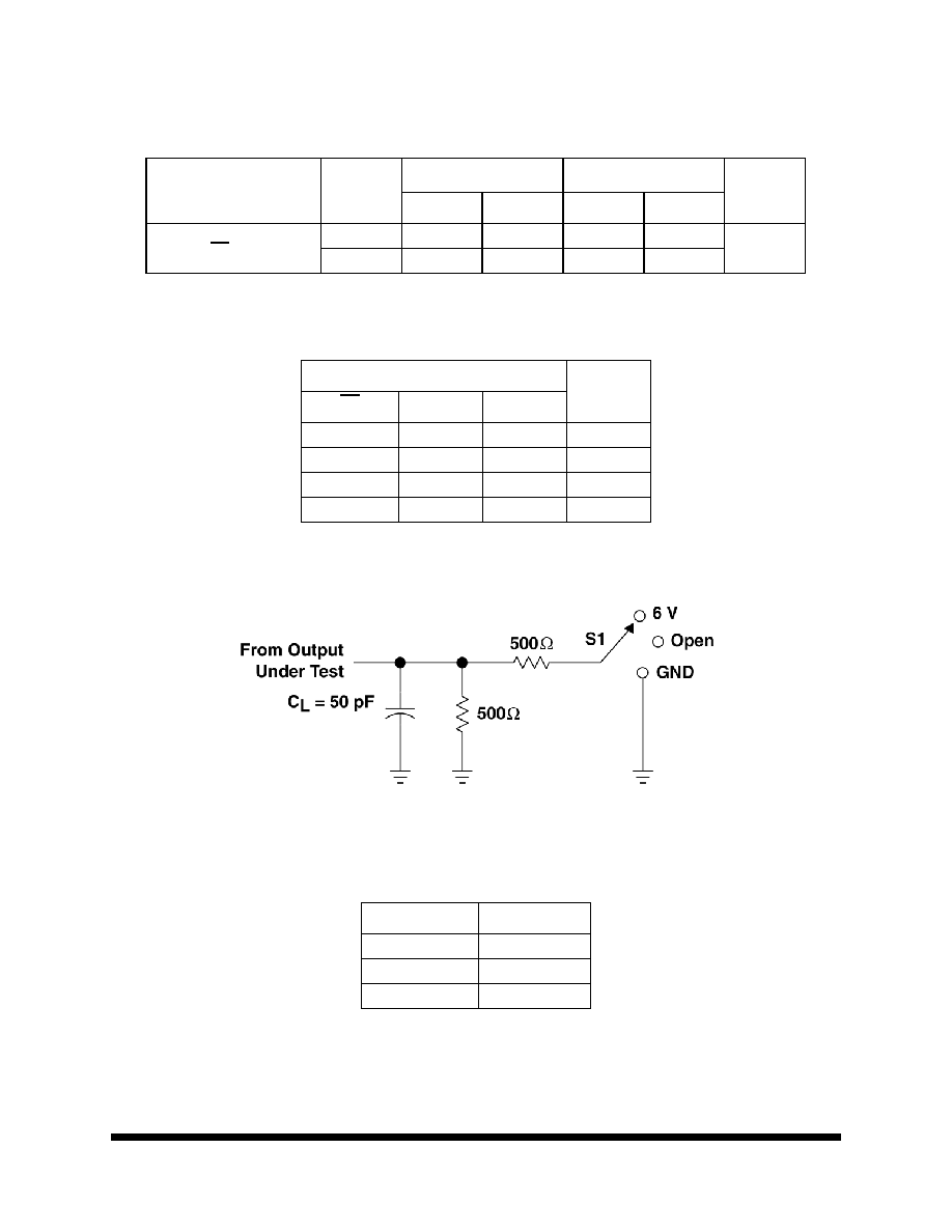
IGURE
1. L
OAD
C
IRCUIT
FOR
O
UTPUTS
Figure Note:
1. C
L
includes probe and jig capacitance.
Output Disable Time
OE to Q
t
PHZ
4.3
6.8
--
7.6
ns
t
PLZ
4
5.8
--
5.9
T
ABLE
7. F
UNCTION
T
ABLE
(
EACH
8-
BIT
SECTION
)
INPUTS
OUTPUT
Q
OE
LE
D
L
H
H
H
L
H
L
L
L
L
X
Q
0
H
X
X
Z
P
ARAMETER
M
EASUREMENT
I
NFORMATION
T
EST
S1
T
PLH
/T
PHL
Open
T
PLZ
/T
PZL
6V
T
PHZ
/T
PZH
GND
T
ABLE
6. 54LVTH16373 AC E
LECTRICAL
C
HARACTERISTICS
(V
CC
= 3.3V ±10%, T
A
= -55 to 125
°
C,
UNLESS
OTHERWISE
SPECIFIED
)
P
ARAMETER
S
YMBOL
V
CC
= 3.3V ± 0.3V
V
CC
= 2.7V
U
NIT
M
IN
M
AX
M
IN
M
AX