BAT54
THRU
BAT54S
250mWatt, 30Volt
Schottky Barrier Diode
SOT-23
Suggested Solder
Pad Layout
Features
∑
Low Forward Voltage
∑
Surface Mount device
∑
Very small conduction losses
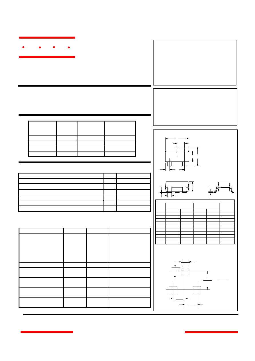
DIMENSIONS
INCHES
MM
DIM
MIN
MAX
MIN
MAX
NOTE
A
.110
.120
2.80
3.04
B
.083
.098
2.10
2.64
C
.047
.055
1.20
1.40
D
.035
.041
.89
1.03
E
.070
.081
1.78
2.05
F
.018
.024
.45
.60
G
.0005
.0039
.013
.100
H
.035
.044
.89
1.12
J
.003
.007
.085
.180
K
.015
.020
.37
.51
MCC
Catalog
Number
Device
Marking
Type
Pin
Configuration
Maximum Ratings
Continuos Reverse Voltage
V
R
30V
Electrical Characteristics @ 25
∞
C Unless Otherwise Specified
Ratings
Symbol
Max.
Notes
Forward Voltage at
I
F
= 0.1mA
I
F
= 1mA
I
F
= 10mA
I
F
= 30mA
I
F
= 100mA
V
F
240mV
320mV
400mV
500mV
900mV
Reverse Current
I
R
2.0 uA V
R
= 25V
Reverse Breakdown
Voltage
V
(BR)
>30V
Capacitance
C
J
10pF Measured at
1.0MHz, V
R
=1.0V
Reverse Recovery
Time
t
rr
5nS
I
F
=I
R
=10mA;
I
(REC)
= 1mA
Thermal Resistance,
Junction to Ambient
R
JA
500K/W
.079
2.000
inches
mm
.031
.800
.035
.900
.037
.950
.037
.950
A
B
C
D
E
F
G
H
J
K
www.
mccsemi
.com
Forward Current
I
F
0.3A
omponents
21201 Itasca Street Chatsworth
!"#
$
% !"#
M C C
Non-Repetitive Peak Forward Current t<1s
I
FSM
1.0mA
Total Power Dissipation @ T
A
= 25
∞
C P
D
250mW
Storage Temperature Range
T
stg
-55
∞
C to 150
∞
C
Junction Temperature
T
j
150
∞
C
BAT54 L4P Single Figure 1
BAT54A L42 Dual Figure 2
BAT54C L43 Dual Figure 3
BAT54S L44 Dual Figure 4
(See Page 3)
Soldering temperature during 10s T
j
260
∞
C
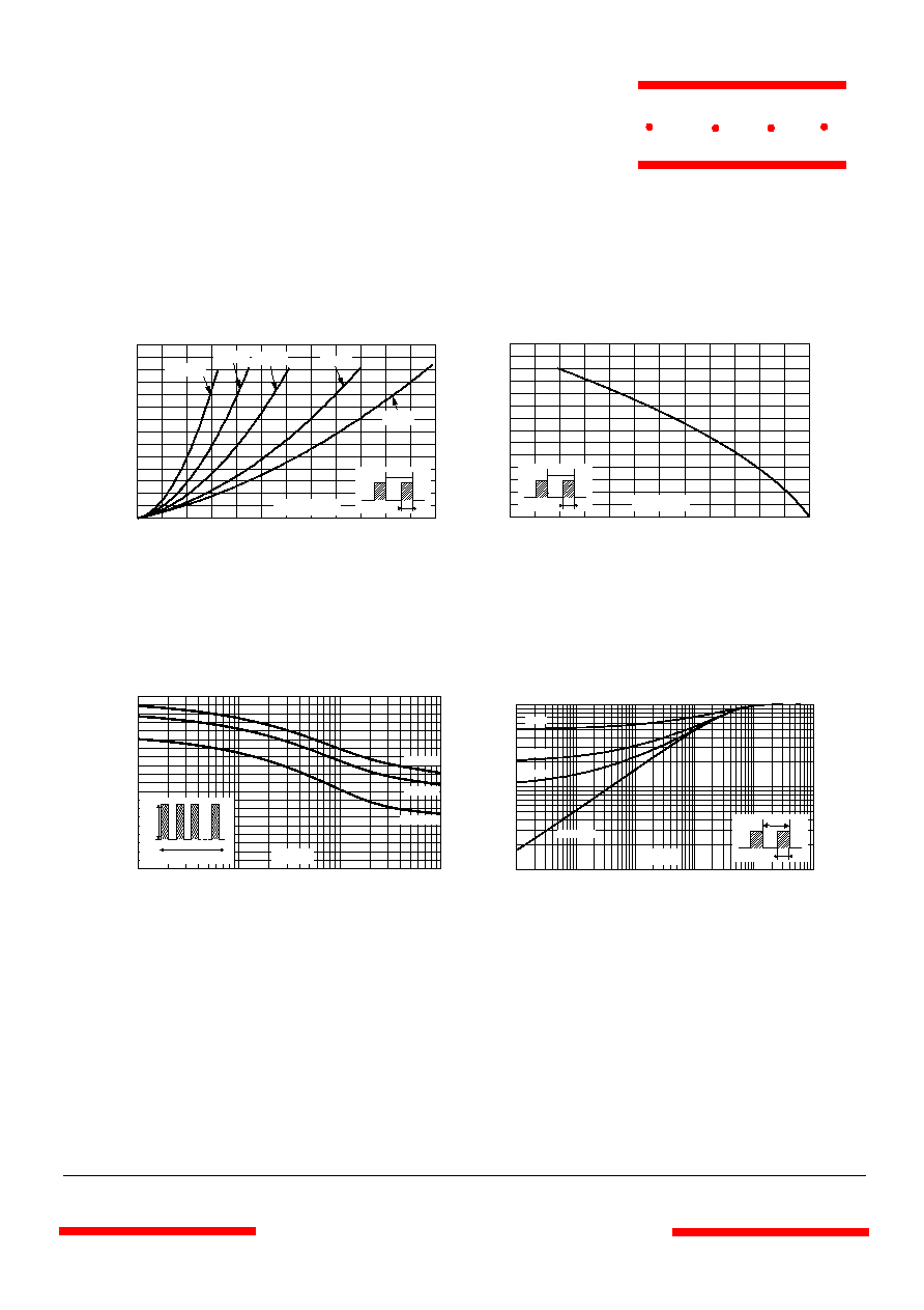
0.00
0.05
0.10
0.15
0.20
0.25
0.30
0.00
0.05
0.10
0.15
0.20
0.25
0.30
0.35
PF(av)(W)
= 0.2
= 0.5
= 1
= 0.05
= 0.1
IF(av) (A)
T
=tp/T
tp
Fig.1 : Average forward power dissipation versus
average forward current.
0
25
50
75
100
125
150
0.00
0.05
0.10
0.15
0.20
0.25
0.30
0.35
IF(av)(A)
T
=tp/T
tp
Tamb(∞C)
Fig.2 : Average forward current versus ambient
temperature (
= 1).
1E-3
1E-2
1E-1
1E+0
0.0
0.1
0.2
0.3
0.4
0.5
0.6
0.7
0.8
0.9
1.0
IM(A)
Ta=25∞C
Ta=50∞C
Ta=100∞C
I
M
t
=0.5
t(s)
Fig.3 : Non repetitive surge peak forward current
versus overload duration (maximum values).
1E-3
1E-2
1E-1
1E+0
1E+1
1E+2
0.01
0.10
1.00
tp(s)
Zth(j-a)/Rth(j-a)
T
=tp/T
tp
Single pulse
= 0.1
= 0.2
= 0.5
Fig.4 : Relative variation of thermal impedance
junction to ambient versus pulse duration (alumine
substrate 10mm x 8mm x 0.5mm).
www.
mccsemi
.com
BAT54 thru BAT54S
M C C

1
2
5
10
20
30
1
2
5
10
VR(V)
C(pF)
F=1MHz
Tj=25∞C
Fig.7 : Junction capacitance versus reverse
voltage applied (typical values).
0.0
0.1
0.2
0.3
0.4
0.5
0.6
0.7
0.8
0.9
1.0
1E-4
1E-3
1E-2
1E-1
5E-1
VFM(V)
IFM(A)
Tj=100∞C
Tj=50∞C
Tj=25∞C
Fig.8 : Forward voltage drop versus forward
current (typical values).
0
5
10
15
20
25
30
1E-2
1E-1
1E+0
1E+1
1E+2
VR(V)
IR(µA)
Tj=50∞C
Tj=25∞C
Tj=100∞C
Fig.5 : Reverse leakage current versus reverse
voltage applied (typical values).
0
25
50
75
100
125
150
1E-2
1E-1
1E+0
1E+1
1E+2
1E+3
1E+4
IR(µA)
VR=30V
Tj(∞C)
Fig.6 : Reverse leakage current versus junction
temperature.
www.
mccsemi
.com
BAT54 thru BAT54S
M C C
BAT54 BAT54A BAT54C BAT54S
Figure 1
Figure 2
Figure 3
Figure 4
Pin Configuration - Top View
1
2
3