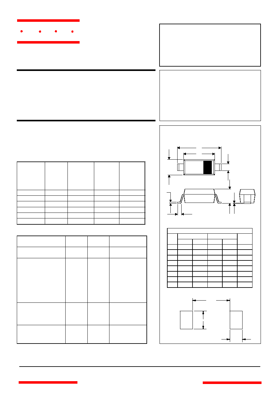
DIMENSIONS
INCHES
MM
DIM
MIN
MAX
MIN
MAX
NOTE
A
.140
.152
3.55
3.85
B
.100
.112
2.55
2.85
C
.055
.071
1.40
1.80
D
-----
.053
-----
1.35
E
.012
.031
0.30
.78
G
.006
-----
0.15
-----
H
-----
.01
-----
.25
J
-----
.006
-----
.15
Features
l
High Current Capability
l
Extremely Low Thermal Resistance
l
For Surface Mount Application
l
Higher Temp Soldering: 250
o
C for 10 Seconds At Terminals
l
Low Forward Voltage
Maximum Ratings
l
Operating Temperature: -55
o
C to +150
o
C
l
Storage Temperature: -55
o
C to +150
o
C
l
Maximum Thermal Resistance: 5
o
C/W Junction to Lead
MBR0520 R2 20V 14V 20V
MBR0530 R3 30V 21V 30V
MBR0540 R4 40V 28V 40V
MBR0560 R6 60V 42V 60V
MBR0580 R8 80V 56V 80V
MBR05100 RA 100V 70V 100V
Maximum
DC
Blocking
Voltage
MCC
Catalog
Number
Device
Marking
Maximum
Recurrent
Peak
Reverse
Voltage
Maximum
RMS
Voltage
Electrical Characteristics @ 25
o
C Unless Otherwise Specified
Average Forward
Current
I
F(AV)
0.5A
T
J
=115
o
C
Peak Forward Surge
Current
I
FSM
5.5A
8.3ms half sine
Maximum
Instantaneous
Forward Voltage
MBR0520
MBR0530
MBR0540
MBR0560
MBR0580-05100
V
F
0.45V
0.55V
0.55V
0.70V
0.80V
I
FM
=0.5A
T
A
=25
o
C
Maximum DC
Reverse Current At
Rated DC Blocking
Voltage
I
R
0.2mA T
J
=25
o
C
Typical Junction
Capacitance
C
J
30pF
Measured at
1.0MHz,
V
R
=4.0 V
MBR0520
THRU
MBR05100
0.5 Amp
Schottky Rectifier
20 to 100 Volts
0.036"
0.093"
0.048"
SUGGESTED SOLDER
PAD LAYOUT
A
B
E
C
J
D
H
G
SOD123
www.
mccsemi
.com
omponents
21201 Itasca Street Chatsworth
!"#
$
% !"#
M C C
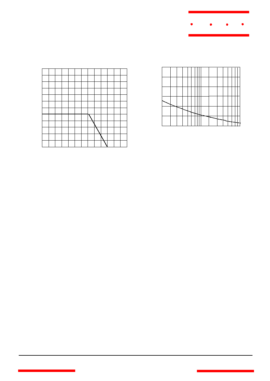
MBR0520 thru MBR05100
Average Forward Rectified Current - Amperes
versus
Ambient Temperature -
∞
C
Figure 3
Forward Derating Curve
0
175
50
75
100
125
0
.2
.4
.6
Single Phase, Half Wave
60Hz Resistive or Inductive Load
Amps
∞
C
150
.8
1.0
1.2
1
100
4
0
2
5
4
6
8
Figure 4
Peak Forward Surge Current
Peak Forward Surge Current - Amperes
versus
Number Of Cycles At 60Hz - Cycles
Amps
Cycles
2
6
10 20
60 80
40
8
10
12
M C C
www.
mccsemi
.com