Features
l
SOT-23 Package For surface mount application
l
Protects 3.0/3.3 up through 36V Components
l
Protects 2 Unidirectional or 1 Bidirectional line
l
Provides electrically isolated protection
l
Tape & Reel EIA Standard 481.
Mechanical Data
l
Molded: SOT-23 Surface Mount
l
Body marked with device number.
l
Mounting Position: Any
l
Weight: 0.14 grams (approx.)
MAXIMUM RATINGS
ß
Operating Temperature: -55
o
C to +150
o
C
ß
Storage Temperature: -55
o
C to +150
o
C
ß
SM03 thru SM36 have a Peak Pulse Power:500 Watts
(8/20 usec, Figure 1)
ß
Pulse Repetition Rate: <.01%
Packaging
SM03
THRU
SM36
Transient
Voltage Suppressor
500 Watt
SOT-23
Suggested Solder
Pad Layout
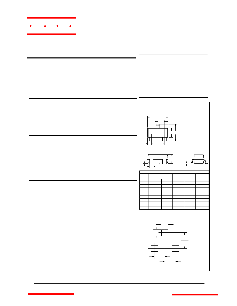
DIMENSIONS
INCHES
MM
DIM
MIN
MAX
MIN
MAX
NOTE
A
.110
.120
2.80
3.04
B
.083
.098
2.10
2.64
C
.047
.055
1.20
1.40
D
.035
.041
.89
1.03
E
.070
.081
1.78
2.05
F
.018
.024
.45
.60
G
.0005
.0039
.013
.100
H
.035
.044
.89
1.12
J
.003
.007
.085
.180
K
.015
.020
.37
.51
A
B
C
D
E
F
G
H
J
.079
2.000
inches
mm
.031
.800
.035
.900
.037
.950
.037
.950
www.
mccsemi
.com
The S
M03 thru SM36 product provides board level
protection from static electricity and other induced-voltage
surges that can damage sensitive circuitry.
These TRANSIENT VOLTAGE SUPPRESSOR (TVS)
Diode Arrays protect 3.0/3.3 Volt components such as
DRAM's, SRAM's, COMS, HCOMS, HSIC, and low volt.
interfaces up to
36 volts. Because of the physical size,
weight and protection capabilities, this product is ideal
for use in but not limited to miniaturized electronic
equipment such as hand held instruments, computers,
computer peripherals and cell phones.
omponents
21201 Itasca Street Chatsworth
!"#
$
% !"#
M C C

SM03 thru SM36
NOTE: Transient Voltage Suppression (TVS) product is normally selected based on its stand off Voltage V
WM
. Product
selected voltage should be equal to or greater than the continuous peak operating voltage of the circuit to be protected.
WAVE FORMS
MOUNTING PAD SOT23 CIRCUIT DIAGRAM
0 10 20 30
0
50
100
t -- Time in microsec
Ipp -- Peak Pulse Current -- % Ipp
Peak Value -- Ipp
Half-Value -- Ipp
2
8 X 20 Waveform
t
t
d
FIGURE 2
Pulse Wave Form
FIGURE 1
Peak Pulse Power Vs Pulse Time
ELECTRICAL CHARACTERISTICS PER LINE @ 25∫C Unless otherwise specified
STAND
OFF
VOLTAGE
V
WM
VOLTS
BREAKDOWN
VOLTAGE
V
BR
@1 mA
VOLTS
CLAMPING
VOLTAGE
V
C
@ 1 Amp
(FIGURE 2)
VOLTS
CLAMPING
VOLTAGE
V
C
@ 5 Amp
(FIGURE 2)
VOLTS
LEAKAGE
CURRENT
I
D
@ V
WM
µA
CAPACITANCE
@0V, 1 MHz
C
Pin 1-3 or 2-3
pF
CAPACITANCE
@0V, 1 MHz
C
Pin 1-2
pF
PART
NUMBER
DEVICE
MARKING
MIN MAX MAX MAX MAX MAX
SM03 M03 3.3 4 7 9 200 800 400
SM05 M05 5.0 6.0 9.8 11 100 600 300
SM12 M12 12.0 13.3 19 24 1 185 93
SM15 M15 15.0 16.7 24 30 1 140 70
SM24 M24 24.0 26.7 43 55 1 88 44
SM36 M36 36.0 40.0 60 75 1 88 39
NOTE: Transient Voltage Suppression (TVS) product is normally selected based on its stand off Voltage V
WM
. Product
selected voltage should be equal to or greater than the continuous peak operating voltage of the circuit to be protected.
www.
mccsemi
.com
M C C