
1
P/N:PM1170
REV. 0.04, JUL. 11, 2005
MX29LA128M T/B
128M-BIT SINGLE VOLTAGE 3V ONLY
BOOT SECTOR FLASH MEMORY
FEATURES
GENERAL FEATURES
∑ Single Power Supply Operation
- 2.7 to 3.6 volt for read, erase, and program opera-
tions
∑ Configuration
- 16,777,216 x 8 / 8,388,608 x 16 switchable
∑ Sector structure
- 8KB(4KW) x 8 and 64KB(32KW) x 255
∑ Latch-up protected to 250mA from -1V to VCC + 1V
∑ Low VCC write inhibit is equal to or less than 1.5V
∑ Compatible with JEDEC standard
- Pin-out and software compatible to single power sup-
ply Flash
PERFORMANCE
∑ High Performance
- Fast access time: 90R/100ns
- Page read time: 25ns
- Sector erase time: 0.5s (typ.)
- 4 word/8 byte page read buffer
- 16 word/ 32 byte write buffer: reduces programming
time for multiple-word/byte updates
∑ Low Power Consumption
- Active read current: 18mA(typ.)
- Active write current: 20mA(typ.)
- Standby current: 20uA(typ.)
∑ Minimum 100,000 erase/program cycle
∑ 20-years data retention
SOFTWARE FEATURES
∑ Support Common Flash Interface (CFI)
- Flash device parameters stored on the device and
provide the host system to access.
∑ Program Suspend/Program Resume
- Suspend program operation to read other sectors
∑ Erase Suspend/ Erase Resume
- Suspends sector erase operation to read data/pro-
gram other sectors
∑ Status Reply
- Data# polling & Toggle bits provide detection of pro-
gram and erase operation completion
HARDWARE FEATURES
∑ Ready/Busy (RY/BY#) Output
- Provides a hardware method of detecting program
and erase operation completion
∑ Hardware Reset (RESET#) Input
- Provides a hardware method to reset the internal
state machine to read mode
∑ WP#/ACC input
- Write protect (WP#) function allows protection of all
sectors, regardless of sector protection settings
- ACC (high voltage) accelerates programming time
for higher throughput during system
SECURITY
∑ Sector Protection/Chip Unprotect
- Provides sector group protect function to prevent pro-
gram or erase operation in the protected sector group
- Provides chip unprotect function to allow code
changes
- Provides temporary sector group unprotect function
for code changes in previously protected sector groups
∑ Sector Permanent Lock
- A unique lock bit feature allows the content to be
permanently locked
(Please contact Macronix sales for specific infor-
mation regarding this permanent lock feature)
∑ Secured Silicon Sector
- Provides a 128-word OTP area for permanent, se-
cure identification
- Can be programmed and locked at factory or by cus-
tomer
PACKAGE
∑ 56-pin TSOP
GENERAL DESCRIPTION
The MX29LA128M T/B is a 128-mega bit Flash memory
organized as 16M bytes of 8 bits or 8M words of 16 bits.
MXIC's Flash memories offer the most cost-effective and
reliable read/write non-volatile random access memory.
The MX29LA128M T/B is packaged in 56-pin TSOP. It is
designed to be reprogrammed and erased in system or in
standard EPROM programmers.
The standard MX29LA128M T/B offers access time as
fast as 90ns, allowing operation of high-speed micropro-
cessors without wait states. To eliminate bus conten-
tion, the MX29LA128M T/B has separate chip enable
(CE#) and output enable (OE#) controls.
MXIC's Flash memories augment EPROM functionality
PRELIMINARY

2
P/N:PM1170
REV. 0.04, JUL. 11, 2005
MX29LA128M T/B
with in-circuit electrical erasure and programming. The
MX29LA128M T/B uses a command register to manage
this functionality.
MXIC Flash technology reliably stores memory contents
even after 100,000 erase and program cycles. The MXIC
cell is designed to optimize the erase and program
mechanisms. In addition, the combination of advanced
tunnel oxide processing and low internal electric fields
for erase and programming operations produces reliable
cycling. The MX29LA128M T/B uses a 2.7V to 3.6V
VCC supply to perform the High Reliability Erase and
auto Program/Erase algorithms.
The highest degree of latch-up protection is achieved
with MXIC's proprietary non-epi process. Latch-up pro-
tection is proved for stresses up to 100 milliamperes on
address and data pin from -1V to VCC + 1V.
AUTOMATIC PROGRAMMING
The MX29LA128M T/B is byte/word/page programmable
using the Automatic Programming algorithm. The Auto-
matic Programming algorithm makes the external sys-
tem do not need to have time out sequence nor to verify
the data programmed.
AUTOMATIC PROGRAMMING ALGORITHM
MXIC's Automatic Programming algorithm require the user
to only write program set-up commands (including 2 un-
lock write cycle and A0H) and a program command (pro-
gram data and address). The device automatically times
the programming pulse width, provides the program veri-
fication, and counts the number of sequences. A status
bit similar to DATA# polling and a status bit toggling be-
tween consecutive read cycles, provide feedback to the
user as to the status of the programming operation.
AUTOMATIC CHIP ERASE
The entire chip is bulk erased using 50 ms erase pulses
according to MXIC's Automatic Chip Erase algorithm. The
Automatic Erase algorithm automatically programs the
entire array prior to electrical erase. The timing and veri-
fication of electrical erase are controlled internally within
the device.
AUTOMATIC SECTOR ERASE
The MX29LA128M T/B is sector(s) erasable using MXIC's
Auto Sector Erase algorithm. Sector erase modes allow
sectors of the array to be erased in one erase cycle. The
Automatic Sector Erase algorithm automatically programs
the specified sector(s) prior to electrical erase. The tim-
ing and verification of electrical erase are controlled inter-
nally within the device.
AUTOMATIC ERASE ALGORITHM
MXIC's Automatic Erase algorithm requires the user to
write commands to the command register using stan-
dard microprocessor write timings. The device will auto-
matically pre-program and verify the entire array. Then
the device automatically times the erase pulse width,
provides the erase verification, and counts the number
of sequences. A status bit toggling between consecu-
tive read cycles provides feedback to the user as to the
status of the programming operation.
Register contents serve as inputs to an internal state-
machine which controls the erase and programming cir-
cuitry. During write cycles, the command register inter-
nally latches address and data needed for the program-
ming and erase operations. During a system write cycle,
addresses are latched on the falling edge, and data are
latched on the rising edge of WE# .
MXIC's Flash technology combines years of EPROM
experience to produce the highest levels of quality, reli-
ability, and cost effectiveness. The MX29LA128M T/B
electrically erases all bits simultaneously using Fowler-
Nordheim tunneling. The bytes are programmed by us-
ing the EPROM programming mechanism of hot elec-
tron injection.
During a program cycle, the state-machine will control
the program sequences and command register will not
respond to any command set. During a Sector Erase
cycle, the command register will only respond to Erase
Suspend command. After Erase Suspend is completed,
the device stays in read mode. After the state machine
has completed its task, it will allow the command regis-
ter to respond to its full command set.
3
P/N:PM1170
REV. 0.04, JUL. 11, 2005
MX29LA128M T/B
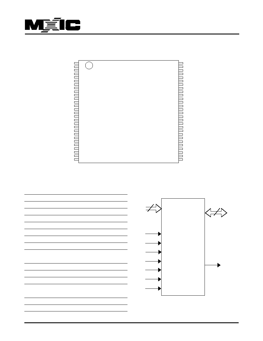
PIN CONFIGURATION
56 TSOP
SYMBOL
PIN NAME
A0~A22
Address Input
Q0~Q14
Data Inputs/Outputs
Q15/A-1
Q15(Word Mode)/LSB addr(Byte Mode)
CE#
Chip Enable Input
WE#
Write Enable Input
OE#
Output Enable Input
RESET#
Hardware Reset Pin, Active Low
WP#/ACC Hardware Write Protect/Programming
Acceleration input
RY/BY#
Read/Busy Output
BYTE#
Selects 8 bit or 16 bit mode
VCC
+3.0V single power supply
VI/O
Output Buffer Power (2.7V~3.6V this
input should be tied directly to VCC )
GND
Device Ground
NC
Pin Not Connected Internally
PIN DESCRIPTION
LOGIC SYMBOL
16 or 8
Q0-Q15
(A-1)
RY/BY#
A0-A22
CE#
OE#
WE#
RESET#
WP#/ACC
BYTE#
VI/O
23
NC
A22
A15
A14
A13
A12
A11
A10
A9
A8
A19
A20
WE#
RESET#
A21
WP#/ACC
RY/BY#
A18
A17
A7
A6
A5
A4
A3
A2
A1
NC
NC
1
2
3
4
5
6
7
8
9
10
11
12
13
14
15
16
17
18
19
20
21
22
23
24
25
26
27
28
NC
NC
A16
BYTE#
VSS
Q15/A-1
Q7
Q14
Q6
Q13
Q5
Q12
Q4
V
CC
Q11
Q3
Q10
Q2
Q9
Q1
Q8
Q0
OE#
VSS
CE#
A0
NC
VIO
56
55
54
53
52
51
50
49
48
47
46
45
44
43
42
41
40
39
38
37
36
35
34
33
32
31
30
29
4
P/N:PM1170
REV. 0.04, JUL. 11, 2005
MX29LA128M T/B
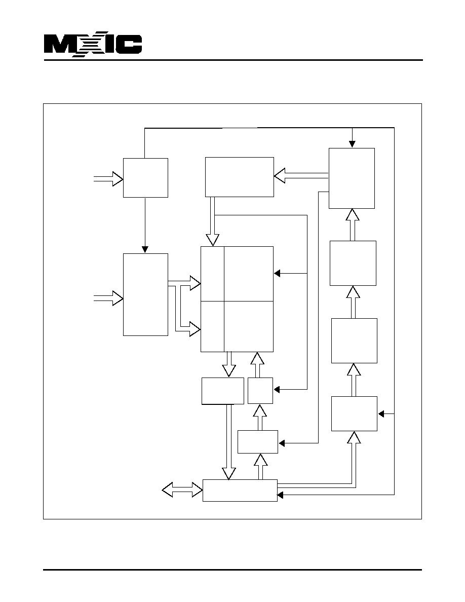
BLOCK DIAGRAM
CONTROL
INPUT
LOGIC
PROGRAM/ERASE
HIGH VOLTAGE
WRITE
STATE
MACHINE
(WSM)
STATE
REGISTER
FLASH
ARRAY
X-DECODER
ADDRESS
LATCH
AND
BUFFER
Y-PASS GATE
Y
-DECODER
ARRAY
SOURCE
HV
COMMAND
DATA
DECODER
COMMAND
DATA LATCH
I/O BUFFER
PGM
DATA
HV
PROGRAM
DATA LATCH
SENSE
AMPLIFIER
Q0-Q15/A-1
A0-A22
CE#
OE#
WE#
WP#
BYTE#
RESET#

5
P/N:PM1170
REV. 0.04, JUL. 11, 2005
MX29LA128M T/B
Sector
Sector
Sector Address
Sector Size
(x8)
(x16)
Group
A22-A12
(Kbytes/Kwords)
Address Range
Address Range
1
SA0
00000000xxx
64/32
000000-0FFFFF
000000-007FFF
1
SA1
00000001xxx
64/32
010000-1FFFFF
008000-00FFFF
1
SA2
00000010xxx
64/32
020000-2FFFFF
010000-017FFF
1
SA3
00000011xxx
64/32
030000-3FFFFF
018000-01FFFF
2
SA4
00000100xxx
64/32
040000-4FFFFF
020000-027FFF
2
SA5
00000101xxx
64/32
050000-5FFFFF
028000-02FFFF
2
SA6
00000110xxx
64/32
060000-6FFFFF
030000-037FFF
2
SA7
00000111xxx
64/32
070000-7FFFFF
038000-03FFFF
3
SA8
00001000xxx
64/32
080000-8FFFFF
040000-047FFF
3
SA9
00001001xxx
64/32
090000-9FFFFF
048000-04FFFF
3
SA10
00001010xxx
64/32
0A0000-AFFFFF
050000-057FFF
3
SA11
00001011xxx
64/32
0B0000-BFFFFF
058000-05FFFF
4
SA12
00001100xxx
64/32
0C0000-CFFFFF
060000-067FFF
4
SA13
00001101xxx
64/32
0D0000-DFFFFF
068000-06FFFF
4
SA14
00001110xxx
64/32
0E0000-EFFFFF
070000-077FFF
4
SA15
00001111xxx
64/32
0F0000-FFFFFF
078000-07FFFF
5
SA16
00010000xxx
64/32
100000-0FFFFF
080000-087FFF
5
SA17
00010001xxx
64/32
110000-1FFFFF
088000-08FFFF
5
SA18
00010010xxx
64/32
120000-2FFFFF
090000-097FFF
5
SA19
00010011xxx
64/32
130000-3FFFFF
098000-09FFFF
6
SA20
00010100xxx
64/32
140000-4FFFFF
0A0000-0A7FFF
6
SA21
00010101xxx
64/32
150000-5FFFFF
0A8000-0AFFFF
6
SA22
00010110xxx
64/32
160000-6FFFFF
0B0000-0B7FFF
6
SA23
00010111xxx
64/32
170000-7FFFFF
0B8000-0BFFFF
7
SA24
00011000xxx
64/32
180000-8FFFFF
0C0000-0C7FFF
7
SA25
00011001xxx
64/32
190000-9FFFFF
0C8000-0CFFFF
7
SA26
00011010xxx
64/32
1A0000-AFFFFF
0D0000-0D7FFF
7
SA27
00011011xxx
64/32
1B0000-BFFFFF
0D8000-0DFFFF
8
SA28
00011100xxx
64/32
1C0000-CFFFFF
0E0000-0E7FFF
8
SA29
00011101xxx
64/32
1D0000-DFFFFF
0E8000-0EFFFF
8
SA30
00011110xxx
64/32
1E0000-EFFFFF
0F0000-0F7FFF
8
SA31
00011111xxx
64/32
1F0000-FFFFFF
0F8000-0FFFFF
9
SA32
00100000xxx
64/32
200000-0FFFFF
100000-107FFF
9
SA33
00100001xxx
64/32
210000-1FFFFF
108000-10FFFF
9
SA34
00100010xxx
64/32
220000-2FFFFF
110000-117FFF
9
SA35
00100011xxx
64/32
230000-3FFFFF
118000-11FFFF
10
SA36
00100100xxx
64/32
240000-4FFFFF
120000-127FFF
10
SA37
00100101xxx
64/32
250000-5FFFFF
128000-12FFFF
10
SA38
00100110xxx
64/32
260000-6FFFFF
130000-137FFF
MX29LA128MT SECTOR ADDRESS TABLE

6
P/N:PM1170
REV. 0.04, JUL. 11, 2005
MX29LA128M T/B
Sector
Sector
Sector Address
Sector Size
(x8)
(x16)
Group
A22-A12
(Kbytes/Kwords)
Address Range
Address Range
10
SA39
00100111xxx
64/32
270000-7FFFFF
138000-13FFFF
11
SA40
00101000xxx
64/32
280000-8FFFFF
140000-147FFF
11
SA41
00101001xxx
64/32
290000-9FFFFF
148000-14FFFF
11
SA42
00101010xxx
64/32
2A0000-AFFFFF
150000-157FFF
11
SA43
00101011xxx
64/32
2B0000-BFFFFF
158000-15FFFF
12
SA44
00101100xxx
64/32
2C0000-CFFFFF
160000-167FFF
12
SA45
00101101xxx
64/32
2D0000-DFFFFF
168000-16FFFF
12
SA46
00101110xxx
64/32
2E0000-EFFFFF
170000-177FFF
12
SA47
00101111xxx
64/32
2F0000-FFFFFF
178000-17FFFF
13
SA48
00110000xxx
64/32
300000-0FFFFF
180000-187FFF
13
SA49
00110001xxx
64/32
310000-1FFFFF
188000-18FFFF
13
SA50
00110010xxx
64/32
320000-2FFFFF
190000-197FFF
13
SA51
00110011xxx
64/32
330000-3FFFFF
198000-19FFFF
14
SA52
00110100xxx
64/32
340000-4FFFFF
1A0000-1A7FFF
14
SA53
00110101xxx
64/32
350000-5FFFFF
1A8000-1AFFFF
14
SA54
00110110xxx
64/32
360000-6FFFFF
1B0000-1B7FFF
14
SA55
00110111xxx
64/32
370000-7FFFFF
1B8000-1BFFFF
15
SA56
00111000xxx
64/32
380000-8FFFFF
1C0000-1C7FFF
15
SA57
00111001xxx
64/32
390000-9FFFFF
1C8000-1CFFFF
15
SA58
00111010xxx
64/32
3A0000-AFFFFF
1D0000-1D7FFF
15
SA59
00111011xxx
64/32
3B0000-BFFFFF
1D8000-1DFFFF
16
SA60
00111100xxx
64/32
3C0000-CFFFFF
1E0000-1E7FFF
16
SA61
00111101xxx
64/32
3D0000-DFFFFF
1E8000-1EFFFF
16
SA62
00111110xxx
64/32
3E0000-EFFFFF
1F0000-1F7FFF
16
SA63
00111111xxx
64/32
3F0000-FFFFFF
1F8000-1FFFFF
17
SA64
01000000xxx
64/32
400000-0FFFFF
200000-207FFF
17
SA65
01000001xxx
64/32
410000-1FFFFF
208000-20FFFF
17
SA66
01000010xxx
64/32
420000-2FFFFF
210000-217FFF
17
SA67
01000011xxx
64/32
430000-3FFFFF
218000-21FFFF
18
SA68
01000100xxx
64/32
440000-4FFFFF
220000-227FFF
18
SA69
01000101xxx
64/32
450000-5FFFFF
228000-22FFFF
18
SA70
01000110xxx
64/32
460000-6FFFFF
230000-237FFF
18
SA71
01000111xxx
64/32
470000-7FFFFF
238000-23FFFF
19
SA72
01001000xxx
64/32
480000-8FFFFF
240000-247FFF
19
SA73
01001001xxx
64/32
490000-9FFFFF
248000-24FFFF
19
SA74
01001010xxx
64/32
4A0000-AFFFFF
250000-257FFF
19
SA75
01001011xxx
64/32
4B0000-BFFFFF
258000-25FFFF
20
SA76
01001100xxx
64/32
4C0000-CFFFFF
260000-267FFF
20
SA77
01001101xxx
64/32
4D0000-DFFFFF
268000-26FFFF
20
SA78
01001110xxx
64/32
4E0000-EFFFFF
270000-277FFF
20
SA79
01001111xxx
64/32
4F0000-FFFFFF
278000-27FFFF

7
P/N:PM1170
REV. 0.04, JUL. 11, 2005
MX29LA128M T/B
Sector
Sector
Sector Address
Sector Size
(x8)
(x16)
Group
A22-A12
(Kbytes/Kwords)
Address Range
Address Range
21
SA80
01010000xxx
64/32
500000-0FFFFF
280000-287FFF
21
SA81
01010001xxx
64/32
510000-1FFFFF
288000-28FFFF
21
SA82
01010010xxx
64/32
520000-2FFFFF
290000-297FFF
21
SA83
01010011xxx
64/32
530000-3FFFFF
298000-29FFFF
22
SA84
01010100xxx
64/32
540000-4FFFFF
2A0000-2A7FFF
22
SA85
01010101xxx
64/32
550000-5FFFFF
2A8000-2AFFFF
22
SA86
01010110xxx
64/32
560000-6FFFFF
2B0000-2B7FFF
22
SA87
01010111xxx
64/32
570000-7FFFFF
2B8000-2BFFFF
23
SA88
01011000xxx
64/32
580000-8FFFFF
2C0000-2C7FFF
23
SA89
01011001xxx
64/32
590000-9FFFFF
2C8000-2CFFFF
23
SA90
01011010xxx
64/32
5A0000-AFFFFF
2D0000-2D7FFF
23
SA91
01011011xxx
64/32
5B0000-BFFFFF
2D8000-2DFFFF
24
SA92
01011100xxx
64/32
5C0000-CFFFFF
2E0000-2E7FFF
24
SA93
01011101xxx
64/32
5D0000-DFFFFF
2E8000-2EFFFF
24
SA94
01011110xxx
64/32
5E0000-EFFFFF
2F0000-2F7FFF
24
SA95
01011111xxx
64/32
5F0000-FFFFFF
2F8000-2FFFFF
25
SA96
01100000xxx
64/32
600000-0FFFFF
300000-307FFF
25
SA97
01100001xxx
64/32
610000-1FFFFF
308000-30FFFF
25
SA98
01100010xxx
64/32
620000-2FFFFF
310000-317FFF
25
SA99
01100011xxx
64/32
630000-3FFFFF
318000-31FFFF
26
SA100
01100100xxx
64/32
640000-4FFFFF
320000-327FFF
26
SA101
01100101xxx
64/32
650000-5FFFFF
328000-32FFFF
26
SA102
01100110xxx
64/32
660000-6FFFFF
330000-337FFF
26
SA103
01100111xxx
64/32
670000-7FFFFF
338000-33FFFF
27
SA104
01101000xxx
64/32
680000-8FFFFF
340000-347FFF
27
SA105
01101001xxx
64/32
690000-9FFFFF
348000-34FFFF
27
SA106
01101010xxx
64/32
6A0000-AFFFFF
350000-357FFF
27
SA107
01101011xxx
64/32
6B0000-BFFFFF
358000-35FFFF
28
SA108
01101100xxx
64/32
6C0000-CFFFFF
360000-367FFF
28
SA109
01101101xxx
64/32
6D0000-DFFFFF
368000-36FFFF
28
SA110
01101110xxx
64/32
6E0000-EFFFFF
370000-377FFF
28
SA111
01101111xxx
64/32
6F0000-FFFFFF
378000-37FFFF
29
SA112
01110000xxx
64/32
700000-0FFFFF
380000-387FFF
29
SA113
01110001xxx
64/32
710000-1FFFFF
388000-38FFFF
29
SA114
01110010xxx
64/32
720000-2FFFFF
390000-397FFF
29
SA115
01110011xxx
64/32
730000-3FFFFF
398000-39FFFF
30
SA116
01110100xxx
64/32
740000-4FFFFF
3A0000-3A7FFF
30
SA117
01110101xxx
64/32
750000-5FFFFF
3A8000-3AFFFF
30
SA118
01110110xxx
64/32
760000-6FFFFF
3B0000-3B7FFF
30
SA119
01110111xxx
64/32
770000-7FFFFF
3B8000-3BFFFF
31
SA120
01111000xxx
64/32
780000-8FFFFF
3C0000-3C7FFF

8
P/N:PM1170
REV. 0.04, JUL. 11, 2005
MX29LA128M T/B
Sector
Sector
Sector Address
Sector Size
(x8)
(x16)
Group
A22-A12
(Kbytes/Kwords)
Address Range
Address Range
31
SA121
01111001xxx
64/32
790000-9FFFFF
3C8000-3CFFFF
31
SA122
01111010xxx
64/32
7A0000-AFFFFF
3D0000-3D7FFF
31
SA123
01111011xxx
64/32
7B0000-BFFFFF
3D8000-3DFFFF
32
SA124
01111100xxx
64/32
7C0000-CFFFFF
3E0000-3E7FFF
32
SA125
01111101xxx
64/32
7D0000-DFFFFF
3E8000-3EFFFF
32
SA126
01111110xxx
64/32
7E0000-EFFFFF
3F0000-3F7FFF
32
SA127
01111111xxx
64/32
7F0000-FFFFFF
3F8000-3FFFFF
33
SA128
10000000xxx
64/32
800000-0FFFFF
400000-407FFF
33
SA129
10000001xxx
64/32
810000-1FFFFF
408000-40FFFF
33
SA130
10000010xxx
64/32
820000-2FFFFF
410000-417FFF
33
SA131
10000011xxx
64/32
830000-3FFFFF
418000-41FFFF
34
SA132
10000100xxx
64/32
840000-4FFFFF
420000-427FFF
34
SA133
10000101xxx
64/32
850000-5FFFFF
428000-42FFFF
34
SA134
10000110xxx
64/32
860000-6FFFFF
430000-437FFF
34
SA135
10000111xxx
64/32
870000-7FFFFF
438000-43FFFF
35
SA136
10001000xxx
64/32
880000-8FFFFF
440000-447FFF
35
SA137
10001001xxx
64/32
890000-9FFFFF
448000-44FFFF
35
SA138
10001010xxx
64/32
8A0000-AFFFFF
450000-457FFF
35
SA139
10001011xxx
64/32
8B0000-BFFFFF
458000-45FFFF
36
SA140
10001100xxx
64/32
8C0000-CFFFFF
460000-467FFF
36
SA141
10001101xxx
64/32
8D0000-DFFFFF
468000-46FFFF
36
SA142
10001110xxx
64/32
8E0000-EFFFFF
470000-477FFF
36
SA143
10001111xxx
64/32
8F0000-FFFFFF
478000-47FFFF
37
SA144
10010000xxx
64/32
900000-0FFFFF
480000-487FFF
37
SA145
10010001xxx
64/32
910000-1FFFFF
488000-48FFFF
37
SA146
10010010xxx
64/32
920000-2FFFFF
490000-497FFF
37
SA147
10010011xxx
64/32
930000-3FFFFF
498000-49FFFF
38
SA148
10010100xxx
64/32
940000-4FFFFF
4A0000-4A7FFF
38
SA149
10010101xxx
64/32
950000-5FFFFF
4A8000-4AFFFF
38
SA150
10010110xxx
64/32
960000-6FFFFF
4B0000-4B7FFF
38
SA151
10010111xxx
64/32
970000-7FFFFF
4B8000-4BFFFF
39
SA152
10011000xxx
64/32
980000-8FFFFF
4C0000-4C7FFF
39
SA153
10011001xxx
64/32
990000-9FFFFF
4C8000-4CFFFF
39
SA154
10011010xxx
64/32
9A0000-AFFFFF
4D0000-4D7FFF
39
SA155
10011011xxx
64/32
9B0000-BFFFFF
4D8000-4DFFFF
40
SA156
10011100xxx
64/32
9C0000-CFFFFF
4E0000-4E7FFF
40
SA157
10011101xxx
64/32
9D0000-DFFFFF
4E8000-4EFFFF
40
SA158
10011110xxx
64/32
9E0000-EFFFFF
4F0000-4F7FFF
40
SA159
10011111xxx
64/32
9F0000-FFFFFF
4F8000-4FFFFF
41
SA160
10100000xxx
64/32
A00000-0FFFFF
500000-507FFF
41
SA161
10100001xxx
64/32
A10000-1FFFFF
508000-50FFFF

9
P/N:PM1170
REV. 0.04, JUL. 11, 2005
MX29LA128M T/B
Sector
Sector
Sector Address
Sector Size
(x8)
(x16)
Group
A22-A12
(Kbytes/Kwords)
Address Range
Address Range
41
SA162
10100010xxx
64/32
A20000-2FFFFF
510000-517FFF
41
SA163
10100011xxx
64/32
A30000-3FFFFF
518000-51FFFF
42
SA164
10100100xxx
64/32
A40000-4FFFFF
520000-527FFF
42
SA165
10100101xxx
64/32
A50000-5FFFFF
528000-52FFFF
42
SA166
10100110xxx
64/32
A60000-6FFFFF
530000-537FFF
42
SA167
10100111xxx
64/32
A70000-7FFFFF
538000-53FFFF
43
SA168
10101000xxx
64/32
A80000-8FFFFF
540000-547FFF
43
SA169
10101001xxx
64/32
A90000-9FFFFF
548000-54FFFF
43
SA170
10101010xxx
64/32
AA0000-AFFFFF
550000-557FFF
43
SA171
10101011xxx
64/32
AB0000-BFFFFF
558000-55FFFF
44
SA172
10101100xxx
64/32
AC0000-CFFFFF
560000-567FFF
44
SA173
10101101xxx
64/32
AD0000-DFFFFF
568000-56FFFF
44
SA174
10101110xxx
64/32
AE0000-EFFFFF
570000-577FFF
44
SA175
10101111xxx
64/32
AF0000-FFFFFF
578000-57FFFF
45
SA176
10110000xxx
64/32
B00000-0FFFFF
580000-587FFF
45
SA177
10110001xxx
64/32
B10000-1FFFFF
588000-58FFFF
45
SA178
10110010xxx
64/32
B20000-2FFFFF
590000-597FFF
45
SA179
10110011xxx
64/32
B30000-3FFFFF
598000-59FFFF
46
SA180
10110100xxx
64/32
B40000-4FFFFF
5A0000-5A7FFF
46
SA181
10110101xxx
64/32
B50000-5FFFFF
5A8000-5AFFFF
46
SA182
10110110xxx
64/32
B60000-6FFFFF
5B0000-5B7FFF
46
SA183
10110111xxx
64/32
B70000-7FFFFF
5B8000-5BFFFF
47
SA184
10111000xxx
64/32
B80000-8FFFFF
5C0000-5C7FFF
47
SA185
10111001xxx
64/32
B90000-9FFFFF
5C8000-5CFFFF
47
SA186
10111010xxx
64/32
BA0000-AFFFFF
5D0000-5D7FFF
47
SA187
10111011xxx
64/32
BB0000-BFFFFF
5D8000-5DFFFF
48
SA188
10111100xxx
64/32
BC0000-CFFFFF
5E0000-5E7FFF
48
SA189
10111101xxx
64/32
BD0000-DFFFFF
5E8000-5EFFFF
48
SA190
10111110xxx
64/32
BE0000-EFFFFF
5F0000-5F7FFF
48
SA191
10111111xxx
64/32
BF0000-FFFFFF
5F8000-5FFFFF
49
SA192
11000000xxx
64/32
C00000-0FFFFF
600000-607FFF
49
SA193
11000001xxx
64/32
C10000-1FFFFF
608000-60FFFF
49
SA194
11000010xxx
64/32
C20000-2FFFFF
610000-617FFF
49
SA195
11000011xxx
64/32
C30000-3FFFFF
618000-61FFFF
50
SA196
11000100xxx
64/32
C40000-4FFFFF
620000-627FFF
50
SA197
11000101xxx
64/32
C50000-5FFFFF
628000-62FFFF
50
SA198
11000110xxx
64/32
C60000-6FFFFF
630000-637FFF
50
SA199
11000111xxx
64/32
C70000-7FFFFF
638000-63FFFF
51
SA200
11001000xxx
64/32
C80000-8FFFFF
640000-647FFF
51
SA201
11001001xxx
64/32
C90000-9FFFFF
648000-64FFFF
51
SA202
11001010xxx
64/32
CA0000-AFFFFF
650000-657FFF
10
P/N:PM1170
REV. 0.04, JUL. 11, 2005
MX29LA128M T/B
Sector
Sector
Sector Address
Sector Size
(x8)
(x16)
Group
A22-A12
(Kbytes/Kwords)
Address Range
Address Range
51
SA203
11001011xxx
64/32
CB0000-BFFFFF
658000-65FFFF
52
SA204
11001100xxx
64/32
CC0000-CFFFFF
660000-667FFF
52
SA205
11001101xxx
64/32
CD0000-DFFFFF
668000-66FFFF
52
SA206
11001110xxx
64/32
CE0000-EFFFFF
670000-677FFF
52
SA207
11001111xxx
64/32
CF0000-FFFFFF
678000-67FFFF
53
SA208
11010000xxx
64/32
D00000-0FFFFF
680000-687FFF
53
SA209
11010001xxx
64/32
D10000-1FFFFF
688000-68FFFF
53
SA210
11010010xxx
64/32
D20000-2FFFFF
690000-697FFF
53
SA211
11010011xxx
64/32
D30000-3FFFFF
698000-69FFFF
54
SA212
11010100xxx
64/32
D40000-4FFFFF
6A0000-6A7FFF
54
SA213
11010101xxx
64/32
D50000-5FFFFF
6A8000-6AFFFF
54
SA214
11010110xxx
64/32
D60000-6FFFFF
6B0000-6B7FFF
54
SA215
11010111xxx
64/32
D70000-7FFFFF
6B8000-6BFFFF
55
SA216
11011000xxx
64/32
D80000-8FFFFF
6C0000-6C7FFF
55
SA217
11011001xxx
64/32
D90000-9FFFFF
6C8000-6CFFFF
55
SA218
11011010xxx
64/32
DA0000-AFFFFF
6D0000-6D7FFF
55
SA219
11011011xxx
64/32
DB0000-BFFFFF
6D8000-6DFFFF
56
SA220
11011100xxx
64/32
DC0000-CFFFFF
6E0000-6E7FFF
56
SA221
11011101xxx
64/32
DD0000-DFFFFF
6E8000-6EFFFF
56
SA222
11011110xxx
64/32
DE0000-EFFFFF
6F0000-6F7FFF
56
SA223
11011111xxx
64/32
DF0000-FFFFFF
6F8000-6FFFFF
57
SA224
11100000xxx
64/32
E00000-0FFFFF
700000-707FFF
57
SA225
11100001xxx
64/32
E10000-1FFFFF
708000-70FFFF
57
SA226
11100010xxx
64/32
E20000-2FFFFF
710000-717FFF
57
SA227
11100011xxx
64/32
E30000-3FFFFF
718000-71FFFF
58
SA228
11100100xxx
64/32
E40000-4FFFFF
720000-727FFF
58
SA229
11100101xxx
64/32
E50000-5FFFFF
728000-72FFFF
58
SA230
11100110xxx
64/32
E60000-6FFFFF
730000-737FFF
58
SA231
11100111xxx
64/32
E70000-7FFFFF
738000-73FFFF
59
SA232
11101000xxx
64/32
E80000-8FFFFF
740000-747FFF
59
SA233
11101001xxx
64/32
E90000-9FFFFF
748000-74FFFF
59
SA234
11101010xxx
64/32
EA0000-AFFFFF
750000-757FFF
59
SA235
11101011xxx
64/32
EB0000-BFFFFF
758000-75FFFF
60
SA236
11101100xxx
64/32
EC0000-CFFFFF
760000-767FFF
60
SA237
11101101xxx
64/32
ED0000-DFFFFF
768000-76FFFF
60
SA238
11101110xxx
64/32
EE0000-EFFFFF
770000-777FFF
60
SA239
11101111xxx
64/32
EF0000-FFFFFF
778000-77FFFF
61
SA240
11110000xxx
64/32
F00000-0FFFFFF
780000-787FFF
11
P/N:PM1170
REV. 0.04, JUL. 11, 2005
MX29LA128M T/B
Sector
Sector
Sector Address
Sector Size
(x8)
(x16)
Group
A22-A12
(Kbytes/Kwords)
Address Range
Address Range
61
SA241
11110001xxx
64/32
F10000-1FFFFF
788000-78FFFF
61
SA242
11110010xxx
64/32
F20000-2FFFFF
790000-797FFF
61
SA243
11110011xxx
64/32
F30000-3FFFFF
798000-79FFFF
62
SA244
11110100xxx
64/32
F40000-4FFFFF
7A0000-7A7FFF
62
SA245
11110101xxx
64/32
F50000-5FFFFF
7A8000-7AFFFF
62
SA246
11110110xxx
64/32
F60000-6FFFFF
7B0000-7B7FFF
62
SA247
11110111xxx
64/32
F70000-7FFFFF
7B8000-7BFFFF
63
SA248
11111000xxx
64/32
F80000-8FFFFF
7C0000-7C7FFF
63
SA249
11111001xxx
64/32
F90000-9FFFFF
7C8000-7CFFFF
63
SA250
11111010xxx
64/32
FA0000-AFFFFF
7D0000-7D7FFF
63
SA251
11111011xxx
64/32
FB0000-BFFFFF
7D8000-7DFFFF
64
SA252
11111100xxx
64/32
FC0000-CFFFFF
7E0000-7E7FFF
64
SA253
11111101xxx
64/32
FD0000-DFFFFF
7E8000-7EFFFF
64
SA254
11111110xxx
64/32
FE0000-EFFFFF
7F0000-7F7FFF
65
SA255
11111111000
8/4
FF0000-FF1FFF
7F8000-7F8FFF
66
SA256
11111111001
8/4
FF2000-FF3FFF
7F9000-7F9FFF
67
SA257
11111111010
8/4
FF4000-FF5FFF
7FA000-7FAFFF
68
SA258
11111111011
8/4
FF6000-FF7FFF
7FB000-7FBFFF
69
SA259
11111111100
8/4
FF8000-FF9FFF
7FC000-7FCFFF
70
SA260
11111111101
8/4
FFA000-FFBFFF
7FD000-7FDFFF
71
SA261
11111111110
8/4
FFC000-FFDFFF
7FE000-7FEFFF
72
SA262
11111111111
8/4
FFE000-FFFFFF
7FF000-7FFFFF
12
P/N:PM1170
REV. 0.04, JUL. 11, 2005
MX29LA128M T/B
Sector
Sector
Sector Address
Sector Size
(x8)
(x16)
Group
A22-A12
(Kbytes/Kwords)
Address Range
Address Range
1
SA0
00000000000
8/4
000000-001FFF
000000-000FFF
2
SA1
00000000001
8/4
002000-003FFF
001000-001FFF
3
SA2
00000000010
8/4
004000-005FFF
002000-002FFF
4
SA3
00000000011
8/4
006000-007FFF
003000-003FFF
5
SA4
00000000100
8/4
008000-009FFF
004000-004FFF
6
SA5
00000000101
8/4
00A000-00BFFF
005000-005FFF
7
SA6
00000000110
8/4
00C000-00DFFF
006000-006FFF
8
SA7
00000000111
8/4
00E000-00FFFF
007000-007FFF
9
SA8
00000001xxx
64/32
010000-1FFFFF
008000-00FFFF
9
SA9
00000010xxx
64/32
020000-2FFFFF
010000-017FFF
9
SA10
00000011xxx
64/32
030000-3FFFFF
018000-01FFFF
10
SA11
00000100xxx
64/32
040000-4FFFFF
020000-027FFF
10
SA12
00000101xxx
64/32
050000-5FFFFF
028000-02FFFF
10
SA13
00000110xxx
64/32
060000-6FFFFF
030000-037FFF
10
SA14
00000111xxx
64/32
070000-7FFFFF
038000-03FFFF
11
SA15
00001000xxx
64/32
080000-8FFFFF
040000-047FFF
11
SA16
00001001xxx
64/32
090000-9FFFFF
048000-04FFFF
11
SA17
00001010xxx
64/32
0A0000-AFFFFF
050000-057FFF
11
SA18
00001011xxx
64/32
0B0000-BFFFFF
058000-05FFFF
12
SA19
00001100xxx
64/32
0C0000-CFFFFF
060000-067FFF
12
SA20
00001101xxx
64/32
0D0000-DFFFFF
068000-06FFFF
12
SA21
00001110xxx
64/32
0E0000-EFFFFF
070000-077FFF
12
SA22
00001111xxx
64/32
0F0000-FFFFFF
078000-07FFFF
13
SA23
00010000xxx
64/32
100000-0FFFFF
080000-087FFF
13
SA24
00010001xxx
64/32
110000-1FFFFF
088000-08FFFF
13
SA25
00010010xxx
64/32
120000-2FFFFF
090000-097FFF
13
SA26
00010011xxx
64/32
130000-3FFFFF
098000-09FFFF
14
SA27
00010100xxx
64/32
140000-4FFFFF
0A0000-0A7FFF
14
SA28
00010101xxx
64/32
150000-5FFFFF
0A8000-0AFFFF
14
SA29
00010110xxx
64/32
160000-6FFFFF
0B0000-0B7FFF
14
SA30
00010111xxx
64/32
170000-7FFFFF
0B8000-0BFFFF
15
SA31
00011000xxx
64/32
180000-8FFFFF
0C0000-0C7FFF
15
SA32
00011001xxx
64/32
190000-9FFFFF
0C8000-0CFFFF
15
SA33
00011010xxx
64/32
1A0000-AFFFFF
0D0000-0D7FFF
15
SA34
00011011xxx
64/32
1B0000-BFFFFF
0D8000-0DFFFF
16
SA35
00011100xxx
64/32
1C0000-CFFFFF
0E0000-0E7FFF
16
SA36
00011101xxx
64/32
1D0000-DFFFFF
0E8000-0EFFFF
16
SA37
00011110xxx
64/32
1E0000-EFFFFF
0F0000-0F7FFF
16
SA38
00011111xxx
64/32
1F0000-FFFFFF
0F8000-0FFFFF
MX29LA128MB SECTOR ADDRESS TABLE

13
P/N:PM1170
REV. 0.04, JUL. 11, 2005
MX29LA128M T/B
Sector
Sector
Sector Address
Sector Size
(x8)
(x16)
Group
A22-A12
(Kbytes/Kwords)
Address Range
Address Range
17
SA39
00100000xxx
64/32
200000-0FFFFF
100000-107FFF
17
SA40
00100001xxx
64/32
210000-1FFFFF
108000-10FFFF
17
SA41
00100010xxx
64/32
220000-2FFFFF
110000-117FFF
17
SA42
00100011xxx
64/32
230000-3FFFFF
118000-11FFFF
18
SA43
00100100xxx
64/32
240000-4FFFFF
120000-127FFF
18
SA44
00100101xxx
64/32
250000-5FFFFF
128000-12FFFF
18
SA45
00100110xxx
64/32
260000-6FFFFF
130000-137FFF
18
SA46
00100111xxx
64/32
270000-7FFFFF
138000-13FFFF
19
SA47
00101000xxx
64/32
280000-8FFFFF
140000-147FFF
19
SA48
00101001xxx
64/32
290000-9FFFFF
148000-14FFFF
19
SA49
00101010xxx
64/32
2A0000-AFFFFF
150000-157FFF
19
SA50
00101011xxx
64/32
2B0000-BFFFFF
158000-15FFFF
20
SA51
00101100xxx
64/32
2C0000-CFFFFF
160000-167FFF
20
SA52
00101101xxx
64/32
2D0000-DFFFFF
168000-16FFFF
20
SA53
00101110xxx
64/32
2E0000-EFFFFF
170000-177FFF
20
SA54
00101111xxx
64/32
2F0000-FFFFFF
178000-17FFFF
21
SA55
00110000xxx
64/32
300000-0FFFFF
180000-187FFF
21
SA56
00110001xxx
64/32
310000-1FFFFF
188000-18FFFF
21
SA57
00110010xxx
64/32
320000-2FFFFF
190000-197FFF
21
SA58
00110011xxx
64/32
330000-3FFFFF
198000-19FFFF
22
SA59
00110100xxx
64/32
340000-4FFFFF
1A0000-1A7FFF
22
SA60
00110101xxx
64/32
350000-5FFFFF
1A8000-1AFFFF
22
SA61
00110110xxx
64/32
360000-6FFFFF
1B0000-1B7FFF
22
SA62
00110111xxx
64/32
370000-7FFFFF
1B8000-1BFFFF
23
SA63
00111000xxx
64/32
380000-8FFFFF
1C0000-1C7FFF
23
SA64
00111001xxx
64/32
390000-9FFFFF
1C8000-1CFFFF
23
SA65
00111010xxx
64/32
3A0000-AFFFFF
1D0000-1D7FFF
23
SA66
00111011xxx
64/32
3B0000-BFFFFF
1D8000-1DFFFF
24
SA67
00111100xxx
64/32
3C0000-CFFFFF
1E0000-1E7FFF
24
SA68
00111101xxx
64/32
3D0000-DFFFFF
1E8000-1EFFFF
24
SA69
00111110xxx
64/32
3E0000-EFFFFF
1F0000-1F7FFF
24
SA70
00111111xxx
64/32
3F0000-FFFFFF
1F8000-1FFFFF
25
SA71
01000000xxx
64/32
400000-0FFFFF
200000-207FFF
25
SA72
01000001xxx
64/32
410000-1FFFFF
208000-20FFFF
25
SA73
01000010xxx
64/32
420000-2FFFFF
210000-217FFF
25
SA74
01000011xxx
64/32
430000-3FFFFF
218000-21FFFF
26
SA75
01000100xxx
64/32
440000-4FFFFF
220000-227FFF
26
SA76
01000101xxx
64/32
450000-5FFFFF
228000-22FFFF
26
SA77
01000110xxx
64/32
460000-6FFFFF
230000-237FFF
26
SA78
01000111xxx
64/32
470000-7FFFFF
238000-23FFFF
27
SA79
01001000xxx
64/32
480000-8FFFFF
240000-247FFF

14
P/N:PM1170
REV. 0.04, JUL. 11, 2005
MX29LA128M T/B
Sector
Sector
Sector Address
Sector Size
(x8)
(x16)
Group
A22-A12
(Kbytes/Kwords)
Address Range
Address Range
27
SA80
01001001xxx
64/32
490000-9FFFFF
248000-24FFFF
27
SA81
01001010xxx
64/32
4A0000-AFFFFF
250000-257FFF
27
SA82
01001011xxx
64/32
4B0000-BFFFFF
258000-25FFFF
28
SA83
01001100xxx
64/32
4C0000-CFFFFF
260000-267FFF
28
SA84
01001101xxx
64/32
4D0000-DFFFFF
268000-26FFFF
28
SA85
01001110xxx
64/32
4E0000-EFFFFF
270000-277FFF
28
SA86
01001111xxx
64/32
4F0000-FFFFFF
278000-27FFFF
29
SA87
01010000xxx
64/32
500000-0FFFFF
280000-287FFF
29
SA88
01010001xxx
64/32
510000-1FFFFF
288000-28FFFF
29
SA89
01010010xxx
64/32
520000-2FFFFF
290000-297FFF
29
SA90
01010011xxx
64/32
530000-3FFFFF
298000-29FFFF
30
SA91
01010100xxx
64/32
540000-4FFFFF
2A0000-2A7FFF
30
SA92
01010101xxx
64/32
550000-5FFFFF
2A8000-2AFFFF
30
SA93
01010110xxx
64/32
560000-6FFFFF
2B0000-2B7FFF
30
SA94
01010111xxx
64/32
570000-7FFFFF
2B8000-2BFFFF
31
SA95
01011000xxx
64/32
580000-8FFFFF
2C0000-2C7FFF
31
SA96
01011001xxx
64/32
590000-9FFFFF
2C8000-2CFFFF
31
SA97
01011010xxx
64/32
5A0000-AFFFFF
2D0000-2D7FFF
31
SA98
01011011xxx
64/32
5B0000-BFFFFF
2D8000-2DFFFF
32
SA99
01011100xxx
64/32
5C0000-CFFFFF
2E0000-2E7FFF
32
SA100
01011101xxx
64/32
5D0000-DFFFFF
2E8000-2EFFFF
32
SA101
01011110xxx
64/32
5E0000-EFFFFF
2F0000-2F7FFF
32
SA102
01011111xxx
64/32
5F0000-FFFFFF
2F8000-2FFFFF
33
SA103
01100000xxx
64/32
600000-0FFFFF
300000-307FFF
33
SA104
01100001xxx
64/32
610000-1FFFFF
308000-30FFFF
33
SA105
01100010xxx
64/32
620000-2FFFFF
310000-317FFF
33
SA106
01100011xxx
64/32
630000-3FFFFF
318000-31FFFF
34
SA107
01100100xxx
64/32
640000-4FFFFF
320000-327FFF
34
SA108
01100101xxx
64/32
650000-5FFFFF
328000-32FFFF
34
SA109
01100110xxx
64/32
660000-6FFFFF
330000-337FFF
34
SA110
01100111xxx
64/32
670000-7FFFFF
338000-33FFFF
35
SA111
01101000xxx
64/32
680000-8FFFFF
340000-347FFF
35
SA112
01101001xxx
64/32
690000-9FFFFF
348000-34FFFF
35
SA113
01101010xxx
64/32
6A0000-AFFFFF
350000-357FFF
35
SA114
01101011xxx
64/32
6B0000-BFFFFF
358000-35FFFF
36
SA115
01101100xxx
64/32
6C0000-CFFFFF
360000-367FFF
36
SA116
01101101xxx
64/32
6D0000-DFFFFF
368000-36FFFF
36
SA117
01101110xxx
64/32
6E0000-EFFFFF
370000-377FFF
36
SA118
01101111xxx
64/32
6F0000-FFFFFF
378000-37FFFF
37
SA119
01110000xxx
64/32
700000-0FFFFF
380000-387FFF
37
SA120
01110001xxx
64/32
710000-1FFFFF
388000-38FFFF

15
P/N:PM1170
REV. 0.04, JUL. 11, 2005
MX29LA128M T/B
Sector
Sector
Sector Address
Sector Size
(x8)
(x16)
Group
A22-A12
(Kbytes/Kwords)
Address Range
Address Range
37
SA121
01110010xxx
64/32
720000-2FFFFF
390000-397FFF
37
SA122
01110011xxx
64/32
730000-3FFFFF
398000-39FFFF
38
SA123
01110100xxx
64/32
740000-4FFFFF
3A0000-3A7FFF
38
SA124
01110101xxx
64/32
750000-5FFFFF
3A8000-3AFFFF
38
SA125
01110110xxx
64/32
760000-6FFFFF
3B0000-3B7FFF
38
SA126
01110111xxx
64/32
770000-7FFFFF
3B8000-3BFFFF
39
SA127
01111000xxx
64/32
780000-8FFFFF
3C0000-3C7FFF
39
SA128
01111001xxx
64/32
790000-9FFFFF
3C8000-3CFFFF
39
SA129
01111010xxx
64/32
7A0000-AFFFFF
3D0000-3D7FFF
39
SA130
01111011xxx
64/32
7B0000-BFFFFF
3D8000-3DFFFF
40
SA131
01111100xxx
64/32
7C0000-CFFFFF
3E0000-3E7FFF
40
SA132
01111101xxx
64/32
7D0000-DFFFFF
3E8000-3EFFFF
40
SA133
01111110xxx
64/32
7E0000-EFFFFF
3F0000-3F7FFF
40
SA134
01111111xxx
64/32
7F0000-FFFFFF
3F8000-3FFFFF
41
SA135
10000000xxx
64/32
800000-0FFFFF
400000-407FFF
41
SA136
10000001xxx
64/32
810000-1FFFFF
408000-40FFFF
41
SA137
10000010xxx
64/32
820000-2FFFFF
410000-417FFF
41
SA138
10000011xxx
64/32
830000-3FFFFF
418000-41FFFF
42
SA139
10000100xxx
64/32
840000-4FFFFF
420000-427FFF
42
SA140
10000101xxx
64/32
850000-5FFFFF
428000-42FFFF
42
SA141
10000110xxx
64/32
860000-6FFFFF
430000-437FFF
42
SA142
10000111xxx
64/32
870000-7FFFFF
438000-43FFFF
43
SA143
10001000xxx
64/32
880000-8FFFFF
440000-447FFF
43
SA144
10001001xxx
64/32
890000-9FFFFF
448000-44FFFF
43
SA145
10001010xxx
64/32
8A0000-AFFFFF
450000-457FFF
43
SA146
10001011xxx
64/32
8B0000-BFFFFF
458000-45FFFF
44
SA147
10001100xxx
64/32
8C0000-CFFFFF
460000-467FFF
44
SA148
10001101xxx
64/32
8D0000-DFFFFF
468000-46FFFF
44
SA149
10001110xxx
64/32
8E0000-EFFFFF
470000-477FFF
44
SA150
10001111xxx
64/32
8F0000-FFFFFF
478000-47FFFF
45
SA151
10010000xxx
64/32
900000-0FFFFF
480000-487FFF
45
SA152
10010001xxx
64/32
910000-1FFFFF
488000-48FFFF
45
SA153
10010010xxx
64/32
920000-2FFFFF
490000-497FFF
45
SA154
10010011xxx
64/32
930000-3FFFFF
498000-49FFFF
46
SA155
10010100xxx
64/32
940000-4FFFFF
4A0000-4A7FFF
46
SA156
10010101xxx
64/32
950000-5FFFFF
4A8000-4AFFFF
46
SA157
10010110xxx
64/32
960000-6FFFFF
4B0000-4B7FFF
46
SA158
10010111xxx
64/32
970000-7FFFFF
4B8000-4BFFFF
47
SA159
10011000xxx
64/32
980000-8FFFFF
4C0000-4C7FFF
47
SA160
10011001xxx
64/32
990000-9FFFFF
4C8000-4CFFFF
47
SA161
10011010xxx
64/32
9A0000-AFFFFF
4D0000-4D7FFF
47
SA162
10011011xxx
64/32
9B0000-BFFFFF
4D8000-4DFFFF

16
P/N:PM1170
REV. 0.04, JUL. 11, 2005
MX29LA128M T/B
Sector
Sector
Sector Address
Sector Size
(x8)
(x16)
Group
A22-A12
(Kbytes/Kwords)
Address Range
Address Range
48
SA163
10011100xxx
64/32
9C0000-CFFFFF
4E0000-4E7FFF
48
SA164
10011101xxx
64/32
9D0000-DFFFFF
4E8000-4EFFFF
48
SA165
10011110xxx
64/32
9E0000-EFFFFF
4F0000-4F7FFF
48
SA166
10011111xxx
64/32
9F0000-FFFFFF
4F8000-4FFFFF
49
SA167
10100000xxx
64/32
A00000-0FFFFF
500000-507FFF
49
SA168
10100001xxx
64/32
A10000-1FFFFF
508000-50FFFF
49
SA169
10100010xxx
64/32
A20000-2FFFFF
510000-517FFF
49
SA170
10100011xxx
64/32
A30000-3FFFFF
518000-51FFFF
50
SA171
10100100xxx
64/32
A40000-4FFFFF
520000-527FFF
50
SA172
10100101xxx
64/32
A50000-5FFFFF
528000-52FFFF
50
SA173
10100110xxx
64/32
A60000-6FFFFF
530000-537FFF
50
SA174
10100111xxx
64/32
A70000-7FFFFF
538000-53FFFF
51
SA175
10101000xxx
64/32
A80000-8FFFFF
540000-547FFF
51
SA176
10101001xxx
64/32
A90000-9FFFFF
548000-54FFFF
51
SA177
10101010xxx
64/32
AA0000-AFFFFF
550000-557FFF
51
SA178
10101011xxx
64/32
AB0000-BFFFFF
558000-55FFFF
52
SA179
10101100xxx
64/32
AC0000-CFFFFF
560000-567FFF
52
SA180
10101101xxx
64/32
AD0000-DFFFFF
568000-56FFFF
52
SA181
10101110xxx
64/32
AE0000-EFFFFF
570000-577FFF
52
SA182
10101111xxx
64/32
AF0000-FFFFFF
578000-57FFFF
53
SA183
10110000xxx
64/32
B00000-0FFFFF
580000-587FFF
53
SA184
10110001xxx
64/32
B10000-1FFFFF
588000-58FFFF
53
SA185
10110010xxx
64/32
B20000-2FFFFF
590000-597FFF
53
SA186
10110011xxx
64/32
B30000-3FFFFF
598000-59FFFF
54
SA187
10110100xxx
64/32
B40000-4FFFFF
5A0000-5A7FFF
54
SA188
10110101xxx
64/32
B50000-5FFFFF
5A8000-5AFFFF
54
SA189
10110110xxx
64/32
B60000-6FFFFF
5B0000-5B7FFF
54
SA190
10110111xxx
64/32
B70000-7FFFFF
5B8000-5BFFFF
55
SA191
10111000xxx
64/32
B80000-8FFFFF
5C0000-5C7FFF
55
SA192
10111001xxx
64/32
B90000-9FFFFF
5C8000-5CFFFF
55
SA193
10111010xxx
64/32
BA0000-AFFFFF
5D0000-5D7FFF
55
SA194
10111011xxx
64/32
BB0000-BFFFFF
5D8000-5DFFFF
56
SA195
10111100xxx
64/32
BC0000-CFFFFF
5E0000-5E7FFF
56
SA196
10111101xxx
64/32
BD0000-DFFFFF
5E8000-5EFFFF
56
SA197
10111110xxx
64/32
BE0000-EFFFFF
5F0000-5F7FFF
56
SA198
10111111xxx
64/32
BF0000-FFFFFF
5F8000-5FFFFF
57
SA199
11000000xxx
64/32
C00000-0FFFFF
600000-607FFF
57
SA200
11000001xxx
64/32
C10000-1FFFFF
608000-60FFFF
57
SA201
11000010xxx
64/32
C20000-2FFFFF
610000-617FFF
57
SA202
11000011xxx
64/32
C30000-3FFFFF
618000-61FFFF
17
P/N:PM1170
REV. 0.04, JUL. 11, 2005
MX29LA128M T/B
Sector
Sector
Sector Address
Sector Size
(x8)
(x16)
Group
A22-A12
(Kbytes/Kwords)
Address Range
Address Range
58
SA203
11000100xxx
64/32
C40000-4FFFFF
620000-627FFF
58
SA204
11000101xxx
64/32
C50000-5FFFFF
628000-62FFFF
58
SA205
11000110xxx
64/32
C60000-6FFFFF
630000-637FFF
58
SA206
11000111xxx
64/32
C70000-7FFFFF
638000-63FFFF
59
SA207
11001000xxx
64/32
C80000-8FFFFF
640000-647FFF
59
SA208
11001001xxx
64/32
C90000-9FFFFF
648000-64FFFF
59
SA209
11001010xxx
64/32
CA0000-AFFFFF
650000-657FFF
59
SA210
11001011xxx
64/32
CB0000-BFFFFF
658000-65FFFF
60
SA211
11001100xxx
64/32
CC0000-CFFFFF
660000-667FFF
60
SA212
11001101xxx
64/32
CD0000-DFFFFF
668000-66FFFF
60
SA213
11001110xxx
64/32
CE0000-EFFFFF
670000-677FFF
60
SA214
11001111xxx
64/32
CF0000-FFFFFF
678000-67FFFF
61
SA215
11010000xxx
64/32
D00000-0FFFFF
680000-687FFF
61
SA216
11010001xxx
64/32
D10000-1FFFFF
688000-68FFFF
61
SA217
11010010xxx
64/32
D20000-2FFFFF
690000-697FFF
61
SA218
11010011xxx
64/32
D30000-3FFFFF
698000-69FFFF
62
SA219
11010100xxx
64/32
D40000-4FFFFF
6A0000-6A7FFF
62
SA220
11010101xxx
64/32
D50000-5FFFFF
6A8000-6AFFFF
62
SA221
11010110xxx
64/32
D60000-6FFFFF
6B0000-6B7FFF
62
SA222
11010111xxx
64/32
D70000-7FFFFF
6B8000-6BFFFF
63
SA223
11011000xxx
64/32
D80000-8FFFFF
6C0000-6C7FFF
63
SA224
11011001xxx
64/32
D90000-9FFFFF
6C8000-6CFFFF
63
SA225
11011010xxx
64/32
DA0000-AFFFFF
6D0000-6D7FFF
63
SA226
11011011xxx
64/32
DB0000-BFFFFF
6D8000-6DFFFF
64
SA227
11011100xxx
64/32
DC0000-CFFFFF
6E0000-6E7FFF
64
SA228
11011101xxx
64/32
DD0000-DFFFFF
6E8000-6EFFFF
64
SA229
11011110xxx
64/32
DE0000-EFFFFF
6F0000-6F7FFF
64
SA230
11011111xxx
64/32
DF0000-FFFFFF
6F8000-6FFFFF
65
SA231
11100000xxx
64/32
E00000-0FFFFF
700000-707FFF
65
SA232
11100001xxx
64/32
E10000-1FFFFF
708000-70FFFF
65
SA233
11100010xxx
64/32
E20000-2FFFFF
710000-717FFF
65
SA234
11100011xxx
64/32
E30000-3FFFFF
718000-71FFFF
66
SA235
11100100xxx
64/32
E40000-4FFFFF
720000-727FFF
66
SA236
11100101xxx
64/32
E50000-5FFFFF
728000-72FFFF
66
SA237
11100110xxx
64/32
E60000-6FFFFF
730000-737FFF
66
SA238
11100111xxx
64/32
E70000-7FFFFF
738000-73FFFF
67
SA239
11101000xxx
64/32
E80000-8FFFFF
740000-747FFF
67
SA240
11101001xxx
64/32
E90000-9FFFFF
748000-74FFFF
67
SA241
11101010xxx
64/32
EA0000-AFFFFF
750000-757FFF
67
SA242
11101011xxx
64/32
EB0000-BFFFFF
758000-75FFFF
18
P/N:PM1170
REV. 0.04, JUL. 11, 2005
MX29LA128M T/B
Sector
Sector
Sector Address
Sector Size
(x8)
(x16)
Group
A22-A12
(Kbytes/Kwords)
Address Range
Address Range
68
SA243
11101100xxx
64/32
EC0000-CFFFFF
760000-767FFF
68
SA244
11101101xxx
64/32
ED0000-DFFFFF
768000-76FFFF
68
SA245
11101110xxx
64/32
EE0000-EFFFFF
770000-777FFF
68
SA246
11101111xxx
64/32
EF0000-FFFFFF
778000-77FFFF
69
SA247
11110000xxx
64/32
F00000-0FFFFFF
780000-787FFF
69
SA248
11110001xxx
64/32
F10000-1FFFFF
788000-78FFFF
69
SA249
11110010xxx
64/32
F20000-2FFFFF
790000-797FFF
69
SA250
11110011xxx
64/32
F30000-3FFFFF
798000-79FFFF
70
SA251
11110100xxx
64/32
F40000-4FFFFF
7A0000-7A7FFF
70
SA252
11110101xxx
64/32
F50000-5FFFFF
7A8000-7AFFFF
70
SA253
11110110xxx
64/32
F60000-6FFFFF
7B0000-7B7FFF
70
SA254
11110111xxx
64/32
F70000-7FFFFF
7B8000-7BFFFF
71
SA255
11111000xxx
64/32
F80000-8FFFFF
7C0000-7C7FFF
71
SA256
11111001xxx
64/32
F90000-9FFFFF
7C8000-7CFFFF
71
SA257
11111010xxx
64/32
FA0000-AFFFFF
7D0000-7D7FFF
71
SA258
11111011xxx
64/32
FB0000-BFFFFF
7D8000-7DFFFF
72
SA259
11111100xxx
64/32
FC0000-CFFFFF
7E0000-7E7FFF
72
SA260
11111101xxx
64/32
FD0000-DFFFFF
7E8000-7EFFFF
72
SA261
11111110xxx
64/32
FE0000-EFFFFF
7F0000-7F7FFF
72
SA262
11111111xxx
64/32
FF0000-FF1FFF
7F8000-7F8FFF
19
P/N:PM1170
REV. 0.04, JUL. 11, 2005
MX29LA128M T/B
Q8~Q15
Operation
CE#
OE# WE#
RE-
WP#
ACC
Address
Q0~Q7
Word
Byte
SET#
Mode
Mode
Read
L
L
H
H
X
X
A
IN
D
OUT
D
OUT
Q8-Q14=
High Z
Q15=A-1
Write (Program/Erase)
L
H
L
H
(Note 3)
X
A
IN
(Note 4) (Note 4
Q8-Q14=
High Z
Q15=A-1
Accelerated Program
L
H
L
H
(Note 3)
V
HH
A
IN
(Note 4) (Note 4) Q8-Q14=
High Z
Q15=A-1
Standby
VCC
±
X
X
VCC
±
X
H
X
High-Z
High-Z
High-Z
0.3V
0.3V
Output Disable
L
H
H
H
X
X
X
High-Z
High-Z
High-Z
Reset
X
X
X
L
X
X
X
High-Z
High-Z
High-Z
Sector Group Protect
L
H
L
V
ID
H
X
Sector Addresses, (Note 4)
X
X
(Note 2)
A6=L,A3=L, A2=L,
A1=H,A0=L
Chip unprotect
L
H
L
V
ID
H
X
Sector Addresses, (Note 4)
X
X
(Note 2)
A6=H, A3=L, A2=L,
A1=H, A0=L
Temporary Sector
X
X
X
V
ID
H
X
A
IN
(Note 4) (Note 4)
High-Z
Group Unprotect
Legend:
L=Logic LOW=V
IL
, H=Logic High=V
IH
, V
ID
=12.0
±
0.5V, V
HH
=12.0
±
0.5V, X=Don't Care, A
IN
=Address IN, D
IN
=Data IN,
D
OUT
=Data OUT
Notes:
1. Address are A21:A0 in word mode; A21:A-1 in byte mode. Sector addresses are A21:A15 in both modes.
2. The sector group protect and chip unprotect functions may also be implemented via programming equipment. See
the "Sector Group Protection and Chip Unprotect" section.
3. If WP#=VIL, all the sectors remain protected. If WP#=VIH, all sectors protection depends on whether they were last
protected or unprotect using the method described in "Sector/ Sector Block Protection and Unprotect".
4. D
IN
or D
OUT
as required by command sequence, Data# polling or sector protect algorithm (see Figure 15).
Table 1. BUS OPERATION (1)
20
P/N:PM1170
REV. 0.04, JUL. 11, 2005
MX29LA128M T/B
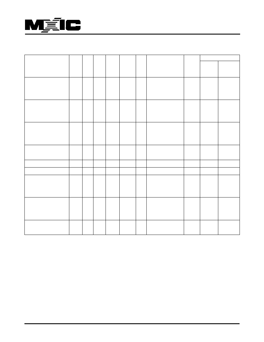
Table 2. AUTOSELECT CODES (High Voltage Method)
A22 A14
A8
A5
A3
Q8 to Q15
Description
CE# OE# WE#
to
to
A9
to
A6
to
to
A1 A0
Word
Byte
Q7 to Q0
A15 A10
A7
A4
A2
Mode
Mode
Manufacturer ID
L
L
H
X
X
VID
X
L
X
L
L
L
00
X
C2h
Cycle 1
L
L
H
22
X
7Eh
Cycle 2
L
L
H
X
X
VID
X
L
X
H
H
L
22
X
11h
Cycle 3
H
H
H
22
X
00h (bottom boot)
01h (top boot)
Sector Group
01h (protected),
Protection
L
L
H
SA
X
VID
X
L
X
L
H
L
X
X
Verification
00h (unprotected)
Secured Silicon
98h
Sector Indicator
(factory locked),
Bit (Q7), WP#
L
L
H
X
X
VID
X
L
X
L
H
H
X
X
protects top two
18h
address sector
(not factory locked)
Secured Silicon
88h
Sector Indicator
(factory locked),
Bit (Q7), WP# pro-
L
L
H
X
X
VID
X
L
X
L
H
H
X
X
tects bottom two
08h
address sector
(not factory locked)
Legend: L = Logic Low = VIL, H = Logic High = VIH, SA = Sector Address, X = Don't care.
29LA128MT/B

21
P/N:PM1170
REV. 0.04, JUL. 11, 2005
MX29LA128M T/B
REQUIREMENTS FOR READING ARRAY
DATA
To read array data from the outputs, the system must
drive the CE# and OE# pins to VIL. CE# is the power
control and selects the device. OE# is the output control
and gates array data to the output pins. WE# should re-
main at VIH.
The internal state machine is set for reading array data
upon device power-up, or after a hardware reset. This
ensures that no spurious alteration of the memory con-
tent occurs during the power transition. No command is
necessary in this mode to obtain array data. Standard
microprocessor read cycles that assert valid address on
the device address inputs produce valid data on the de-
vice data outputs. The device remains enabled for read
access until the command register contents are altered.
PAGE MODE READ
The MX29LA128M T/B offers "fast page mode read" func-
tion. This mode provides faster read access speed for
random locations within a page. The page size of the
device is 4 words/8 bytes. The appropriate page is se-
lected by the higher address bits A0~A1(Word Mode)/A-
1~A1(Byte Mode) This is an asynchronous operation; the
microprocessor supplies the specific word location.
The system performance could be enhanced by initiating
1 normal read and 3 fast page read (for word mode A0-
A1) or 7 fast page read (for byte mode A-1~A1). When
CE# is deasserted and reasserted for a subsequent ac-
cess, the access time is tACC or tCE. Fast page mode
accesses are obtained by keeping the "read-page ad-
dresses" constant and changing the "intra-read page"
addresses.
WRITING COMMANDS/COMMAND SE-
QUENCES
To program data to the device or erase sectors of memory,
the system must drive WE# and CE# to VIL, and OE# to
VIH.
An erase operation can erase one sector, multiple sec-
tors, or the entire device. Table indicates the address
space that each sector occupies. A "sector address"
consists of the address bits required to uniquely select a
sector. The Writing specific address and data commands
or sequences into the command register initiates device
operations. Table 1 defines the valid register command
sequences. Writing incorrect address and data values or
writing them in the improper sequence resets the device
to reading array data. Section has details on erasing a
sector or the entire chip, or suspending/resuming the erase
operation.
After the system writes the Automatic Select command
sequence, the device enters the Automatic Select mode.
The system can then read Automatic Select codes from
the internal register (which is separate from the memory
array) on Q7-Q0. Standard read cycle timings apply in
this mode. Refer to the Automatic Select Mode and Au-
tomatic Select Command Sequence section for more
information.
ICC2 in the DC Characteristics table represents the ac-
tive current specification for the write mode. The "AC
Characteristics" section contains timing specification
table and timing diagrams for write operations.
WRITE BUFFER
Write Buffer Programming allows the system to write a
maximum of 16 words/32 bytes in one programming op-
eration. This results in faster effective programming time
than the standard programming algorithms. See "Write
Buffer" for more information.
ACCELERATED PROGRAM OPERATION
The device offers accelerated program operations through
the ACC function. This is one of two functions provided
by the ACC pin. This function is primarily intended to
allow faster manufacturing throughput at the factory.
If the system asserts VHH on this pin, the device auto-
matically enters the aforementioned Unlock Bypass
mode, temporarily unprotects any protected sectors, and
uses the higher voltage on the pin to reduce the time
required for program operations. Removing VHH from the
ACC
pin must not be at VHH for operations other than accel-
erated programming, or device damage may result.

22
P/N:PM1170
REV. 0.04, JUL. 11, 2005
MX29LA128M T/B
STANDBY MODE
When using both pins of CE# and RESET#, the device
enter CMOS Standby with both pins held at VCC
±
0.3V.
If CE# and RESET# are held at VIH, but not within the
range of VCC
±
0.3V, the device will still be in the standby
mode, but the standby current will be larger. During Auto
Algorithm operation, VCC active current (ICC2) is required
even CE# = "H" until the operation is completed. The
device can be read with standard access time (tCE) from
either of these standby modes, before it is ready to read
data.
AUTOMATIC SLEEP MODE
The automatic sleep mode minimizes Flash device en-
ergy consumption. The device automatically enables this
mode when address remain stable for tACC+30ns. The
automatic sleep mode is independent of the CE#, WE#,
and OE# control signals. Standard address access tim-
ings provide new data when addresses are changed. While
in sleep mode, output data is latched and always avail-
able to the system. ICC4 in the DC Characteristics table
represents the automatic sleep mode current specifica-
tion.
OUTPUT DISABLE
With the OE# input at a logic high level (VIH), output
from the devices are disabled. This will cause the output
pins to be in a high impedance state.
RESET# OPERATION
The RESET# pin provides a hardware method of resetting
the device to reading array data. When the RESET# pin
is driven low for at least a period of tRP, the device
immediately terminates any operation in progress,
tristates all output pins, and ignores all read/write
commands for the duration of the RESET# pulse. The
device also resets the internal state machine to reading
array data. The operation that was interrupted should be
reinitiated once the device is ready to accept another
command sequence, to ensure data integrity
Current is reduced for the duration of the RESET# pulse.
When RESET# is held at VSS
±
0.3V, the device draws
CMOS standby current (ICC4). If RESET# is held at VIL
but not within VSS
±
0.3V, the standby current will be
greater.
The RESET# pin may be tied to system reset circuitry.
A system reset would that also reset the Flash memory,
enabling the system to read the boot-up firmware from
the Flash memory.
If RESET# is asserted during a program or erase
operation, the RY/BY# pin remains a "0" (busy) until the
internal reset operation is complete, which requires a time
of tREADY (during Embedded Algorithms). The system
can thus monitor RY/BY# to determine whether the reset
operation is complete. If RESET# is asserted when a
program or erase operation is completed within a time of
tREADY (not during Embedded Algorithms). The system
can read data tRH after the RESET# pin returns to VIH.
Refer to the AC Characteristics tables for RESET#
parameters and to Figure 3 for the timing diagram.
SECTOR GROUP PROTECT OPERATION
The MX29LA128M T/B features hardware sector group
protection. This feature will disable both program and
erase operations for these sector group protected. In
this device, a sector group consists of four adjacent sec-
tors which are protected or unprotected at the same time.
To activate this mode, the programming equipment must
force VID on address pin A9 and control pin OE#, (sug-
gest VID = 12V) A6 = VIL and CE# = VIL. (see Table 2)
Programming of the protection circuitry begins on the
falling edge of the WE# pulse and is terminated on the
rising edge. Please refer to sector group protect algo-
rithm and waveform.
MX29LA128M T/B also provides another method. Which
requires VID on the RESET# only. This method can be
implemented either in-system or via programming equip-
ment. This method uses standard microprocessor bus
cycle timing.
To verify programming of the protection circuitry, the pro-
gramming equipment must force VID on address pin A9
( with CE# and OE# at VIL and WE# at VIH). When
A1=1, it will produce a logical "1" code at device output
Q0 for a protected sector. Otherwise the device will pro-
duce 00H for the unprotected sector. In this mode, the
addresses, except for A1, are don't care. Address loca-
tions with A1 = VIL are reserved to read manufacturer
and device codes. (Read Silicon ID)

23
P/N:PM1170
REV. 0.04, JUL. 11, 2005
MX29LA128M T/B
It is also possible to determine if the group is protected
in the system by writing a Read Silicon ID command.
Performing a read operation with A1=VIH, it will produce
a logical "1" at Q0 for the protected sector.
CHIP UNPROTECT OPERATION
The MX29LA128M T/B also features the chip unprotect
mode, so that all sectors are unprotected after chip
unprotect is completed to incorporate any changes in
the code. It is recommended to protect all sectors before
activating chip unprotect mode.
To activate this mode, the programming equipment must
force VID on control pin OE# and address pin A9. The
CE# pins must be set at VIL. Pins A6 must be set to
VIH. (see Table 2) Refer to chip unprotect algorithm and
waveform for the chip unprotect algorithm. The unprotect
mechanism begins on the falling edge of the WE# pulse
and is terminated on the rising edge.
MX29LA128M T/B also provides another method. Which
requires VID on the RESET# only. This method can be
implemented either in-system or via programming equip-
ment. This method uses standard microprocessor bus
cycle timing.
It is also possible to determine if the chip is unprotect in
the system by writing the Read Silicon ID command.
Performing a read operation with A1=VIH, it will produce
00H at data outputs (Q0-Q7) for an unprotect sector. It is
noted that all sectors are unprotected after the chip
unprotect algorithm is completed.
WRITE PROTECT (WP#)
The write protect function provides a hardware method
to protect all sectors without using V
ID
.
If the system asserts VIL on the WP# pin, the device
disables program and erase functions in all sectors inde-
pendently of whether those sectors were protected or
unprotect using the method described in Sector/Sector
Group Protection and Chip Unprotect".
If the system asserts VIH on the WP# pin, the device
reverts to whether the sectors were last set to be pro-
tected or unprotect. That is, sector protection or
unprotection for the sectors depends on whether they were
last protected or unprotect using the method described in
"Sector/Sector Group Protection and Chip Unprotect".
Note that the WP# pin must not be left floating or uncon-
nected; inconsistent behavior of the device may result.
TEMPORARY SECTOR GROUP UNPROTECT
OPERATION
This feature allows temporary unprotect of previously
protected sector to change data in-system. The Tempo-
rary Sector Unprotect mode is activated by setting the
RESET# pin to VID(11.5V-12.5V). During this mode, for-
merly protected sectors can be programmed or erased
as unprotect sector. Once VID is remove from the RE-
SET# pin, all the previously protected sectors are pro-
tected again.
SILICON ID READ OPERATION
Flash memories are intended for use in applications where
the local CPU alters memory contents. As such, manu-
facturer and device codes must be accessible while the
device resides in the target system. PROM program-
mers typically access signature codes by raising A9 to
a high voltage. However, multiplexing high voltage onto
address lines is not generally desired system design prac-
tice.
MX29LA128M T/B provides hardware method to access
the silicon ID read operation. Which method requires VID
on A9 pin, VIL on CE#, OE#, A6, and A1 pins. Which
apply VIL on A0 pin, the device will output MXIC's manu-
facture code of which apply VIH on A0 pin, the device will
output MX29LA128M T/B device code.
VERIFY SECTOR GROUP PROTECT STATUS
OPERATION
MX29LA128M T/B provides hardware method for sector
group protect status verify. Which method requires VID
on A9 pin, VIH on WE# and A1 pins, VIL on CE#, OE#,
A6, and A0 pins, and sector address on A16 to A21 pins.
Which the identified sector is protected, the device will
output 01H. Which the identified sector is not protect, the
device will output 00H.
24
P/N:PM1170
REV. 0.04, JUL. 11, 2005
MX29LA128M T/B
DATA PROTECTION
The MX29LA128M T/B is designed to offer protection
against accidental erasure or programming caused by
spurious system level signals that may exist during power
transition. During power up the device automatically re-
sets the state machine in the Read mode. In addition,
with its control register architecture, alteration of the
memory contents only occurs after successful comple-
tion of specific command sequences. The device also
incorporates several features to prevent inadvertent write
cycles resulting from VCC power-up and power-down tran-
sition or system noise.
SECURED SILICON SECTOR
The MX29LA128M T/B features a OTP memory region
where the system may access through a command se-
quence to create a permanent part identification as so
called Electronic Serial Number (ESN) in the device.
Once this region is programmed, any further modifica-
tion on the region is impossible. The secured silicon sec-
tor is a 128 words in length, and uses a Secured Silicon
Sector Indicator Bit (Q7) to indicate whether or not the
Secured Silicon Sector is locked when shipped from the
factory. This bit is permanently set at the factory and
cannot be changed, which prevent duplication of a fac-
tory locked part. This ensures the security of the ESN
once the product is shipped to the field.
The MX29LA128M T/B offers the device with Secured
Silicon Sector either factory locked or customer lock-
able. The factory-locked version is always protected when
shipped from the factory , and has the Secured Silicon
Sector Indicator Bit permanently set to a "1". The cus-
tomer-lockable version is shipped with the Secured Sili-
con Sector unprotected, allowing customers to utilize that
sector in any form they prefer. The customer-lockable
version has the secured sector Indicator Bit permanently
set to a "0". Therefore, the Secured Silicon Sector Indi-
cator Bit prevents customer, lockable device from being
used to replace devices that are factory locked.
The system access the Secured Silicon Sector through
a command sequence (refer to "Enter Secured Silicon/
Exit Secured Silicon Sector command Sequence). After
the system has written the Enter Secured Silicon Sector
command sequence, it may read the Secured Silicon
Sector by using the address normally occupied by the
first sector SA0. Once entry the Secured Silicon Sector
the operation of boot sectors is disabled but the operation
of main sectors is as normally. This mode of operation
continues until the system issues the Exit Secured Sili-
con Sector command sequence, or until power is removed
from the device. On power-up, or following a hardware
reset, the device reverts to sending command to sector
SA0.
Secured Silicon
ESN factory
Customer
Sector address
locked
lockable
range
000000h-000007h
ESN
Determined by
000008h-00007Fh
Unavailable
Customer
FACTORY LOCKED:Secured Silicon Sector
Programmed and Protected At the Factory
In device with an ESN, the Secured Silicon Sector is
protected when the device is shipped from the factory.
The Secured Silicon Sector cannot be modified in any
way. A factory locked device has an 8-word random ESN
at address 000000h-000007h.
CUSTOMER LOCKABLE:Secured Silicon
Sector NOT Programmed or Protected At the
Factory
As an alternative to the factory-locked version, the device
may be ordered such that the customer may program
and protect the 128-word Secured Silicon Sector.
Programming and protecting the Secured Silicon Sector
must be used with caution since, once protected, there
is no procedure available for unprotected the Secured
Silicon Sector area and none of the bits in the Secured
Silicon Sector memory space can be modified in any
way.
The Secured Silicon Sector area can be protected using
one of the following procedures:
Write the three-cycle Enter Secured Silicon Sector Region
command sequence, and then follow the in-system
sector protect algorithm as shown in Figure 15, except
that RESET# may be at either VIH or VID. This allows in-
system protection of the Secured Silicon Sector without
raising any device pin to a high voltage. Note that method
is only applicable to the Secured Silicon Sector.

25
P/N:PM1170
REV. 0.04, JUL. 11, 2005
MX29LA128M T/B
Write the three-cycle Enter Secured Silicon Sector Region
command sequence, and then alternate method of sector
protection described in the :Sector Group Protection and
Unprotect" section.
Once the Secured Silicon Sector is programmed, locked
and verified, the system must write the Exit Secured
Silicon Sector Region command sequence to return to
reading and writing the remainder of the array.
LOW VCC WRITE INHIBIT
When VCC is less than VLKO the device does not ac-
cept any write cycles. This protects data during VCC
power-up and power-down. The command register and
all internal program/erase circuits are disabled, and the
device resets. Subsequent writes are ignored until VCC
is greater than VLKO. The system must provide the proper
signals to the control pins to prevent unintentional write
when VCC is greater than VLKO.
WRITE PULSE "GLITCH" PROTECTION
Noise pulses of less than 5ns (typical) on CE# or WE#
will not initiate a write cycle.
LOGICAL INHIBIT
Writing is inhibited by holding any one of OE# = VIL,
CE# = VIH or WE# = VIH. To initiate a write cycle CE#
and WE# must be a logical zero while OE# is a logical
one.
POWER-UP SEQUENCE
The MX29LA128M T/B powers up in the Read only mode.
In addition, the memory contents may only be altered
after successful completion of the predefined command
sequences.
POWER-UP WRITE INHIBIT
If WE#=CE#=VIL and OE#=VIH during power up, the
device does not accept commands on the rising edge of
WE#. The internal state machine is automatically reset
to the read mode on power-up.
POWER SUPPLY DE COUPLING
In order to reduce power switching effect, each device
should have a 0.1uF ceramic capacitor connected be-
tween its VCC and GND.
26
P/N:PM1170
REV. 0.04, JUL. 11, 2005
MX29LA128M T/B
TABLE 3. MX29LA128M T/B COMMAND DEFINITIONS
First Bus
Second Bus Third Bus
Fourth Bus
Fifth Bus
Sixth Bus
Command
Bus
Cycle
Cycle
Cycle
Cycle
Cycle
Cycle
Cycles Addr
Data
Addr
Data Addr Data Addr
Data
Addr Data Addr Data
Read (Note 5)
1
RA
RD
Reset (Note 6)
1
XXX
F0
Automatic Select (Note 7)
Manufacturer ID
Word
4
555
AA
2AA
55
555
90
X00
C2H
Byte
4
AAA
AA
555
55
AAA 90
X00
C2H
Device ID
Word
4
555
AA
2AA
55
555
90
X01
ID1
X0E ID2
X0F ID3
(Note 8)
Byte
4
AAA
AA
555
55
AAA 90
X02
ID1
X1C ID2
X1E ID3
Secured Sector Fact-
Word
4
555
AA
2AA
55
555
90
X03
see
ory Protect (Note 9)
Byte
4
AAA
AA
555
55
AAA 90
X06
note 9
Sector Group Protect
Word
4
555
AA
2AA
55
555
90
(SA)X02 XX00/
Verify (Note 10)
Byte
4
AAA
AA
555
55
AAA 90
(SA)X04 XX01
Enter Secured Silicon
Word
3
555
AA
2AA
55
555
88
Sector
Byte
3
AAA
AA
555
55
AAA 88
Exit Secured Silicon
Word
4
555
AA
2AA
55
555
90
XXX
00
Sector
Byte
4
AAA
AA
555
55
AAA 90
XXX
00
Program
Word
4
555
AA
2AA
55
555
A0
PA
PD
Byte
4
AAA
AA
555
55
AAA A0
PA
PD
Write to Buffer (Note 11)
Word
6
555
AA
2AA
55
SA
25
SA
WC
PA
PD
WBL PD
Byte
6
AAA
AA
555
55
SA
25
SA
BC
PA
PD
WBL PD
Program Buffer to Flash
Word
1
SA
29
Byte
1
SA
29
Write to Buffer Abort
Word
3
555
AA
2AA
55
555
F0
Reset (Note 12)
Byte
3
AAA
AA
555
55
AAA F0
Chip Erase
Word
6
555
AA
2AA
55
555
80
555
AA
2AA 55
555 10
Byte
6
AAA
AA
555
55
AAA 80
AAA
AA
555 55
AAA 10
Sector Erase
Word
6
555
AA
2AA
55
555
80
555
AA
2AA 55
SA
30
Byte
6
AAA
AA
555
55
AAA 80
AAA
AA
555 55
SA
30
Program/Erase Suspend (Note 13)
1
XXX
B0
Program/Erase Resume (Note 14)
1
XXX
30
CFI Query (Note 15)
Word
1
55
98
Byte
1
AA
98
SOFTWARE COMMAND DEFINITIONS
Device operations are selected by writing specific ad-
dress and data sequences into the command register.
Writing incorrect address and data values or writing them
in the improper sequence will reset the device to the
read mode. Table 3 defines the valid register command
sequences. Note that the Erase Suspend (B0H) and
Erase Resume (30H) commands are valid only while the
Sector Erase operation is in progress. Either of the two
reset command sequences will reset the device (when
applicable).
All addresses are latched on the falling edge of WE# or
CE#, whichever happens later. All data are latched on
rising edge of WE# or CE#, whichever happens first.

27
P/N:PM1170
REV. 0.04, JUL. 11, 2005
MX29LA128M T/B
Notes:
1. See Table 1 for descriptions of bus operations.
2. All values are in hexadecimal.
3. Except when reading array or automatic select data, all bus cycles are write operation.
4. Address bits are don't care for unlock and command cycles, except when PA or SA is required.
5. No unlock or command cycles required when device is in read mode.
6. The Reset command is required to return to the read mode when the device is in the automatic select mode or if
Q5 goes high.
7. The fourth cycle of the automatic select command sequence is a read cycle.
8. The device ID must be read in three cycles. The data is 01h for top boot and 00h for bottom boot.
9.
If WP# protects the top two address sectors, the data is 98h for factory locked and 18h for not factory locked. If
WP# protects the bottom two address sectors, the data is 88h for factory locked and 08h for not factor locked.
10. The data is 00h for an unprotected sector/sector block and 01h for a protected sector/sector block.
11. The total number of cycles in the command sequence is determined by the number of words written to the write
buffer. The maximum number of cycles in the command sequence is 21(Word Mode) / 37(Byte Mode).
12. Command sequence resets device for next command after aborted write-to-buffer operation.
13. The system may read and program functions in non-erasing sectors, or enter the automatic select mode, when in
the erase Suspend mode. The Erase Suspend command is valid only during a sector erase operation.
14. The Erase Resume command is valid only during the Erase Suspend mode.
15. Command is valid when device is ready to read array data or when device is in automatic select mode.
Legend:
X=Don't care
RA=Address of the memory location to be read.
RD=Data read from location RA during read operation.
PA=Address of the memory location to be programmed.
Addresses are latched on the falling edge of the WE# or
CE# pulse, whichever happen later.
DDI=Data of device identifier
C2H for manufacture code
PD=Data to be programmed at location PA. Data is
latched on the rising edge of WE# or CE# pulse.
SA=Address of the sector to be erase or verified (in
autoselect mode).
Address bits A21-A12 uniquely select any sector.
WBL=Write Buffer Location. Address must be within the
same write buffer page as PA.
WC=Word Count. Number of write buffer locations to load
minus 1.
BC=Byte Count. Number of write buffer locations to load
minus 1.

28
P/N:PM1170
REV. 0.04, JUL. 11, 2005
MX29LA128M T/B
READING ARRAY DATA
The device is automatically set to reading array data
after device power-up. No commands are required to re-
trieve data. The device is also ready to read array data
after completing an Automatic Program or Automatic
Erase algorithm.
After the device accepts an Erase Suspend command,
the device enters the Erase Suspend mode. The sys-
tem can read array data using the standard read tim-
ings, except that if it reads at an address within erase-
suspended sectors, the device outputs status data. Af-
ter completing a programming operation in the Erase
Suspend mode, the system may once again read array
data with the same exception. See Erase Suspend/Erase
Resume Commands for more information on this mode.
The system must issue the reset command to re-en-
able the device for reading array data if Q5 goes high, or
while in the automatic select mode. See the "Reset Com-
mand" section, next.
RESET COMMAND
Writing the reset command to the device resets the de-
vice to reading array data. Address bits are don't care for
this command.
The reset command may be written between the se-
quence cycles in an erase command sequence before
erasing begins. This resets the device to reading array
data. Once erasure begins, however, the device ignores
reset commands until the operation is complete.
The reset command may be written between the se-
quence cycles in a program command sequence before
programming begins. This resets the device to reading
array data (also applies to programming in Erase Sus-
pend mode). Once programming begins, however, the
device ignores reset commands until the operation is
complete.
The reset command may be written between the se-
quence cycles in an SILICON ID READ command se-
quence. Once in the SILICON ID READ mode, the reset
command must be written to return to reading array data
(also applies to SILICON ID READ during Erase Sus-
pend).
If Q5 goes high during a program or erase operation,
writing the reset command returns the device to reading
array data (also applies during Erase Suspend).
SILICON ID READ COMMAND SEQUENCE
The SILICON ID READ command sequence allows the
host system to access the manufacturer and devices
codes, and determine whether or not a sector is pro-
tected. Table 2 shows the address and data requirements.
This method is an alternative to that shown in Table 1,
which is intended for PROM programmers and requires
VID on address bit A9.
The SILICON ID READ command sequence is initiated
by writing two unlock cycles, followed by the SILICON
ID READ command. The device then enters the SILI-
CON ID READ mode, and the system may read at any
address any number of times, without initiating another
command sequence. A read cycle at address XX00h
retrieves the manufacturer code. A read cycle at address
XX01h returns the device code. A read cycle containing
a sector address (SA) and the address 02h returns 01h if
that sector is protected, or 00h if it is unprotected. Refer
to Table for valid sector addresses.
The system must write the reset command to exit the
automatic select mode and return to reading array data.
BYTE/WORD PROGRAM COMMAND SE-
QUENCE
The command sequence requires four bus cycles, and
is initiated by writing two unlock write cycles, followed
by the program set-up command. The program address
and data are written next, which in turn initiate the Em-
bedded Program algorithm. The system is not required
to provide further controls or timings. The device auto-
matically generates the program pulses and verifies the
programmed cell margin. Table 3 shows the address and
data requirements for the byte program command se-
quence.
When the Embedded Program algorithm is complete, the
device then returns to reading array data and addresses
are no longer latched. The system can determine the
status of the program operation by using Q7, Q6, or RY/
BY#. See "Write Operation Status" for information on
these status bits.
Any commands written to the device during the Embed-
ded Program Algorithm are ignored. Note that a hard-

29
P/N:PM1170
REV. 0.04, JUL. 11, 2005
MX29LA128M T/B
ware reset immediately terminates the programming op-
eration. The Byte/Word Program command sequence
should be reinitiated once the device has reset to read-
ing array data, to ensure data integrity.
Programming is allowed in any sequence and across
sector boundaries. A bit cannot be programmed from a
"0" back to a "1". Attempting to do so may halt the op-
eration and set Q5 to "1", or cause the Data# Polling
algorithm to indicate the operation was successful. How-
ever, a succeeding read will show that the data is still
"0". Only erase operations can convert a "0" to a "1".
Write Buffer Programming
Write Buffer Programming allows the system write to a
maximum of 16 words/32 bytes in one programming op-
eration. This results in faster effective programming time
than the standard programming algorithms. The Write
Buffer Programming command sequence is initiated by
first writing two unlock cycles. This is followed by a third
write cycle containing the Write Buffer Load command
written at the Sector Address in which programming will
occur. The fourth cycle writes the sector address and
the number of word locations, minus one, to be pro-
grammed. For example, if the system will program 6
unique address locations, then 05h should be written to
the device. This tells the device how many write buffer
addresses will be loaded with data and therefore when to
expect the Program Buffer to Flash command. The num-
ber of locations to program cannot exceed the size of
the write buffer or the operation will abort.
The fifth cycle writes the first address location and data
to be programmed. The write-buffer-page is selected by
address bits A
MAX
-4. All subsequent address/data pairs
must fall within the selected-write-buffer-page. The sys-
tem then writes the remaining address/data pairs into
the write buffer. Write buffer locations may be loaded in
any order.
The write-buffer-page address must be the same for all
address/data pairs loaded into the write buffer. (This
means Write Buffer Programming cannot be performed
across multiple write-buffer pages. This also means that
Write Buffer Programming cannot be performed across
multiple sectors. If the system attempts to load program-
ming data outside of the selected write-buffer page, the
operation will abort.
Note that if a Write Buffer address location is loaded
multiple times, the address/data pair counter will be
decremented for every data load operation. The host sys-
tem must therefore account for loading a write-buffer lo-
cation more than once. The counter decrements for each
data load operation, not for each unique write-buffer-ad-
dress location. Note also that if an address location is
loaded more than once into the buffer, the final data loaded
for that address will be programmed.
Once the specified number of write buffer locations have
been loaded, the system must then write the Program
Buffer to Flash command at the sector address. Any
other address and data combination aborts the Write
Buffer Programming operation. The device then begins
programming. Data polling should be used while monitor-
ing the last address location loaded into the write buffer.
Q7, Q6, Q5, and Q1 should be monitored to determine
the device status during Write Buffer Programming.
The write-buffer programming operation can be suspended
using the standard program suspend/resume commands.
Upon successful completion of the Write Buffer Program-
ming operation, the device is ready to execute the next
command.
The Write Buffer Programming Sequence can be aborted
in the following ways:
∑
Load a value that is greater than the page buffer size
during the Number of Locations to Program step.
∑
Write to an address in a sector different than the one
specified during the Write-Buffer-Load command.
∑
Write an Address/Data pair to a different write-buffer-
page than the one selected by the Starting Address
during the write buffer data loading stage of the op-
eration.
∑
Write data other than the Confirm Command after the
specified number of data load cycles.
The abort condition is indicated by Q1 = 1, Q7 = DATA#
(for the last address location loaded), Q6 = toggle, and
Q5=0. A Write-to-Buffer-Abort Reset command sequence
must be written to reset the device for the next opera-
tion. Note that the full 3-cycle Write-to-Buffer-Abort Re-
set command sequence is required when using Write-
Buffer-Programming features in Unlock Bypass mode.
Program Suspend/Program Resume Command
Sequence
The Program Suspend command allows the system to
interrupt a programming operation or a Write to Buffer

30
P/N:PM1170
REV. 0.04, JUL. 11, 2005
MX29LA128M T/B
programming operation so that data can be read from any
non-suspended sector. When the Program Suspend com-
mand is written during a programming process, the de-
vice halts the program operation within 15us maximum
(5 us typical) and updates the status bits. Addresses are
not required when writing the Program Suspend com-
mand.
After the programming operation has been suspended,
the system can read array data from any non-suspended
sector. The Program Suspend command may also be
issued during a programming operation while an erase is
suspended. In this case, data may be read from any
addresses not in Erase Suspend or Program Suspend. If
a read is needed from the Secured Silicon Sector area
(One-time Program area), then user must use the proper
command sequences to enter and exit this region.
The system may also write the autoselect command
sequence when the device is in the Program Suspend
mode. The system can read as many autoselect codes
as required. When the device exits the autoselect mode,
the device reverts to the Program Suspend mode, and
is ready for another valid operation. See Autoselect Com-
mand Sequence for more information.
After the Program Resume command is written, the de-
vice reverts to programming. The system can determine
the status of the program operation using the Q7 or Q6
status bits, just as in the standard program operation.
See Write Operation Status for more information.
SETUP AUTOMATIC CHIP/SECTOR ERASE
Chip erase is a six-bus cycle operation. There are two
"unlock" write cycles. These are followed by writing the
"set-up" command 80H. Two more "unlock" write cycles
are then followed by the chip erase command 10H, or
the sector erase command 30H.
The MX29LA128M T/B contains a Silicon-ID-Read op-
eration to supplement traditional PROM programming
methodology. The operation is initiated by writing the read
silicon ID command sequence into the command regis-
ter. Following the command write, a read cycle with
A1=VIL,A0=VIL retrieves the manufacturer code. A read
cycle with A1=VIL, A0=VIH returns the device code.
AUTOMATIC CHIP/SECTOR ERASE COM-
MAND
The device does not require the system to preprogram
prior to erase. The Automatic Erase algorithm automati-
cally pre-program and verifies the entire memory for an
all zero data pattern prior to electrical erase. The system
is not required to provide any controls or timings during
these operations. Table 3 shows the address and data
requirements for the chip erase command sequence.
Any commands written to the chip during the Automatic
Erase algorithm are ignored. Note that a hardware reset
during the chip erase operation immediately terminates
the operation. The Chip Erase command sequence should
be reinitiated once the device has returned to reading
array data, to ensure data integrity.
The system can determine the status of the erase op-
eration by using Q7, Q6, Q2, or RY/BY#. See "Write Op-
eration Status" for information on these status bits. When
the Automatic Erase algorithm is complete, the device
returns to reading array data and addresses are no longer
latched.
Figure 10 illustrates the algorithm for the erase opera-
tion. See the Erase/Program Operations tables in "AC
Characteristics" for parameters, and to Figure 9 for tim-
ing diagrams.

31
P/N:PM1170
REV. 0.04, JUL. 11, 2005
MX29LA128M T/B
SECTOR ERASE COMMANDS
The Automatic Sector Erase does not require the device
to be entirely pre-programmed prior to executing the Au-
tomatic Set-up Sector Erase command and Automatic
Sector Erase command. Upon executing the Automatic
Sector Erase command, the device will automatically
program and verify the sector(s) memory for an all-zero
data pattern. The system is not required to provide any
control or timing during these operations.
When the sector(s) is automatically verified to contain
an all-zero pattern, a self-timed sector erase and verify
begin. The erase and verify operations are complete
when the data on Q7 is "1" and the data on Q6 stops
toggling for two consecutive read cycles, at which time
the device returns to the Read mode. The system is not
required to provide any control or timing during these
operations.
When using the Automatic Sector Erase algorithm, note
that the erase automatically terminates when adequate
erase margin has been achieved for the memory array
(no erase verification command is required). Sector erase
is a six-bus cycle operation. There are two "unlock" write
cycles. These are followed by writing the set-up com-
mand 80H. Two more "unlock" write cycles are then fol-
lowed by the sector erase command 30H. The sector
address is latched on the falling edge of WE# or CE#,
whichever happens later , while the command (data) is
latched on the rising edge of WE# or CE#, whichever
happens first. Sector addresses selected are loaded
into internal register on the sixth falling edge of WE# or
CE#, whichever happens later. Each successive sector
load cycle started by the falling edge of WE# or CE#,
whichever happens later must begin within 50us from
the rising edge of the preceding WE# or CE#, whichever
happens first. Otherwise, the loading period ends and
internal auto sector erase cycle starts. (Monitor Q3 to
determine if the sector erase timer window is still open,
see section Q3, Sector Erase Timer.) Any command other
than Sector Erase(30H) or Erase Suspend(B0H) during
the time-out period resets the device to read mode.
ERASE SUSPEND
This command only has meaning while the state ma-
chine is executing Automatic Sector Erase operation,
and therefore will only be responded during Automatic
Sector Erase operation. When the Erase Suspend com-
mand is issued during the sector erase operation, the
device requires a maximum 20us to suspend the sector
erase operation. However, When the Erase Suspend com-
mand is written during the sector erase time-out, the
device immediately terminates the time-out period and
suspends the erase operation. After this command has
been executed, the command register will initiate erase
suspend mode. The state machine will return to read
mode automatically after suspend is ready. At this time,
state machine only allows the command register to re-
spond to the Erase Resume, program data to, or read
data from any sector not selected for erasure.
The system can determine the status of the program
operation using the Q7 or Q6 status bits, just as in the
standard program operation. After an erase-suspend pro-
gram operation is complete, the system can once again
read array data within non-suspended blocks.
ERASE RESUME
This command will cause the command register to clear
the suspend state and return back to Sector Erase mode
but only if an Erase Suspend command was previously
issued. Erase Resume will not have any effect in all
other conditions. Another Erase Suspend command can
be written after the chip has resumed erasing.
32
P/N:PM1170
REV. 0.04, JUL. 11, 2005
MX29LA128M T/B
Table 4-1. CFI mode: Identification Data Values
(All values in these tables are in hexadecimal)
Description
Address h
Address h
Data h
(x16)
(x8)
Query-unique ASCII string "QRY"
10
20
0051
11
22
0052
12
24
0059
Primary vendor command set and control interface ID code
13
26
0002
14
28
0000
Address for primary algorithm extended query table
15
2A
0040
16
2C
0000
Alternate vendor command set and control interface ID code (none)
17
2E
0000
18
30
0000
Address for secondary algorithm extended query table (none)
19
32
0000
1A
34
0000
Table 4-2. CFI Mode: System Interface Data Values
Description
Address h
Address h
Data h
(x16)
(x8)
VCC supply, minimum (2.7V)
1B
36
0027
VCC supply, maximum (3.6V)
1C
38
0036
VPP supply, minimum (none)
1D
3A
0000
VPP supply, maximum (none)
1E
3C
0000
Typical timeout for single word/byte write (2
N
us)
1F
3E
0007
Typical timeout for maximum size buffer write (2
N
us)
20
40
0007
Typical timeout for individual block erase (2
N
ms)
21
42
000A
Typical timeout for full chip erase (2
N
ms)
22
44
0000
Maximum timeout for single word/byte write times (2
N
X Typ)
23
46
0001
Maximum timeout for maximum size buffer write times (2
N
X Typ)
24
48
0005
Maximum timeout for individual block erase times (2
N
X Typ)
25
4A
0004
Maximum timeout for full chip erase times (not supported)
26
4C
0000
QUERY COMMAND AND COMMON FLASH
INTERFACE (CFI) MODE
MX29LA128M T/B is capable of operating in the CFI mode.
This mode all the host system to determine the manu-
facturer of the device such as operating parameters and
configuration. Two commands are required in CFI mode.
Query command of CFI mode is placed first, then the
Reset command exits CFI mode. These are described in
Table 4.
The single cycle Query command is valid only when the
device is in the Read mode, including Erase Suspend,
Standby mode, and Read ID mode; however, it is ignored
otherwise.
The Reset command exits from the CFI mode to the
Read mode, or Erase Suspend mode, or read ID mode.
The command is valid only when the device is in the CFI
mode.

33
P/N:PM1170
REV. 0.04, JUL. 11, 2005
MX29LA128M T/B
Description
Address h
Address h
Data h
(x16)
(x8)
Device size (2
n
bytes)
27
4E
0018
Flash device interface code
28
50
0002
29
52
0000
Maximum number of bytes in multi-byte write =2
N
2A
54
0005
2B
56
0000
Number of erase block regions (X=# of Erase Block Regions)
2C
58
0002
Erase block region 1 information
2D
5A
0007
[2E,2D] = # of blocks in region -1
2E
5C
0000
[30, 2F] = size in multiples of 256-bytes
2F
5E
0020
30
60
0000
31
62
00FE
Erase Block Region 2 Information (refer to CFI publication 100)
32
64
0000
33
66
0000
34
68
0001
35
6A
0000
Erase Block Region 3 Information (refer to CFI publication 100)
36
6C
0000
37
6E
0000
38
70
0000
39
72
0000
Erase Block Region 4 Information (refer to CFI publication 100)
3A
74
0000
3B
76
0000
3C
78
0000
Table 4-3. CFI Mode: Device Geometry Data Values
34
P/N:PM1170
REV. 0.04, JUL. 11, 2005
MX29LA128M T/B
Description
Address h
Address h
Data h
(x16)
(x8)
Query-unique ASCII string "PRI"
40
80
0050
41
82
0052
42
84
0049
Major version number, ASCII
43
86
0031
Minor version number, ASCII
44
88
0033
Address sensitive unlock (0=required, 1= not required)
45
8A
0000
Erase suspend (2= to read and write)
46
8C
0002
Sector protect (N= # of sectors/group)
47
8E
0001
Temporary sector unprotect (1=supported)
48
90
0001
Sector protect/unprotect scheme
49
92
0004
Simultaneous R/W operation (0=not supported)
4A
94
0000
Burst mode type (0=not supported)
4B
96
0000
Page mode type (1=4 word page)
4C
98
0001
ACC (Acceleration) Supply Minimum
4D
9A
00B5
00h=Not Supported, D7-D4: Volt, D3-D0:100mV
ACC (Acceleration) Supply Maximum
4E
9C
00C5
00h=Not Supported, D7-D4: Volt, D3-D0:100mV
Top/Bottom Boot Sector Flag
4F
9E
0002/
02h=Bottom Boot Device, 03h=Top Boot Device
0003
04h=uniform sectors bottom WP# protect,
05h=uniform sectors top WP# protect
Program Suspend
50
A0
0001
00h=Not Supported, 01h=Supported
Table 4-4. CFI Mode: Primary Vendor-Specific Extended Query Data Values
35
P/N:PM1170
REV. 0.04, JUL. 11, 2005
MX29LA128M T/B
Table 5. Write Operation Status
WRITE OPERATION STATUS
The device provides several bits to determine the status
of a write operation: Q2, Q3, Q5, Q6, Q7, and RY/BY#.
Table 5 and the following subsections describe the func-
tions of these bits. Q7, RY/BY#, and Q6 each offer a
method for determining whether a program or erase op-
eration is complete or in progress. These three bits are
discussed first.
Status
Q7
Q6
Q5
Q3
Q2
Q1
RY/BY#
Byte/Word Program in Auto Program Algorithm
Q7#
Toggle
0
N/A
No
0
0
Toggle
Auto Erase Algorithm
0
Toggle
0
1
Toggle
N/A
0
Erase Suspend Read
1
No
0
N/A
Toggle
N/A
1
Erase
(Erase Suspended Sector)
Toggle
Suspended
Erase Suspend Read
Data
Data
Data
Data
Data
Data
1
Mode
(Non-Erase Suspended Sector)
Erase Suspend Program
Q7#
Toggle
0
N/A
N/A
N/A
0
Program-Suspended Read
Invalid (not allowed)
1
Program
(Program-Suspended Sector)
Suspend
Program-Suspended Read
Data
1
(Non-Program-Suspended Sector)
Write-to-Buffer
Busy
Q7#
Toggle
0
N/A
N/A
0
0
Abort
Q7#
Toggle
0
N/A
N/A
1
0
Notes:
1. Q5 switches to "1" when an Word/Byte Program, Erase, or Write-to-Buffer operation has exceeded the maximum
timing limits. Refer to the section on Q5 for more information.
2. Q7 and Q2 require a valid address when reading status information. Refer to the appropriate subsection for further
details.
3. The Data# Polling algorithm should be used to monitor the last loaded write-buffer address location.
4. Q1 switches to "1" when the device has aborted the write-to-buffer operation.

36
P/N:PM1170
REV. 0.04, JUL. 11, 2005
MX29LA128M T/B
Q7: Data# Polling
The Data# Polling bit, Q7, indicates to the host system
whether an Automatic Algorithm is in progress or com-
pleted, or whether the device is in Erase Suspend. Data#
Polling is valid after the rising edge of the final WE# pulse
in the program or erase command sequence.
During the Automatic Program algorithm, the device out-
puts on Q7 the complement of the datum programmed
to Q7. This Q7 status also applies to programming dur-
ing Erase Suspend. When the Automatic Program algo-
rithm is complete, the device outputs the datum pro-
grammed to Q7. The system must provide the program
address to read valid status information on Q7. If a pro-
gram address falls within a protected sector, Data# Poll-
ing on Q7 is active for approximately 1 us, then the de-
vice returns to reading array data.
During the Automatic Erase algorithm, Data# Polling pro-
duces a "0" on Q7. When the Automatic Erase algorithm
is complete, or if the device enters the Erase Suspend
mode, Data# Polling produces a "1" on Q7. This is analo-
gous to the complement/true datum output described for
the Automatic Program algorithm: the erase function
changes all the bits in a sector to "1" prior to this, the
device outputs the "complement," or "0". The system must
provide an address within any of the sectors selected for
erasure to read valid status information on Q7.
After an erase command sequence is written, if all sec-
tors selected for erasing are protected, Data# Polling on
Q7 is active for approximately 100 us, then the device
returns to reading array data. If not all selected sectors
are protected, the Automatic Erase algorithm erases the
unprotected sectors, and ignores the selected sectors
that are protected.
When the system detects Q7 has changed from the
complement to true data, it can read valid data at Q7-Q0
on the following read cycles. This is because Q7 may
change asynchronously with Q0-Q6 while Output Enable
(OE#) is asserted low.
Q6:Toggle BIT I
Toggle Bit I on Q6 indicates whether an Automatic Pro-
gram or Erase algorithm is in progress or complete, or
whether the device has entered the Erase Suspend mode.
Toggle Bit I may be read at any address, and is valid
after the rising edge of the final WE# or CE#, whichever
happens first pulse in the command sequence (prior to
the program or erase operation), and during the sector
time-out.
During an Automatic Program or Erase algorithm opera-
tion, successive read cycles to any address cause Q6
to toggle. The system may use either OE# or CE# to
control the read cycles. When the operation is complete,
Q6 stops toggling.
After an erase command sequence is written, if all sec-
tors selected for erasing are protected, Q6 toggles for
100us and returns to reading array data. If not all se-
lected sectors are protected, the Automatic Erase algo-
rithm erases the unprotected sectors, and ignores the
selected sectors that are protected.
The system can use Q6 and Q2 together to determine
whether a sector is actively erasing or is erase suspended.
When the device is actively erasing (that is, the Auto-
matic Erase algorithm is in progress), Q6 toggling. When
the device enters the Erase Suspend mode, Q6 stops
toggling. However, the system must also use Q2 to de-
termine which sectors are erasing or erase-suspended.
Alternatively, the system can use Q7.
If a program address falls within a protected sector, Q6
toggles for approximately 2us after the program com-
mand sequence is written, then returns to reading array
data.
Q6 also toggles during the erase-suspend-program mode,
and stops toggling once the Automatic Program algo-
rithm is complete.
Table 5 shows the outputs for Toggle Bit I on Q6.
Q2:Toggle Bit II
The "Toggle Bit II" on Q2, when used with Q6, indicates
whether a particular sector is actively erasing (that is,
the Automatic Erase algorithm is in process), or whether
that sector is erase-suspended. Toggle Bit II is valid
after the rising edge of the final WE# or CE#, whichever
happens first pulse in the command sequence.
Q2 toggles when the system reads at addresses within
those sectors that have been selected for erasure. (The
system may use either OE# or CE# to control the read
cycles.) But Q2 cannot distinguish whether the sector
is actively erasing or is erase-suspended. Q6, by com-

37
P/N:PM1170
REV. 0.04, JUL. 11, 2005
MX29LA128M T/B
parison, indicates whether the device is actively eras-
ing, or is in Erase Suspend, but cannot distinguish which
sectors are selected for erasure. Thus, both status bits
are required for sectors and mode information. Refer to
Table 5 to compare outputs for Q2 and Q6.
Reading Toggle Bits Q6/ Q2
Whenever the system initially begins reading toggle bit
status, it must read Q7-Q0 at least twice in a row to
determine whether a toggle bit is toggling. Typically, the
system would note and store the value of the toggle bit
after the first read. After the second read, the system
would compare the new value of the toggle bit with the
first. If the toggle bit is not toggling, the device has
completed the program or erase operation. The system
can read array data on Q7-Q0 on the following read cycle.
However, if after the initial two read cycles, the system
determines that the toggle bit is still toggling, the sys-
tem also should note whether the value of Q5 is high
(see the section on Q5). If it is, the system should then
determine again whether the toggle bit is toggling, since
the toggle bit may have stopped toggling just as Q5 went
high. If the toggle bit is no longer toggling, the device
has successfully completed the program or erase opera-
tion. If it is still toggling, the device did not complete the
operation successfully, and the system must write the
reset command to return to reading array data.
The remaining scenario is that system initially determines
that the toggle bit is toggling and Q5 has not gone high.
The system may continue to monitor the toggle bit and
Q5 through successive read cycles, determining the sta-
tus as described in the previous paragraph. Alternatively,
it may choose to perform other system tasks. In this
case, the system must start at the beginning of the al-
gorithm when it returns to determine the status of the
operation.
Q5:Program/Erase Timing
Q5 will indicate if the program or erase time has exceeded
the specified limits (internal pulse count). Under these
conditions Q5 will produce a "1". This time-out condition
indicates that the program or erase cycle was not suc-
cessfully completed. Data# Polling and Toggle Bit are
the only operating functions of the device under this con-
dition.
If this time-out condition occurs during sector erase op-
eration, it specifies that a particular sector is bad and it
may not be reused. However, other sectors are still func-
tional and may be used for the program or erase opera-
tion. The device must be reset to use other sectors.
Write the Reset command sequence to the device, and
then execute program or erase command sequence. This
allows the system to continue to use the other active
sectors in the device.
If this time-out condition occurs during the chip erase
operation, it specifies that the entire chip is bad or com-
bination of sectors are bad.
If this time-out condition occurs during the byte/word pro-
gramming operation, it specifies that the entire sector
containing that byte is bad and this sector may not be
reused, (other sectors are still functional and can be re-
used).
The time-out condition may also appear if a user tries to
program a non blank location without erasing. In this
case the device locks out and never completes the Au-
tomatic Algorithm operation. Hence, the system never
reads a valid data on Q7 bit and Q6 never stops toggling.
Once the Device has exceeded timing limits, the Q5 bit
will indicate a "1". Please note that this is not a device
failure condition since the device was incorrectly used.
The Q5 failure condition may appear if the system tries
to program a to a "1" location that is previously pro-
grammed to "0". Only an erase operation can change a
"0" back to a "1". Under this condition, the device halts
the operation, and when the operation has exceeded the
timing limits, Q5 produces a "1".
Q3:Sector Erase Timer
After the completion of the initial sector erase command
sequence, the sector erase time-out will begin. Q3 will
remain low until the time-out is complete. Data# Polling
and Toggle Bit are valid after the initial sector erase com-
mand sequence.
If Data# Polling or the Toggle Bit indicates the device
has been written with a valid erase command, Q3 may
be used to determine if the sector erase timer window is
still open. If Q3 is high ("1") the internally controlled
erase cycle has begun; attempts to write subsequent
commands to the device will be ignored until the erase
operation is completed as indicated by Data# Polling or

38
P/N:PM1170
REV. 0.04, JUL. 11, 2005
MX29LA128M T/B
Toggle Bit. If Q3 is low ("0"), the device will accept addi-
tional sector erase commands. To insure the command
has been accepted, the system software should check
the status of Q3 prior to and following each subsequent
sector erase command. If Q3 were high on the second
status check, the command may not have been accepted.
If the time between additional erase commands from the
system can be less than 50us, the system need not to
monitor Q3.
Q1: Write-to-Buffer Abort
Q1 indicates whether a Write-to-Buffer operation was
aborted. Under these conditions Q1 produces a "1". The
system must issue the Write-to-Buffer-Abort-Reset com-
mand sequence to return the device to reading array data.
See Write Buffer section for more details.
RY/BY#:READY/BUSY OUTPUT
The RY/BY# is a dedicated, open-drain output pin that
indicates whether an Embedded Algorithm is in progress
or complete. The RY/BY# status is valid after the rising
edge of the final WE# pulse in the command sequence.
Since RY/BY# is an open-drain output, several RY/BY#
pins can be tied together in parallel with a pull-up resistor
to VCC .
If the output is low (Busy), the device is actively erasing
or programming. (This includes programming in the Erase
Suspend mode.) If the output is high (Ready), the device
is ready to read array data (including during the Erase
Suspend mode), or is in the standby mode.

39
P/N:PM1170
REV. 0.04, JUL. 11, 2005
MX29LA128M T/B
ABSOLUTE MAXIMUM RATINGS
Storage Temperature
Plastic Packages . . . . . . . . . . . . . ..... -65
o
C to +150
o
C
Ambient Temperature
with Power Applied. . . . . . . . . . . . . .... -65
o
C to +125
o
C
Voltage with Respect to Ground
VCC (Note 1) . . . . . . . . . . . . . . . . . -0.5 V to +4.0 V
A9, OE#, and
RESET# (Note 2) . . . . . . . . . . . ....-0.5 V to +12.5 V
All other pins (Note 1) . . . . . . . -0.5 V to VCC +0.5 V
Output Short Circuit Current (Note 3) . . . . . . 200 mA
Notes:
1. Minimum DC voltage on input or I/O pins is -0.5 V.
During voltage transitions, input or I/O pins may over-
shoot VSS to -2.0 V for periods of up to 20 ns. Maxi-
mum DC voltage on input or I/O pins is VCC +0.5 V.
During voltage transitions, input or I/O pins may over-
shoot to VCC +2.0 V for periods up to 20ns.
2. Minimum DC input voltage on pins A9, OE#, and
RESET# is -0.5 V. During voltage transitions, A9, OE#,
and RESET# may overshoot VSS to -2.0 V for peri-
ods of up to 20 ns. Maximum DC input voltage on pin
A9 is +12.5 V which may overshoot to 14.0 V for peri-
ods up to 20 ns.
3. No more than one output may be shorted to ground at
a time. Duration of the short circuit should not be
greater than one second.
Stresses above those listed under "Absolute Maximum
Ratings" may cause permanent damage to the device.
This is a stress rating only; functional operation of the
device at these or any other conditions above those in-
dicated in the operational sections of this data sheet is
not implied. Exposure of the device to absolute maxi-
mum rating conditions for extended periods may affect
device reliability.
OPERATING RATINGS
Commercial (C) Devices
Ambient Temperature (T
A
). . . . . . . . . . . . 0
∞
C to +70
∞
C
Industrial (I) Devices
Ambient Temperature (T
A
). . . . . . . . . . -40
∞
C to +85
∞
C
VCC
Supply Voltages
VCC for full voltage range. . . . . . . . . . . +2.7 V to 3.6 V
Operating ranges define those limits between which the
functionality of the device is guaranteed.
40
P/N:PM1170
REV. 0.04, JUL. 11, 2005
MX29LA128M T/B
Notes:
1. On the WP#/ACC pin only, the maximum input load current when WP# = VIL is
±
5.0uA.
2. Maximum ICC specifications are tested with VCC = VCC max.
3. The ICC current listed is typically is less than 2 mA/MHz, with OE# at VIH. Typical specifications are for VCC =
3.0V.
4. ICC active while Embedded Erase or Embedded Program is in progress.
5. Automatic sleep mode enables the low power mode when addresses remain stable for t ACC + 30 ns.
6. Not 100% tested.
7. A9=12.5V when TA=0
∞
C to 85
∞
C, A9=12V when when TA=-40
∞
C to 0
∞
C.
DC CHARACTERISTICS
TA=-40
∞∞
∞∞
∞
C to 85
∞∞
∞∞
∞
C, VCC=2.7V~3.6V (VCC=3.0V~3.6V for 90R)
Para-
meter Description
Test Conditions
Min.
Typ.
Max.
Unit
I LI
Input Load Current (Note 1)
VIN = VSS to VCC ,
±
1.0
uA
VCC = VCC max
I LIT
A9 Input Leakage Current
VCC=VCC max; A9 = 12.5V
35
uA
I LO
Output Leakage Current
VOUT = VSS to VCC ,
±
1.0
uA
VCC = VCC max
ICC1
VCC Initial Read Current
CE# = VIL,
10 MHz
35
50
mA
(Notes 2,3)
OE# = VIH
5 MHz
18
25
mA
1 MHz
5
20
mA
ICC2
VCC Intra-Page Read
CE# = VIL ,
10 MHz
5
20
mA
Current (Notes 2,3)
OE# = VIH
40 MHz
10
40
mA
ICC3
VCC Active Write Current
CE# = VIL , OE# = VIH
50
60
mA
(Notes 2,4,6)
ICC4
VCC Standby Current
CE#, RESET# = VCC
±
0.3V
20
50
uA
(Note 2)
WP# = VIH
ICC5
VCC Reset Current
RESET# = VSS
±
0.3V
20
50
uA
(Note 2)
WP# = VIH
ICC6
Automatic Sleep Mode
VIL = VSS
±
0.3 V,
20
50
uA
(Notes 2,5)
VIH = VCC
±
0.3 V,
WP# = VIH
VIL
Input Low Voltage
-0.5
0.8
V
VIH
Input High Voltage
0.7xVCC
VCC+0.5
V
VHH
Voltage for ACC Program
VCC = 2.7V ~ 3.6V
11.5
12.0
12.5
V
Acceleration
VID
Voltage for Autoselect and
VCC = 3.0 V
±
10%
11.5
12.0
12.5
V
Temporary Sector Unprotect
VOL
Output Low Voltage
IOL= 4.0mA,VCC=VCC min
0.45
V
VOH1 Output High Voltage
IOH=-2.0mA,VCC=VCC min
0.85VCC
V
VOH2
IOH=-100uA,VCC=VCC min
VCC-0.4
V
VLKO Low VCC Lock-Out Voltage
2.3
2.5
V
(Note 4)
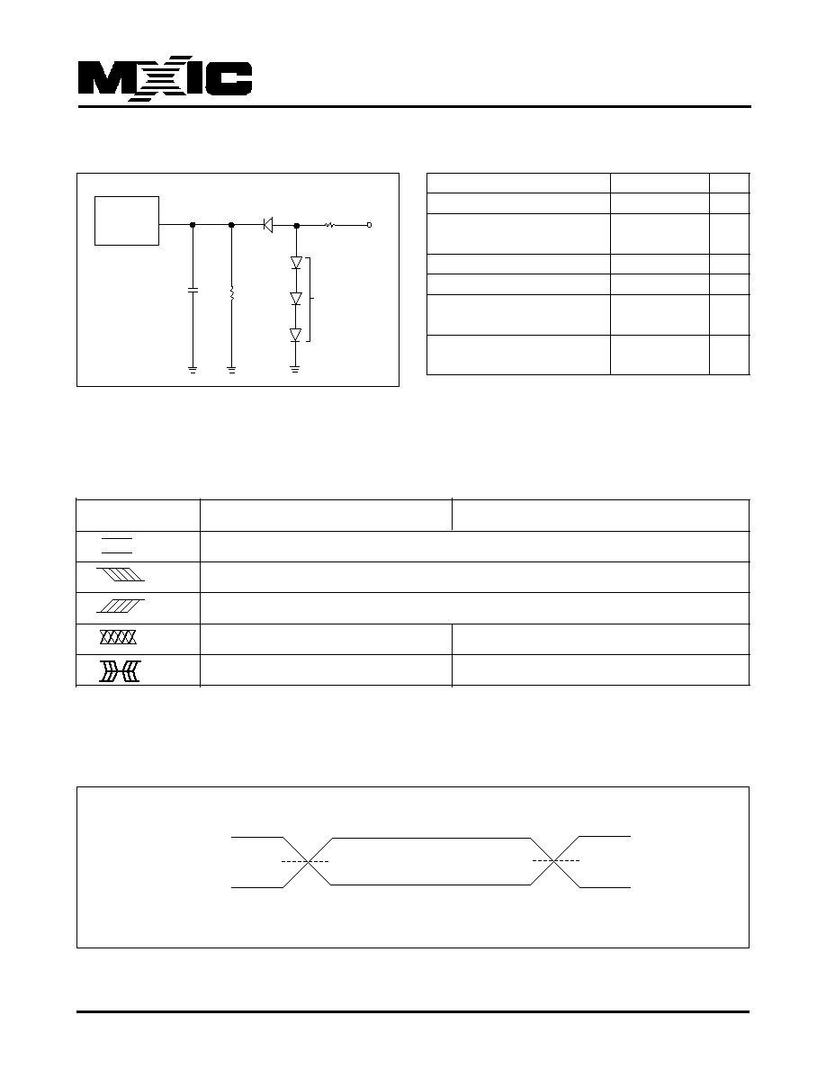
41
P/N:PM1170
REV. 0.04, JUL. 11, 2005
MX29LA128M T/B
SWITCHING TEST CIRCUITS
WAVEFORM
INPUTS
OUTPUTS
Steady
Changing from H to L
Changing from L to H
Don't Care, Any Change Permitted
Changing, State Unknown
Does Not Apply
Center Line is High Impedance State(High Z)
KEY TO SWITCHING WAVEFORMS
SWITCHING TEST WAVEFORMS
TEST SPECIFICATIONS
Test Condition
All Speeds
Unit
Output Load
1 TTL gate
Output Load Capacitance, CL
30
pF
(including jig capacitance)
Input Rise and Fall Times
5
ns
Input Pulse Levels
0.0-3.0
V
Input timing measurement
1.5
V
reference levels
Output timing measurement
1.5
V
reference levels
DEVICE UNDER
TEST
DIODES=IN3064
OR EQUIVALENT
CL
6.2K ohm
2.7K ohm
3.3V
1.5V
1.5V
Measurement Level
3.0V
0.0V
OUTPUT
INPUT
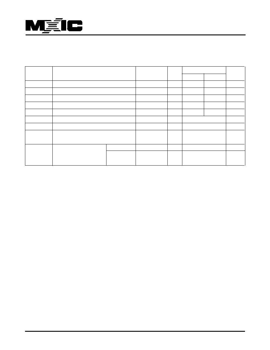
42
P/N:PM1170
REV. 0.04, JUL. 11, 2005
MX29LA128M T/B
AC CHARACTERISTICS
Read-Only Operations
TA=-40
∞∞
∞∞
∞
C to 85
∞∞
∞∞
∞
C, VCC=2.7V~3.6V
(VCC=3.0V~3.6V for 90R)
Parameter
Speed Options
Std.
Description
Test Setup
90R
100
Unit
tRC
Read Cycle Time (Note 1)
Min
90
100
ns
tACC
Address to Output Delay
CE#, OE#=VIL
Max
90
100
ns
tCE
Chip Enable to Output Delay
OE#=VIL
Max
90
100
ns
tPACC
Page Access Time
Max
25
25
ns
tOE
Output Enable to Output Delay
Max
35
35
ns
tDF
Chip Enable to Output High Z (Note 1)
Max
16
ns
tDF
Output Enable to Output High Z (Note 1)
Max
16
ns
tOH
Output Hold Time From Address, CE#
Min
0
ns
or OE#, whichever Occurs First
Read
Min
35
ns
tOEH
Output Enable Hold Time
Toggle and
Min
10
ns
(Note 1)
Data# Polling
Notes:
1. Not 100% tested.
2. See SWITCHING TEST CIRCUITS and TEST SPECIFICATIONS TABLE for test specifications.
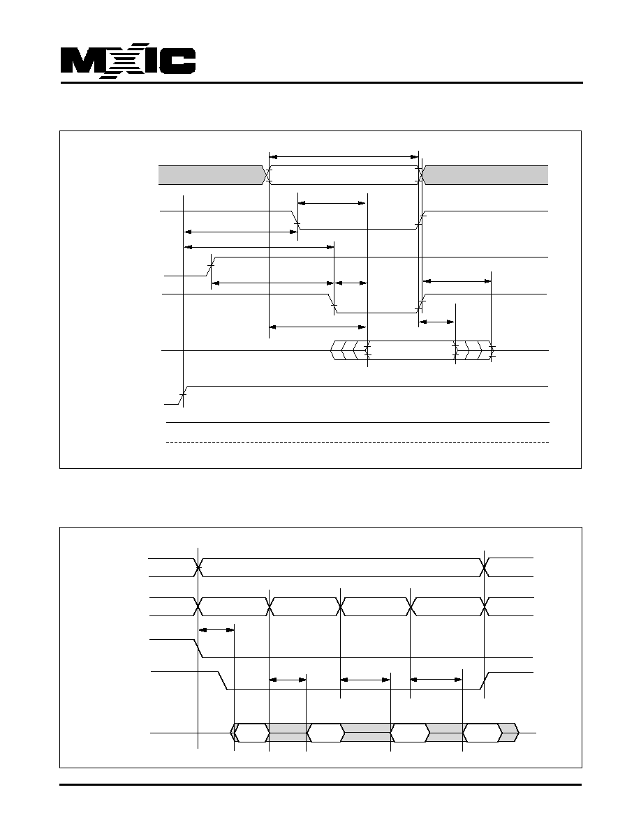
43
P/N:PM1170
REV. 0.04, JUL. 11, 2005
MX29LA128M T/B
Figure 1. READ TIMING WAVEFORMS
Addresses
CE#
OE#
tACC
WE#
VIH
VIL
VIH
VIL
VIH
VIL
VIH
VIL
0V
VIH
VIL
VOH
VOL
HIGH Z
HIGH Z
DATA Valid
tOE
tOEH
tDF
tCE
tRH
tRH
tRC
Outputs
RESET#
RY/BY#
tOH
ADD Valid
Figure 2. PAGE READ TIMING WAVEFORMS
Same Page
A2-A21
(A-1), A0~A2
CE#
OE#
Output
tACC
tPACC
tPACC
tPACC
Qa
Qb
Qc
Qd
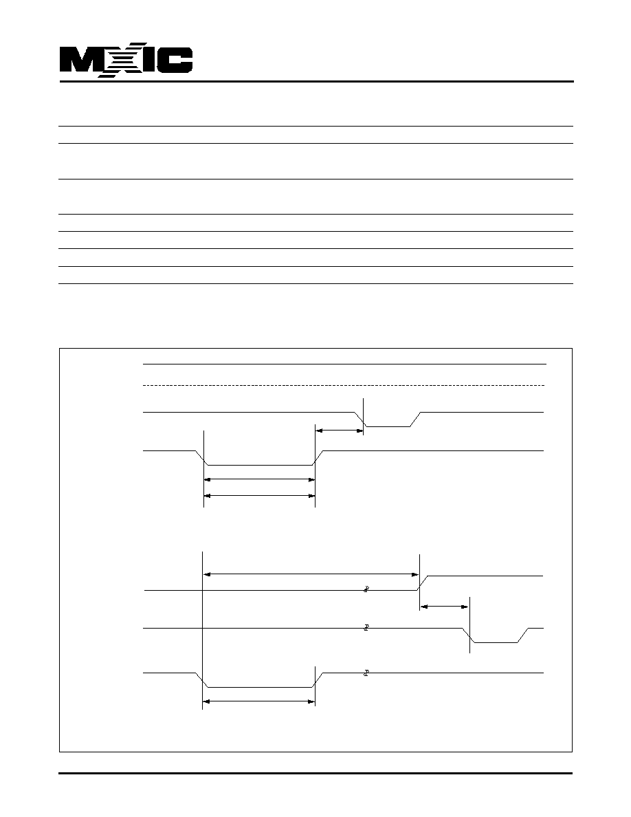
44
P/N:PM1170
REV. 0.04, JUL. 11, 2005
MX29LA128M T/B
Figure 3. RESET# TIMING WAVEFORM
AC CHARACTERISTICS
Parameter
Description
Test Setup
All Speed Options Unit
tREADY1
RESET# PIN Low (During Automatic Algorithms)
MAX
20
us
to Read or Write (See Note)
tREADY2
RESET# PIN Low (NOT During Automatic Algorithms)
MAX
500
ns
to Read or Write (See Note)
tRP
RESET# Pulse Width (NOT During Automatic Algorithms)
MIN
500
ns
tRH
RESET# High Time Before Read (See Note)
MIN
50
ns
tRB
RY/BY# Recovery Time(to CE#, OE# go low)
MIN
0
ns
tRPD
RESET# Low to Standby Mode
MIN
20
us
Note:Not 100% tested
tRH
tRB
tReady1
tRP
tRP
tReady2
RY/BY#
CE#, OE#
RESET#
Reset Timing NOT during Automatic Algorithms
Reset Timing during Automatic Algorithms
RY/BY#
CE#, OE#
RESET#
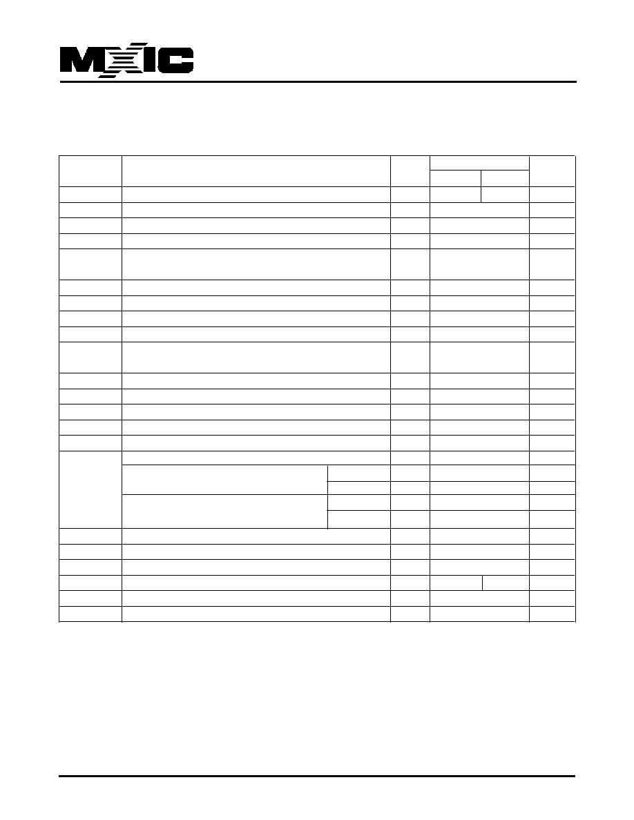
45
P/N:PM1170
REV. 0.04, JUL. 11, 2005
MX29LA128M T/B
AC CHARACTERISTICS
Erase and Program Operations
TA=-40
∞∞
∞∞
∞
C to 85
∞∞
∞∞
∞
C, VCC=2.7V~3.6V
(VCC=3.0V~3.6V for 90R)
Parameter
Speed Options
Std.
Description
90R
100
Unit
tWC
Write Cycle Time (Note 1)
Min
90
100
ns
tAS
Address Setup Time
Min
0
ns
tASO
Address Setup Time to OE# low during toggle bit polling
Min
15
ns
tAH
Address Hold Time
Min
45
ns
tAHT
Address Hold Time From CE# or OE# high during toggle
Min
0
ns
bit polling
tDS
Data Setup Time
Min
35
ns
tDH
Data Hold Time
Min
0
ns
tCEPH
CE# High During Toggle Bit Polling
Min
20
ns
tOEPH
Output Enable High during toggle bit polling
Min
20
ns
tGHWL
Read Recovery Time Before Write
Min
0
ns
(OE# High to WE# Low)
tGHEL
Read Recovery Time Before Write
Min
0
ns
tCS
CE# Setup Time
Min
0
ns
tCH
CE# Hold Time
Min
0
ns
tWP
Write Pulse Width
Min
35
ns
tWPH
Write Pulse Width High
Min
30
ns
Write Buffer Program Operation (Notes 2,3)
Typ
240
us
Single Word/Byte Program
Byte
Typ
60
us
tWHWH1
Operation (Notes 2,5)
Word
Typ
60
us
Accelerated Single Word/Byte
Byte
Typ
54
us
Programming Operation (Notes 2,5)
Word
Typ
54
us
tWHWH2
Sector Erase Operation (Note 2)
Typ
0.5
sec
tVCS
VCC Setup Time (Note 1)
Min
50
us
tRB
Write Recovery Time from RY/BY#
Min
0
ns
tBUSY
Program/Erase Valid to RY/BY# Delay
Min
90
100
ns
tVHH
VHH Rise and Fall Time (Note 1)
Min
250
ns
tPOLL
Program Valid Before Status Polling (Note 6)
Max
4
us
Notes:
1. Not 100% tested.
2. See the "Erase And Programming Performance" section for more information.
3. For 1-16 words/1-32 bytes programmed.
4. Effective write buffer specification is based upon a 16-word/32-byte write buffer operation.
5. Word/Byte programming specification is based upon a single word/byte programming operation not utilizing the
write buffer.
6. When using the program suspend/resume feature, if the suspend command is issued within tPOLL, tPOLL must be
fully re-applied upon resuming the programming operation. If the suspend command is issued after tPOLL, tPOLL
is not required again prior to reading the status bits upon resuming.
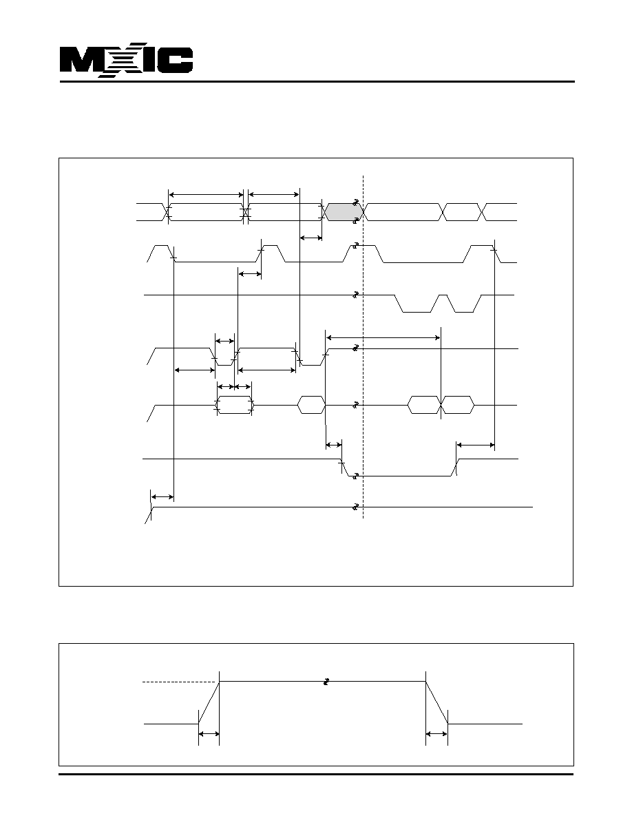
46
P/N:PM1170
REV. 0.04, JUL. 11, 2005
MX29LA128M T/B
ERASE/PROGRAM OPERATION
Figure 4. AUTOMATIC PROGRAM TIMING WAVEFORMS
Figure 5. ACCELERATED PROGRAM TIMING DIAGRAM
ACC
tVHH
VHH
VIL or VIH
VIL or VIH
tVHH
tWC
Address
OE#
CE#
A0h
XXXh
PA
PD
Status
DOUT
PA
PA
Note :
1.PA=Program Address, PD=Program Data, DOUT is the true data the program address
tAS
tAH
tCH
tWP
tDS
tDH
tWHWH1
Read Status Data (last two cycle)
Program Command Sequence(last two cycle)
tBUSY
tRB
tCS
tWPH
tVCS
WE#
Data
RY/BY#
VCC
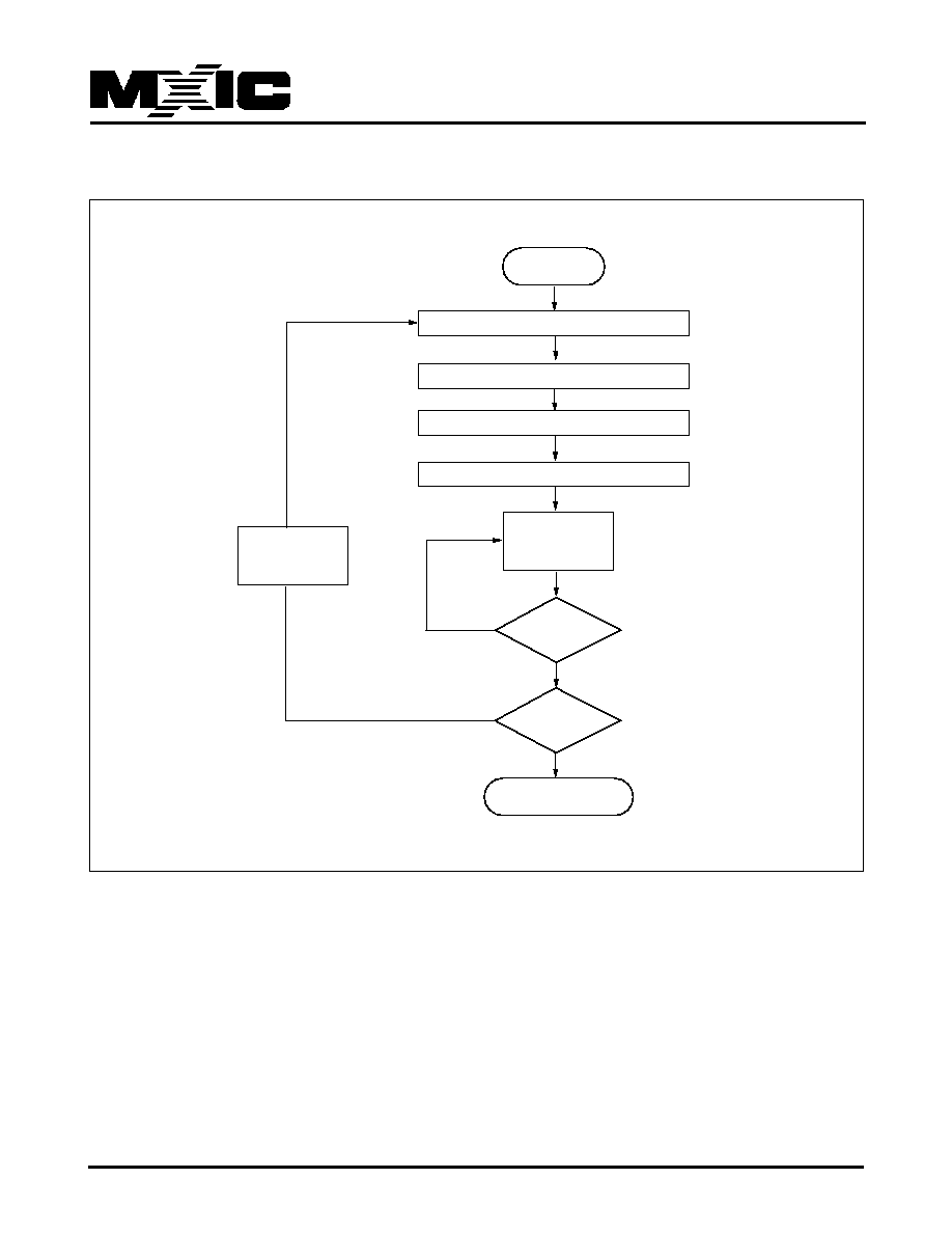
47
P/N:PM1170
REV. 0.04, JUL. 11, 2005
MX29LA128M T/B
Figure 6. AUTOMATIC PROGRAMMING ALGORITHM FLOWCHART
START
Write Data AAH Address 555H
Write Data 55H Address 2AAH
Write Program Data/Address
Write Data A0H Address 555H
YES
Verify Word Ok ?
YES
Auto Program Completed
Data Poll
from system
Increment
Address
Last Address ?
No
No
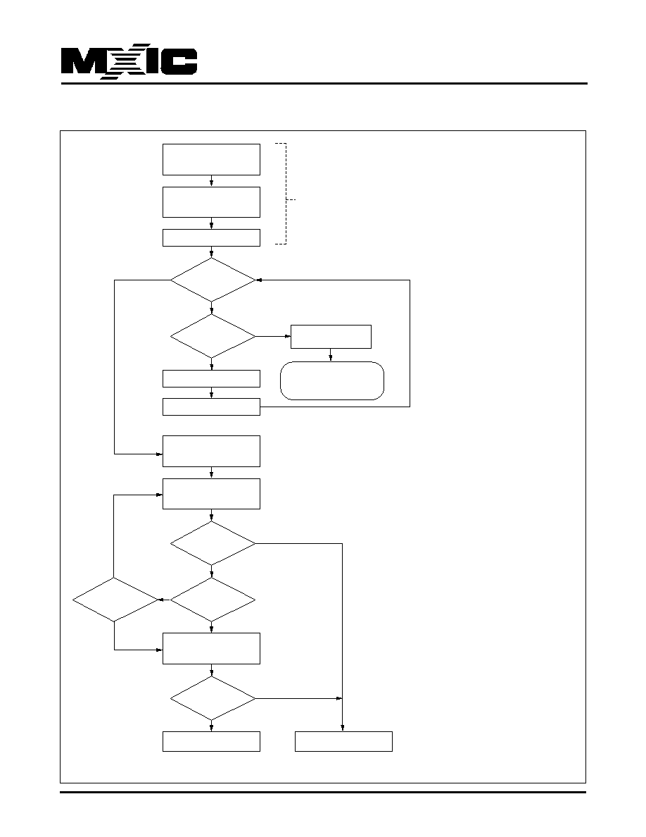
48
P/N:PM1170
REV. 0.04, JUL. 11, 2005
MX29LA128M T/B
Figure 7. WRITE BUFFER PROGRAMMING ALGORITHM FLOWCHART
Notes:
1. When Sector Address is specified, any address in
the selected sector is acceptable. However, when
loading Write-Buffer address locations with data, all
addresses must fall within the selected Write-Buffer
Page.
2. Q7 may change simultaneously with Q5.
Therefore, Q7 should be verified.
3. If this flowchart location was reached because Q5=
"1" then the device FAILED. If this flowchart location
was reached because Q1="1", then the Write to
Buffer operation was ABORTED. In either case, the
proper reset command must be written before the
device can begin another operation. If Q1=1, write
the Write-Buffer-Programming-Abort-Reset com-
mand. If Q5=1, write the Reset command.
4. See Table 3 for command sequences required for
write buffer programming.
Write "Write to Buffer"
command and
Sector Address
Write number of addresses
to program minus 1(WC)
and Sector Address
Part of "Write to Buffer"
Command Sequence
Write program buffer
to flash sector address
Read Q7~Q0 at Last
Loaded Address
Read Q7~Q0 with address
= Last Loaded Address
FAIL or ABORT
PASS
Write first address/data
Write next address/data pair
Write to a different
sector address
Write to buffer ABORTED.
Must write "Write-to-buffer
Abort Reset" command sequence
to return to read mode.
WC = WC - 1
WC = 0 ?
Abort Write to
Buffer Operation ?
Q7 = Data ?
Q5 = 1 ?
Q1 = 1 ?
Q7 and Q15 = Data ?
Yes
Yes
Yes
Yes
Yes
Yes
(Note 2)
(Note 1)
(Note 3)
No
No
No
No
No
No

49
P/N:PM1170
REV. 0.04, JUL. 11, 2005
MX29LA128M T/B
Figure 8. PROGRAM SUSPEND/RESUME FLOWCHART
Program Operation
or Write-to-Buffer
Sequence in Progress
Write address/data
XXXh/B0h
Write Program Suspend
Command Sequence
Command is also valid for
Erase-suspended-program
operations
Autoselect and Secured Sector
read operations are also allowed
Data cannot be read from erase-or
program-suspended sectors
Write Program Resume
Command Sequence
Read data as
required
Write address/data
XXXh/30h
Device reverts to
operation prior to
Program Suspend
Wait 15us
Done reading ?
No
Yes
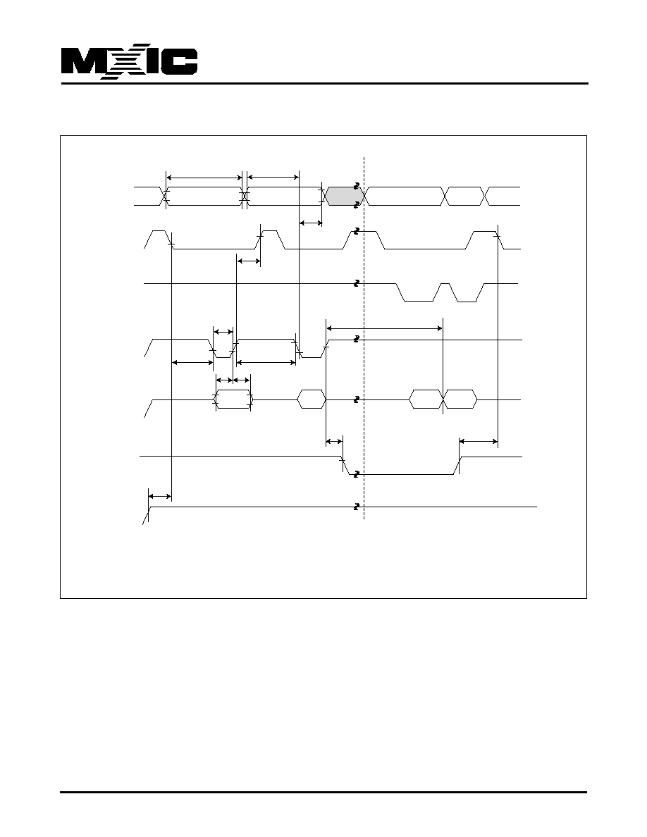
50
P/N:PM1170
REV. 0.04, JUL. 11, 2005
MX29LA128M T/B
Figure 9. AUTOMATIC CHIP/SECTOR ERASE TIMING WAVEFORM
tWC
Address
OE#
CE#
55h
2AAh
SA
30h
In
Progress Complete
VA
VA
Note :
1.SA=sector address(for Sector Erase), VA=Valid Address for reading status data(see "Write Operation Status").
tAS
tAH
555h for chip erase
tCH
tWP
tDS
tDH
tWHWH2
Read Status Data
Erase Command Sequence(last two cycle)
tBUSY
tRB
tCS
tWPH
10 for Chip Erase
tVCS
WE#
Data
RY/BY#
VCC
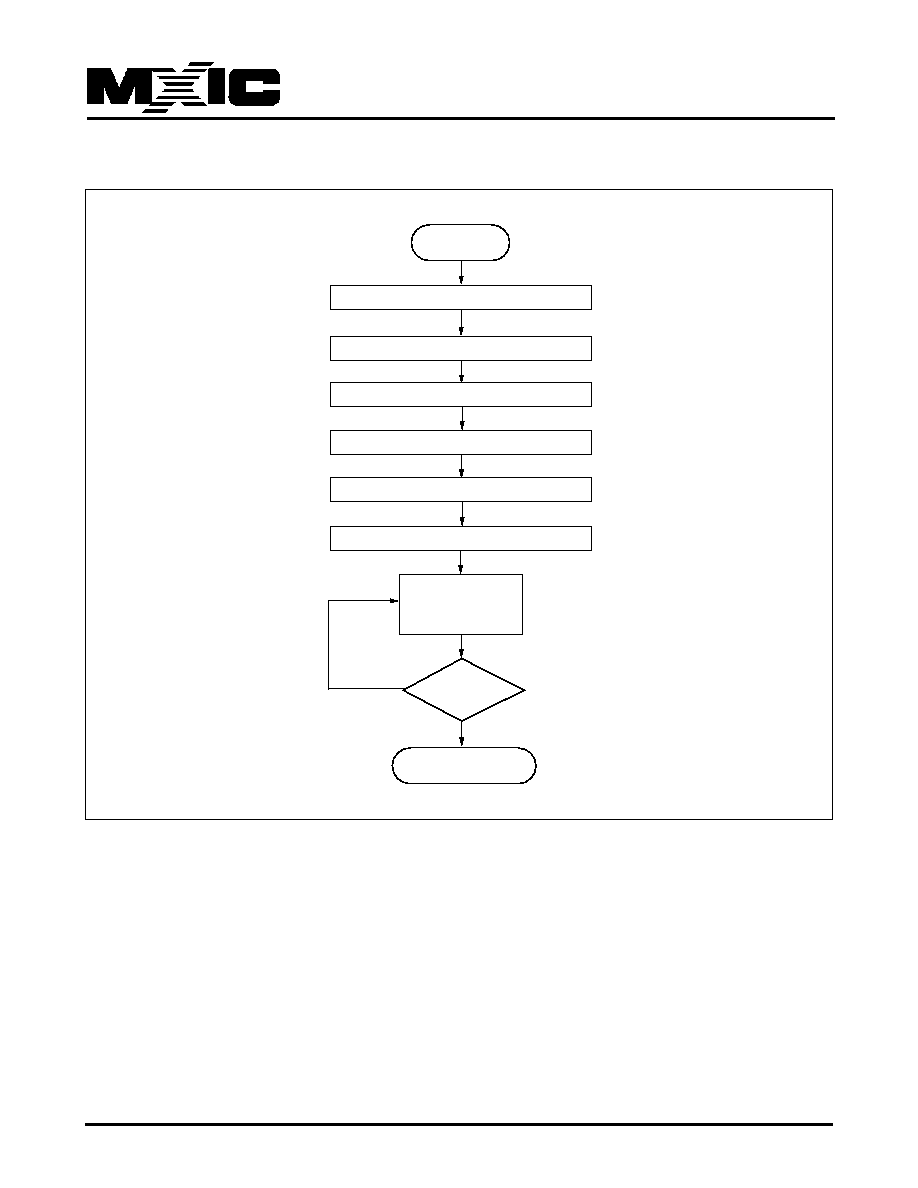
51
P/N:PM1170
REV. 0.04, JUL. 11, 2005
MX29LA128M T/B
Figure 10. AUTOMATIC CHIP ERASE ALGORITHM FLOWCHART
START
Write Data AAH Address 555H
Write Data 55H Address 2AAH
Write Data AAH Address 555H
Write Data 80H Address 555H
YES
Write Data 10H Address 555H
Write Data 55H Address 2AAH
DATA = FFh ?
YES
Auto Erase Completed
Data Poll
from system
No
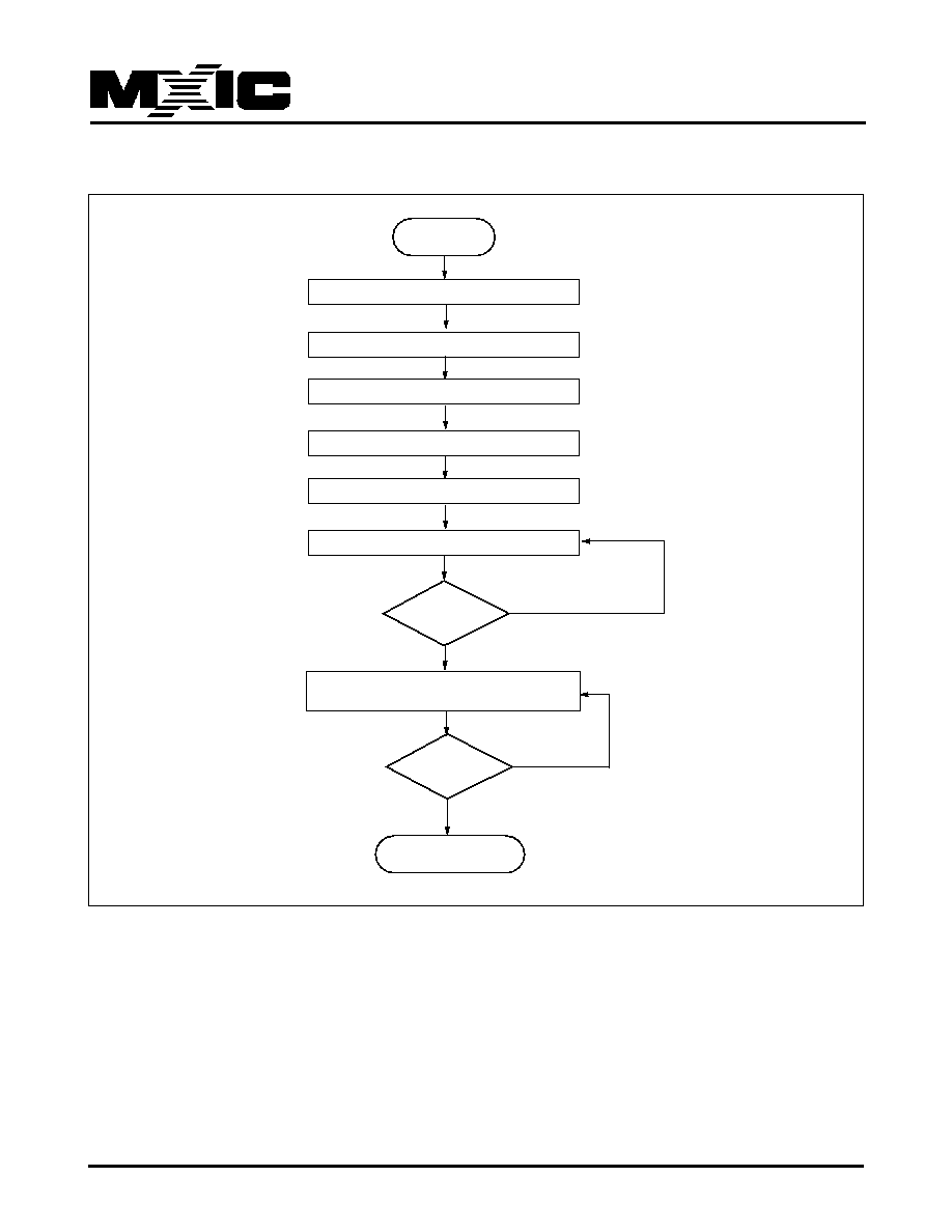
52
P/N:PM1170
REV. 0.04, JUL. 11, 2005
MX29LA128M T/B
Figure 11. AUTOMATIC SECTOR ERASE ALGORITHM FLOWCHART
START
Write Data AAH Address 555H
Write Data 55H Address 2AAH
Write Data AAH Address 555H
Write Data 80H Address 555H
Write Data 30H Sector Address
Write Data 55H Address 2AAH
Auto Sector Erase Completed
Data Poll from System
YES
NO
Data=FFh?
Last Sector
to Erase ?
NO
YES
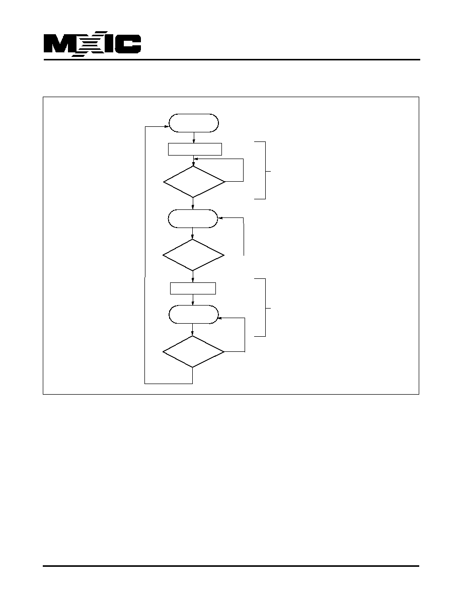
53
P/N:PM1170
REV. 0.04, JUL. 11, 2005
MX29LA128M T/B
Figure 12. ERASE SUSPEND/RESUME FLOWCHART
START
Write Data B0H
Toggle Bit checking Q6
not toggled
ERASE SUSPEND
YES
NO
Write Data 30H
Continue Erase
Reading or
Programming End
Read Array or
Program
Another
Erase Suspend ?
NO
YES
YES
NO
ERASE RESUME
54
P/N:PM1170
REV. 0.04, JUL. 11, 2005
MX29LA128M T/B
AC CHARACTERISTICS
Alternate CE# Controlled Erase and Program Operations
Parameter
Speed Options
Std.
Description
90R
100
Unit
tWC
Write Cycle Time (Note 1)
Min
90
100
ns
tAS
Address Setup Time
Min
0
ns
tAH
Address Hold Time
Min
45
ns
tDS
Data Setup Time
Min
35
ns
tDH
Data Hold Time
Min
0
ns
tGHEL
Read Recovery Time Before Write
Min
0
ns
(OE# High to WE# Low)
tWS
WE# Setup Time
Min
0
ns
tWH
WE# Hold Time
Min
0
ns
tCP
CE# Pulse Width
Min
35
ns
tCPH
CE# Pulse Width High
Min
25
ns
Write Buffer Program Operation (Notes 2,3)
Typ
240
us
Single Word/Byte Program
Byte
Typ
60
us
tWHWH1
Operation (Notes 2,5)
Word
Typ
60
us
Accelerated Single Word/Byte
Byte
Typ
54
us
Programming Operation (Notes 2,5)
Word
Typ
54
us
tWHWH2
Sector Erase Operation (Note 2)
Typ
0.5
sec
tRH
RESET HIGH Time Before Write (Note 1)
Min
50
ns
tPOLL
Program Valid Before Status Polling (Note 6)
Max
4
us
Notes:
1. Not 100% tested.
2. See the "Erase And Programming Performance" section for more information.
3. For 1-16 words/1-32 bytes programmed.
4. Effective write buffer specification is based upon a 16-word/32-byte write buffer operation.
5. Word/Byte programming specification is based upon a single word/byte programming operation not utilizing the
write buffer.
6. When using the program suspend/resume feature, if the suspend command is issued within tPOLL, tPOLL must be
fully re-applied upon resuming the programming operation. If the suspend command is issued after tPOLL, tPOLL is
not required again prior to reading the status bits upon resuming.
TA=-40
∞∞
∞∞
∞
C to 85
∞∞
∞∞
∞
C, VCC=2.7V~3.6V
(VCC=3.0V~3.6V for 90R)
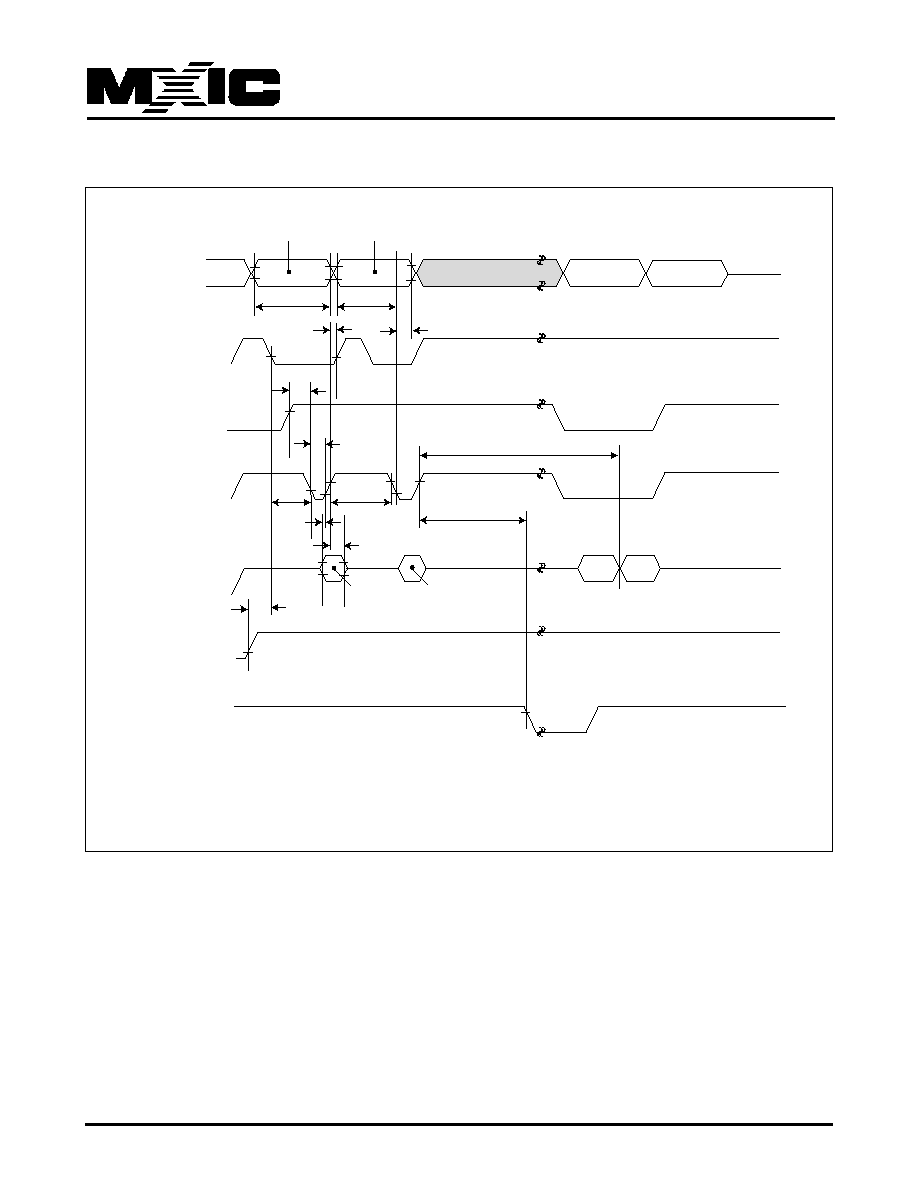
55
P/N:PM1170
REV. 0.04, JUL. 11, 2005
MX29LA128M T/B
Figure 13. CE# CONTROLLED PROGRAM TIMING WAVEFORM
tWC
tWH
tGHEL
tWHWH1 or 2
tCP
Address
WE#
OE#
CE#
Data
Q7
PA
Data# Polling
DOUT
RESET#
RY/BY#
NOTES:
1.PA=Program Address, PD=Program Data, DOUT=Data Out, Q7=complement of data written to device.
2.Figure indicates the last two bus cycles of the command sequence.
tAH
tAS
PA for program
SA for sector erase
555 for chip erase
tRH
tDH
tDS
tWS
A0 for program
55 for erase
tCPH
tBUSY
PD for program
30 for sector erase
10 for chip erase
555 for program
2AA for erase
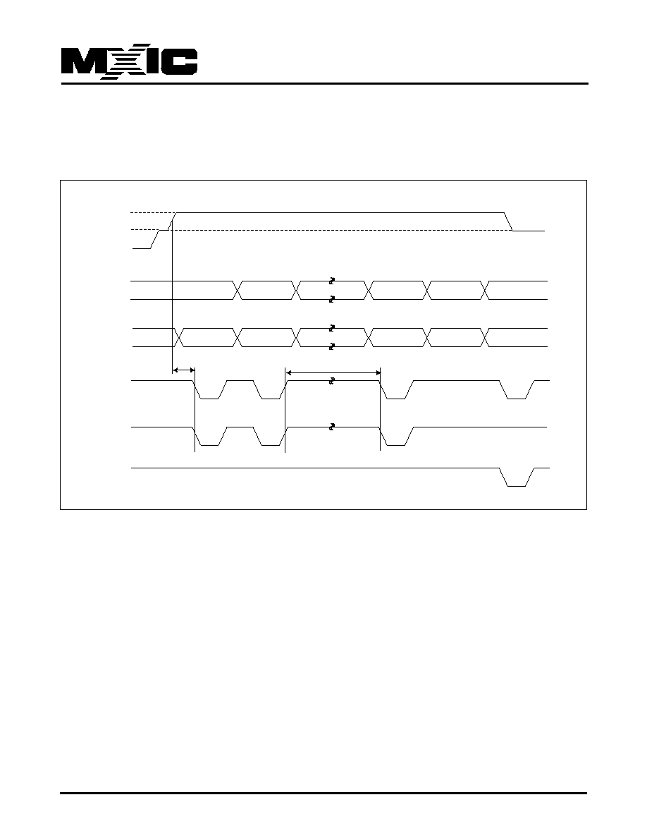
56
P/N:PM1170
REV. 0.04, JUL. 11, 2005
MX29LA128M T/B
SECTOR GROUP PROTECT/CHIP UNPROTECT
Figure 14. Sector Group Protect / Chip Unprotect Waveform (RESET# Control)
Note: For sector group protect A6=0, A1=1, A0=0. For chip unprotect A6=1, A1=1, A0=0
Sector Group Protect:150us
Chip Unprotect:15ms
1us
VID
VIH
Data
SA, A6
A1, A0
CE#
WE#
OE#
Valid*
Valid*
Status
Valid*
Sector Group Protect or Chip Unprotect
40h
60h
60h
Verify
RESET#
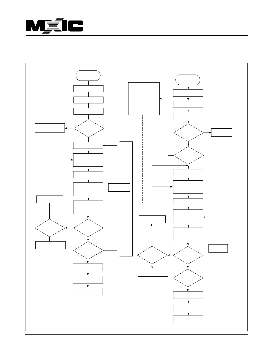
57
P/N:PM1170
REV. 0.04, JUL. 11, 2005
MX29LA128M T/B
Figure 15. IN-SYSTEM SECTOR GROUP PROTECT/CHIP UNPROTECT ALGORITHMS WITH
RESET#=VID
START
PLSCNT=1
RESET#=VID
Wait 1us
Set up sector address
Sector Protect:
Write 60h to sector
address with
A6=0, A1=1, A0=0
Wait 150us
Verify Sector Protect:
Write 40h to sector
address with
A6=0, A1=1, A0=0
Read from
sector address
with
A6=0, A1=1, A0=0
Reset
PLSCNT=1
Remove VID from RESET#
Write reset command
Sector Protect
Algorithm
Chip Unprotect
Algorithm
Sector Protect complete
Remove VID from RESET#
Write reset command
Sector Unprotect complete
Device failed
Temporary Sector
Unprotect Mode
Increment PLSCNT
Increment PLSCNT
First Write
Cycle=60h?
Set up first sector address
Protect all sectors:
The indicated portion of
the sector protect algorithm
must be performed
for all unprotected sectors
prior to issuing the first
sector unprotect address
Sector Unprotect:
Write 60h to sector
address with
A6=1, A1=1, A0=0
Wait 15 ms
Verify Sector Unprotect:
Write 40h to sector
address with
A6=1, A1=1, A0=0
Read from
sector address
with
A6=1, A1=1, A0=0
Data=01h?
PLSCNT=25?
Device failed
START
PLSCNT=1
RESET#=VID
Wait 1us
First Write
Cycle=60h?
All sectors
protected?
Data=00h?
PLSCNT=1000?
Last sector
verified?
Yes
Yes
Yes
No
No
No
Yes
Yes
Yes
Yes
Yes
Yes
No
No
No
No
No
No
Protect another
sector?
Reset
PLSCNT=1
Temporary Sector
Unprotect Mode
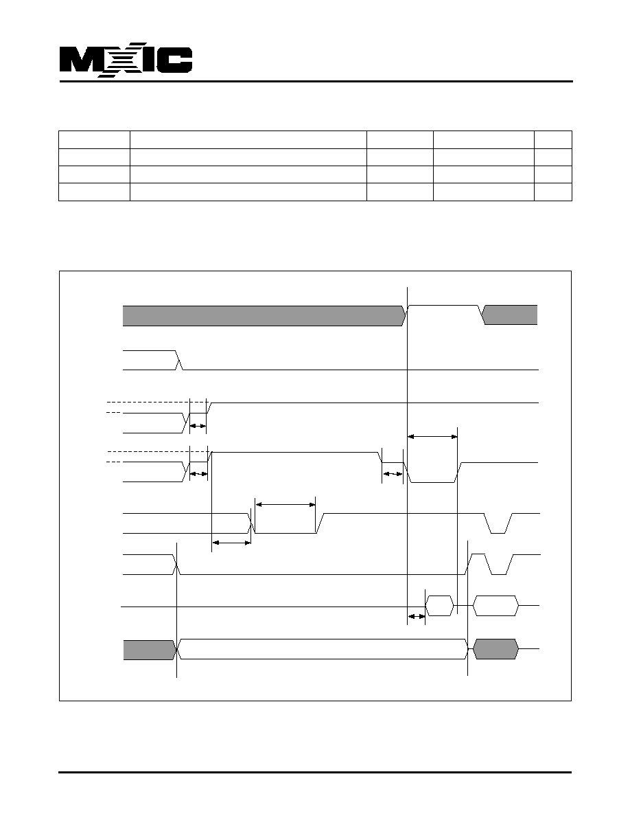
58
P/N:PM1170
REV. 0.04, JUL. 11, 2005
MX29LA128M T/B
Figure 16. SECTOR GROUP PROTECT TIMING WAVEFORM (A9, OE# Control)
Parameter
Description
Test Setup
All Speed Options
Unit
tVLHT
Voltage transition time
Min.
4
us
tWPP1
Write pulse width for sector group protect
Min.
100
ns
tOESP
OE# setup time to WE# active
Min.
4
us
AC CHARACTERISTICS
tOE
Data
OE#
WE#
12V
3V
12V
3V
CE#
A9
A1
A6
tOESP
tWPP 1
tVLHT
tVLHT
tVLHT
Verify
01H
F0H
A21-A16
Sector Address
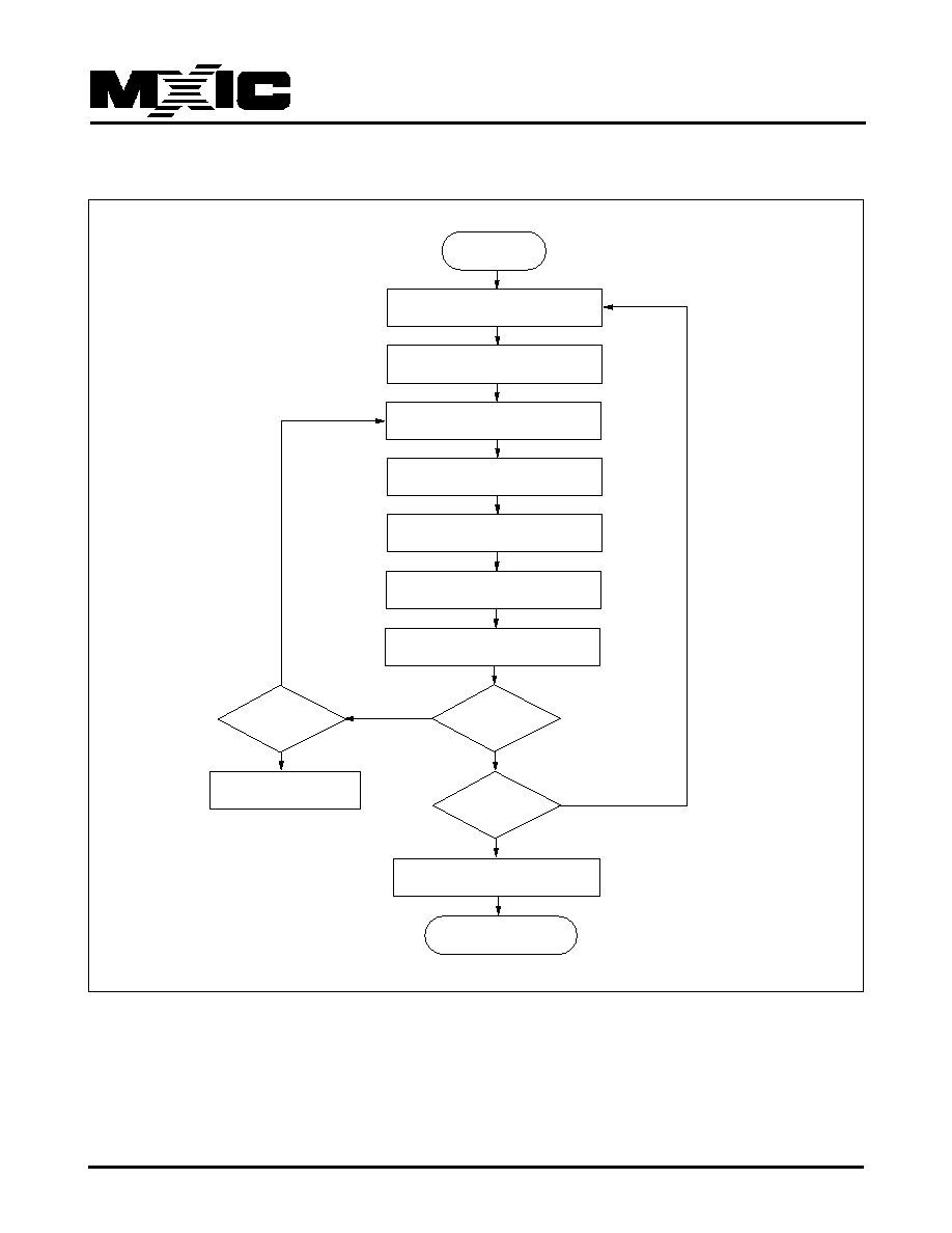
59
P/N:PM1170
REV. 0.04, JUL. 11, 2005
MX29LA128M T/B
Figure 17. SECTOR GROUP PROTECTION ALGORITHM (A9, OE# Control)
START
Set Up Sector Addr
PLSCNT=1
Sector Protection
Complete
Data=01H?
Yes
.
OE#=VID, A9=VID, CE#=VIL
A6=VIL
Activate WE# Pulse
Time Out 150us
Set WE#=VIH, CE#=OE#=VIL
A9 should remain VID
Read from Sector
Addr=SA, A1=1
Protect Another
Sector?
Remove VID from A9
Write Reset Command
Device Failed
PLSCNT=32?
Yes
No
No
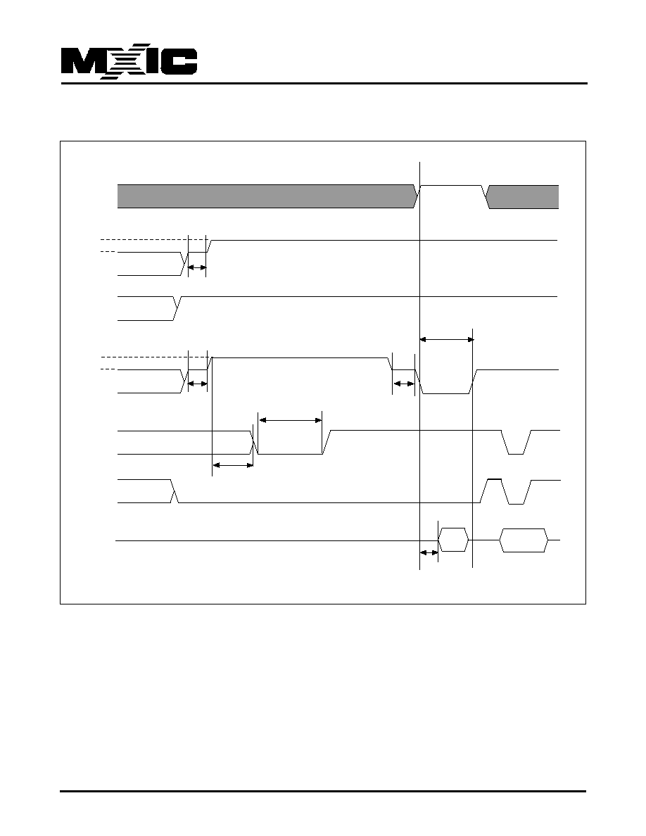
60
P/N:PM1170
REV. 0.04, JUL. 11, 2005
MX29LA128M T/B
Figure 18. CHIP UNPROTECT TIMING WAVEFORM (A9, OE# Control)
tOE
Data
OE#
WE#
12V
3V
12V
3V
CE#
A9
A1
tOESP
tWPP 2
tVLHT
tVLHT
tVLHT
Verify
00H
A6
F0H
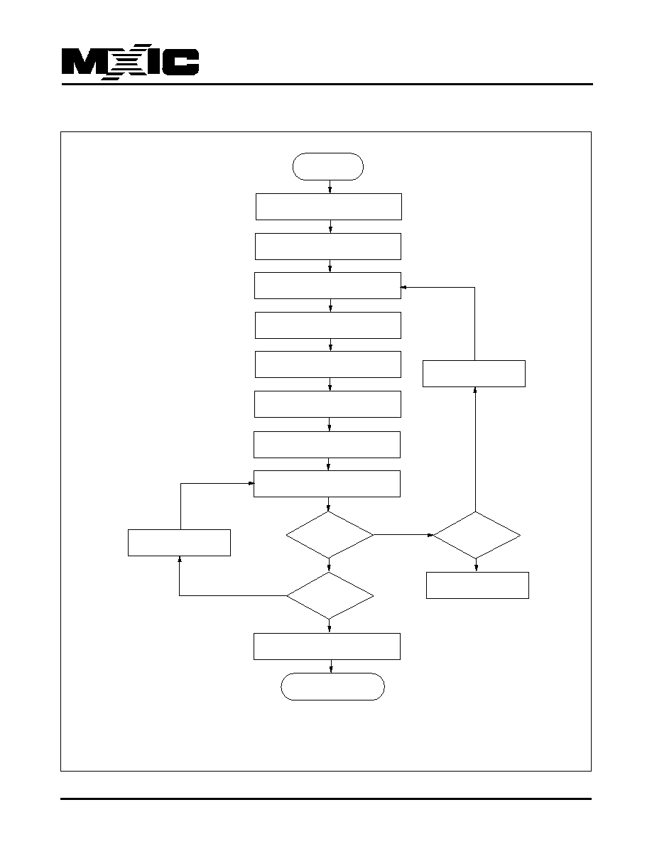
61
P/N:PM1170
REV. 0.04, JUL. 11, 2005
MX29LA128M T/B
Figure 19. CHIP UNPROTECT FLOWCHART (A9, OE# Control)
START
Protect All Sectors
PLSCNT=1
Chip Unprotect
Complete
Data=00H?
Yes
Set OE#=A9=VID
CE#=VIL, A6=1
Activate WE# Pulse
Time Out 15ms
Set OE#=CE#=VIL
A9=VID, A1=1
Set Up First Sector Addr
All sectors have
been verified?
Remove VID from A9
Write Reset Command
Device Failed
PLSCNT=1000?
No
Increment
PLSCNT
No
Read Data from Device
Yes
Yes
No
Increment
Sector Addr
* It is recommended before unprotect whole chip, all sectors should be protected in advance.
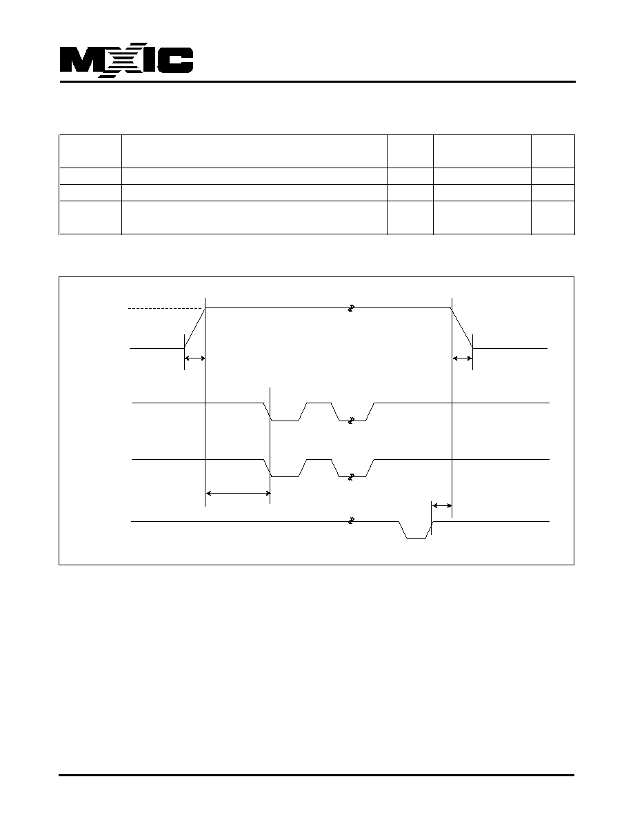
62
P/N:PM1170
REV. 0.04, JUL. 11, 2005
MX29LA128M T/B
Figure 20. TEMPORARY SECTOR GROUP UNPROTECT WAVEFORMS
AC CHARACTERISTICS
Parameter
Description
Test
All Speed Options Unit
Setup
tVIDR
VID Rise and Fall Time (see Note)
Min
500
ns
tRSP
RESET# Setup Time for Temporary Sector Unprotect
Min
4
us
tRRB
RESET# Hold Time from RY/BY# High for Temporary
Min
4
us
Sector Group Unprotect
RESET#
CE#
WE#
RY/BY#
tVIDR
12V
0 or 3V
VIL or VIH
tRSP
tVIDR
Program or Erase Command Sequence
tRRB
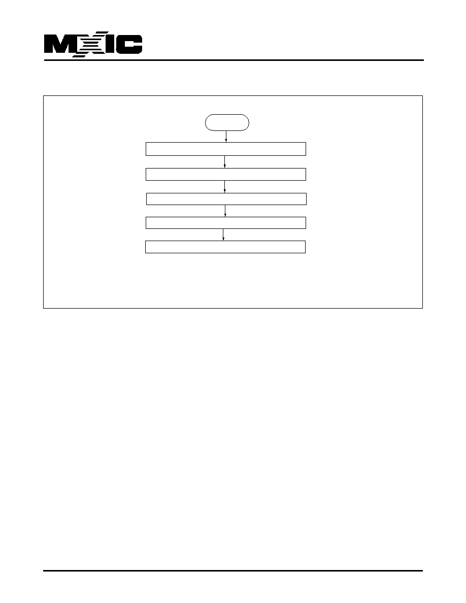
63
P/N:PM1170
REV. 0.04, JUL. 11, 2005
MX29LA128M T/B
Figure 21. TEMPORARY SECTOR GROUP UNPROTECT FLOWCHART
Start
RESET# = VID (Note 1)
Perform Erase or Program Operation
RESET# = VIH
Temporary Sector Unprotect Completed(Note 2)
Operation Completed
2. All previously protected sectors are protected again.
Notes : 1. All protected sectors are temporary unprotected.
VID=11.5V~12.5V
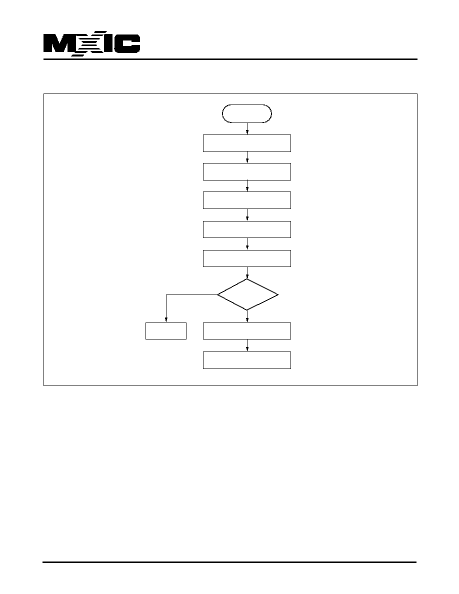
64
P/N:PM1170
REV. 0.04, JUL. 11, 2005
MX29LA128M T/B
Figure 22. SECURED SILICON SECTOR PROTECTED ALGORITHMS FLOWCHART
START
Enter Secured Silicon Sector
Data = 01h ?
No
Yes
Wait 1us
First Wait Cycle Data=60h
Second Wait Cycle Data=60h
A6=0, A1=1, A0=0
Wait 300us
Write Reset Command
Device Failed
Secured Sector Protect Complete
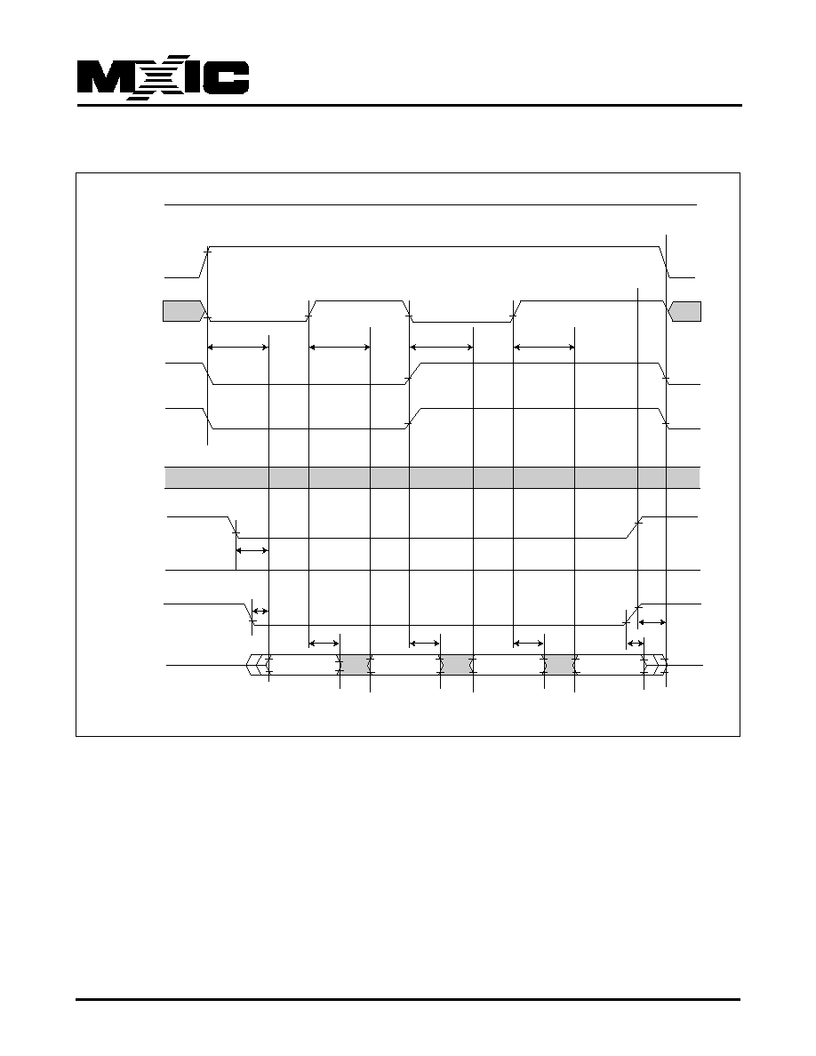
65
P/N:PM1170
REV. 0.04, JUL. 11, 2005
MX29LA128M T/B
Figure 23. SILICON ID READ TIMING WAVEFORM
tACC
tCE
tACC
tOE
tOH
tOH
tDF
DATA OUT
Manufacturer ID
Device ID
Cycle 1
Device ID
Cycle 2
Device ID
Cycle 3
VID
VIH
VIL
ADD
A9
ADD
CE#
A1
OE#
WE#
ADD
A0
DATA OUT
DATA OUT
DATA OUT
DATA
Q0-Q15
VCC
3V
VIH
VIL
VIH
VIL
VIH
VIL
A2
VIH
VIL
VIH
VIL
VIH
VIL
VIH
VIL
VIH
VIL
tACC
tACC
tOH
tOH
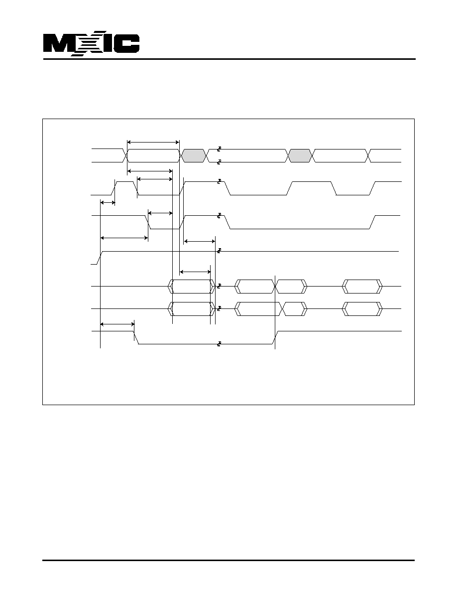
66
P/N:PM1170
REV. 0.04, JUL. 11, 2005
MX29LA128M T/B
WRITE OPERATION STATUS
Figure 24. DATA# POLLING TIMING WAVEFORMS (DURING AUTOMATIC ALGORITHMS)
Note :
VA=Valid address. Figure shows are first status cycle after command sequence, last status read cycle, and array data raed cycle.
tDF
tCE
tCH
tOE
tOEH
tACC
tRC
tOH
Address
CE#
OE#
WE#
Q7
Q0-Q6
RY/BY#
tBUSY
Status Data
Status Data
Status Data
Complement
True
Valid Data
VA
VA
VA
High Z
High Z
Valid Data
True
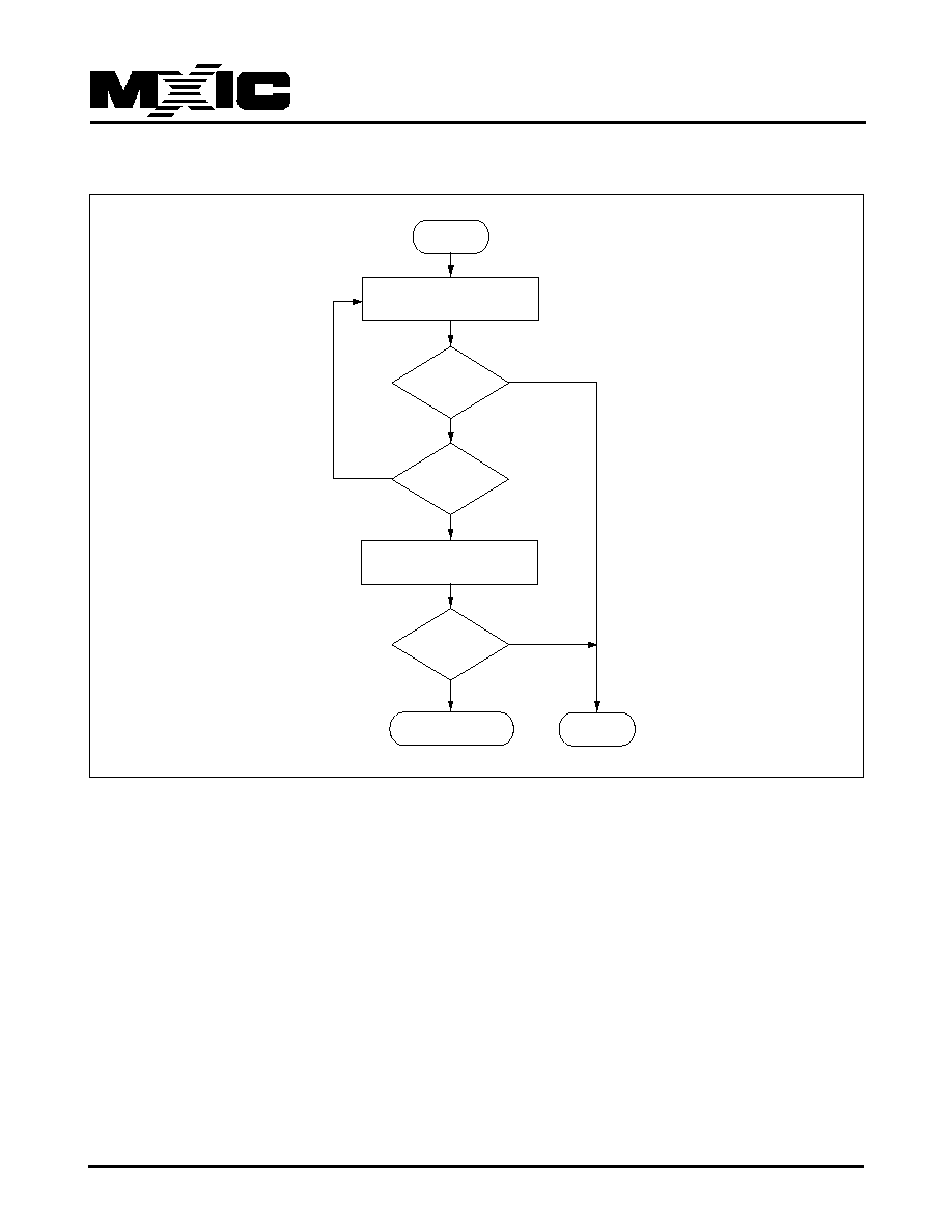
67
P/N:PM1170
REV. 0.04, JUL. 11, 2005
MX29LA128M T/B
Figure 25. DATA# POLLING ALGORITHM
Notes:
1.VA=valid address for programming.
2.Q7 should be rechecked even Q5="1" because Q7 may change simultaneously with Q5.
Read Q7~Q0
Add.=VA(1)
Read Q7~Q0
Add.=VA
Start
Q7 = Data ?
Q5 = 1 ?
Q7 = Data ?
FAIL
Pass
No
No
(2)
No
Yes
Yes
Yes
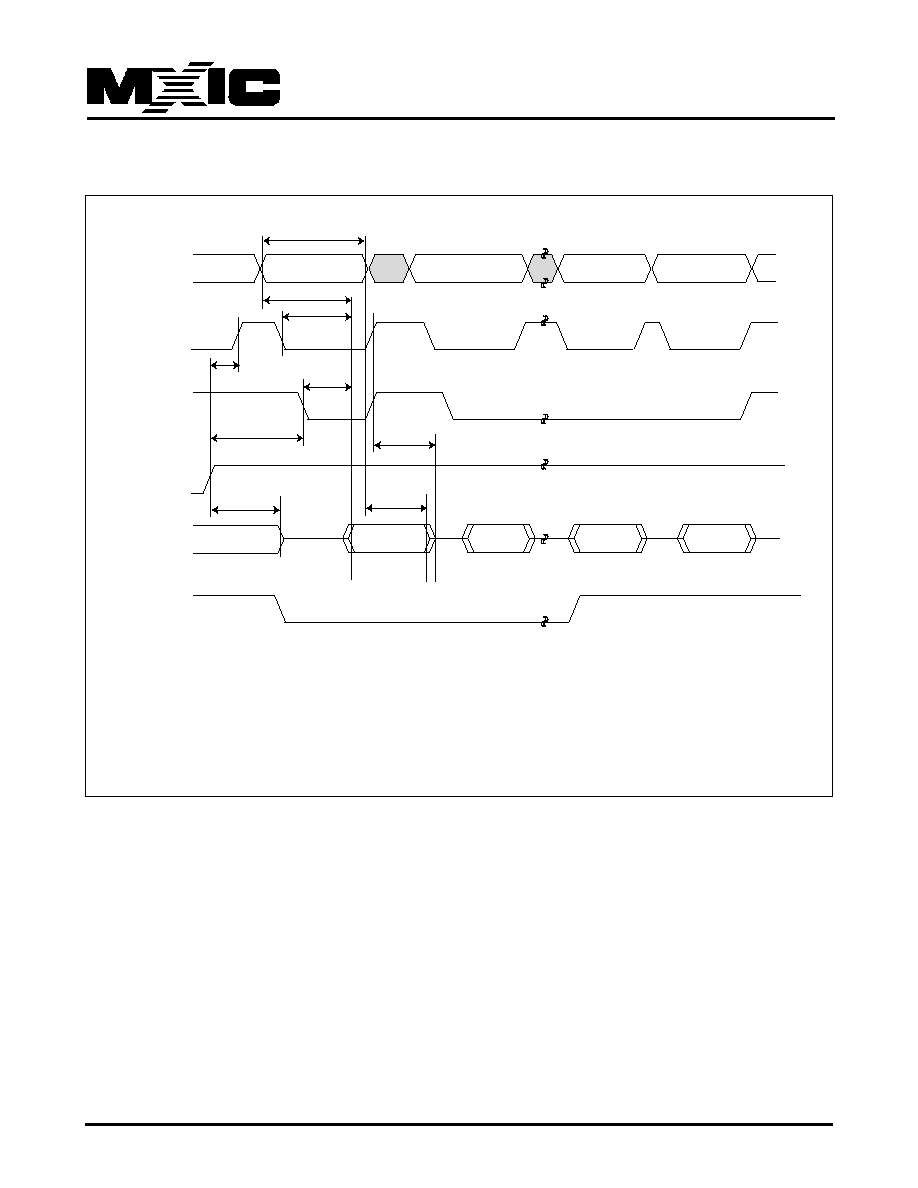
68
P/N:PM1170
REV. 0.04, JUL. 11, 2005
MX29LA128M T/B
Figure 26. TOGGLE BIT TIMING WAVEFORMS (DURING AUTOMATIC ALGORITHMS)
Note :
VA=Valid address; not required for Q6. Figure shows first two status cycle after command sequence, last status read cycle, and
array data read cycle.
tDF
tCE
tCH
tOE
tOEH
tACC
tRC
tOH
Address
CE#
OE#
WE#
Q6/Q2
RY/BY#
tDH
Valid Status
Valid Status
(first read)
Valid Status
(second read)
(stops toggling)
Valid Data
VA
VA
VA
VA
Valid Data
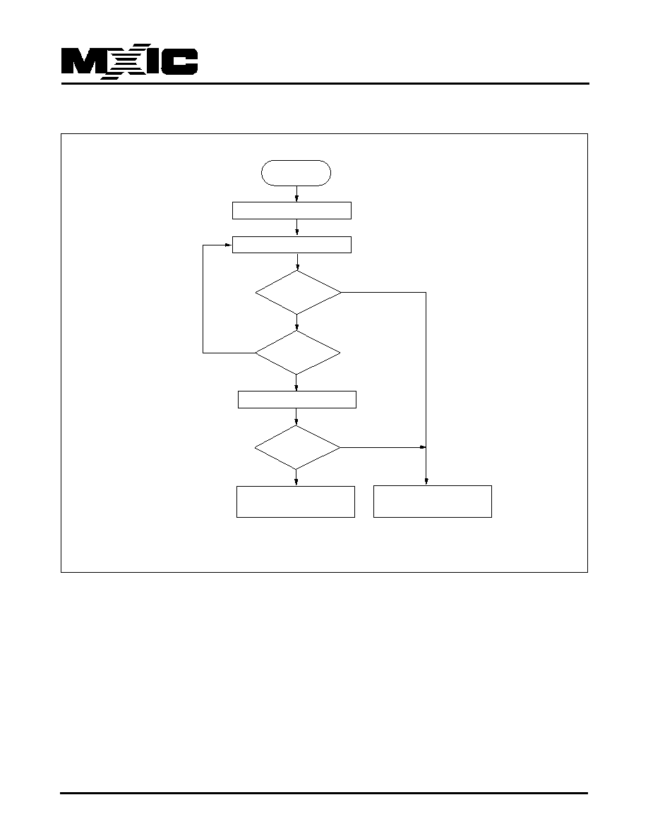
69
P/N:PM1170
REV. 0.04, JUL. 11, 2005
MX29LA128M T/B
START
Read Q7~Q0
Read Q7~Q0
YES
NO
Toggle Bit Q6
=Toggle?
Q5=1?
YES
NO
(Note 1)
Read Q7~Q0 Twice
(Note 1,2)
Toggle Bit Q6=
Toggle?
Program/Erase Operation Not
Complete, Write Reset Command
YES
Program/Erase Operation Complete
Figure 27. TOGGLE BIT ALGORITHM
Notes :
1. Read toggle bit twice to determine whether or not it is toggling.
2. Recheck toggle bit because it may stop toggling as Q5 changes to "1".
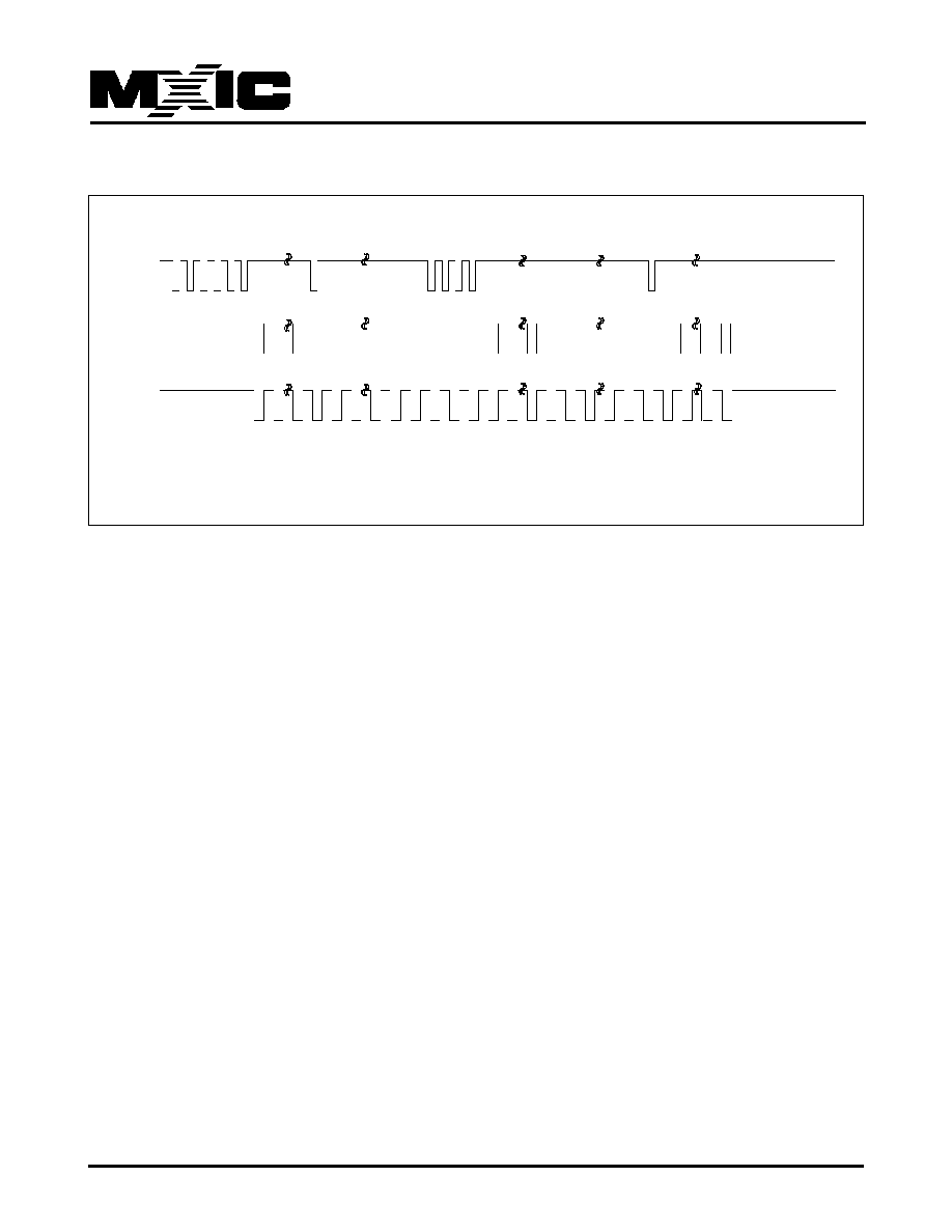
70
P/N:PM1170
REV. 0.04, JUL. 11, 2005
MX29LA128M T/B
Figure 28. Q6 versus Q2
Note :
The system can use OE# or CE# to toggle Q2/Q6, Q2 toggles only when read at an address within an erase-suspended
WE#
Enter Embedded
Erasing
Erase
Suspend
Enter Erase
Suspend Program
Erase
Suspend
Program
Erase Suspend
Read
Erase Suspend
Read
Erase
Erase
Resume
Erase
Complete
Erase
Q6
Q2
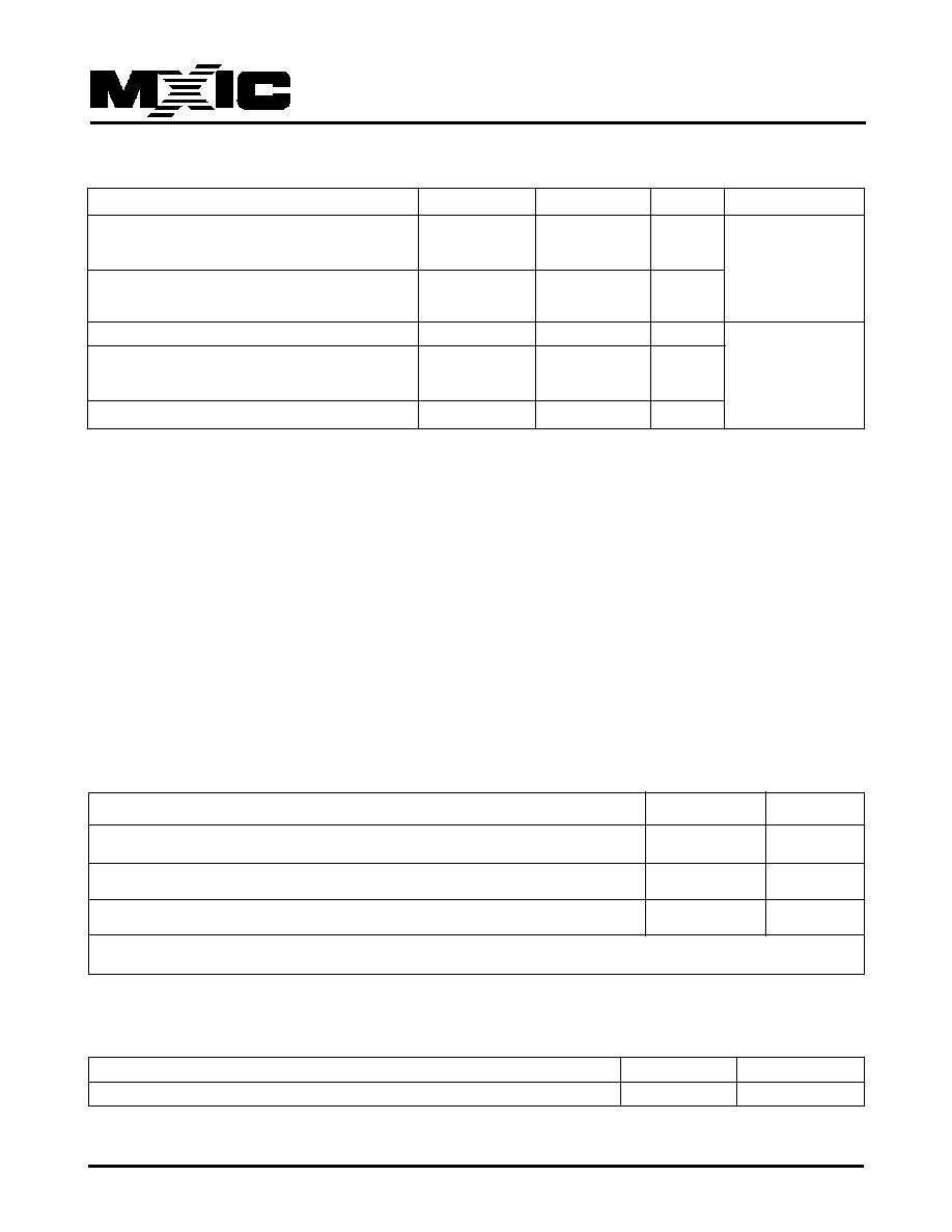
71
P/N:PM1170
REV. 0.04, JUL. 11, 2005
MX29LA128M T/B
MIN.
MAX.
Input Voltage with respect to GND on all pins except I/O pins
-1.0V
13.5V
Input Voltage with respect to GND on all I/O pins
-1.0V
VCC + 1.0V
Current
-100mA
+100mA
Includes all pins except VCC. Test conditions: VCC = 3.0V, one pin at a time.
LATCH-UP CHARACTERISTICS
ERASE AND PROGRAMMING PERFORMANCE (1)
Notes:
1. Typical program and erase times assume the following conditions: 25
∞
C, 3.0V VCC. Programming specifications
assume checkboard data pattern.
2. Maximum values are measured at VCC = 3.0 V, worst case temperature. Maximum values are valid up to and
including 100,000 program/erase cycles.
3. Word/Byte programming specification is based upon a single word/byte programming operation not utilizing the
write buffer.
4. For 1-16 words or 1-32 bytes programmed in a single write buffer programming operation.
5. Effective write buffer specification is calculated on a per-word/per-byte basis for a 16-word/32-byte write buffer
operation.
6. In the pre-programming step of the Embedded Erase algorithm, all bits are programmed to 00h before erasure.
7. System-level overhead is the time required to execute the command sequence(s) for the program command. See
Tables 3 for further information on command definitions.
8. The device has a minimum erase and program cycle endurance of 100,000 cycles.
Parameter
Min
Unit
Minimum Pattern Data Retention Time
20
Years
DATA RETENTION
PARAMETER
Typ (Note 1)
Max (Note 2)
Unit
Comments
Sector Erase Time
0.5
2
sec
Excludes 00h
programming
Chip Erase Time
128
256
sec
prior to erasure
Note 6
Total Write Buffer Program Time (Note 4)
240
us
Excludes
Total Accelerated Effective Write Buffer
200
us
system level
Program Time (Note 4)
overhead
Chip Program Time
126
sec
Note 7
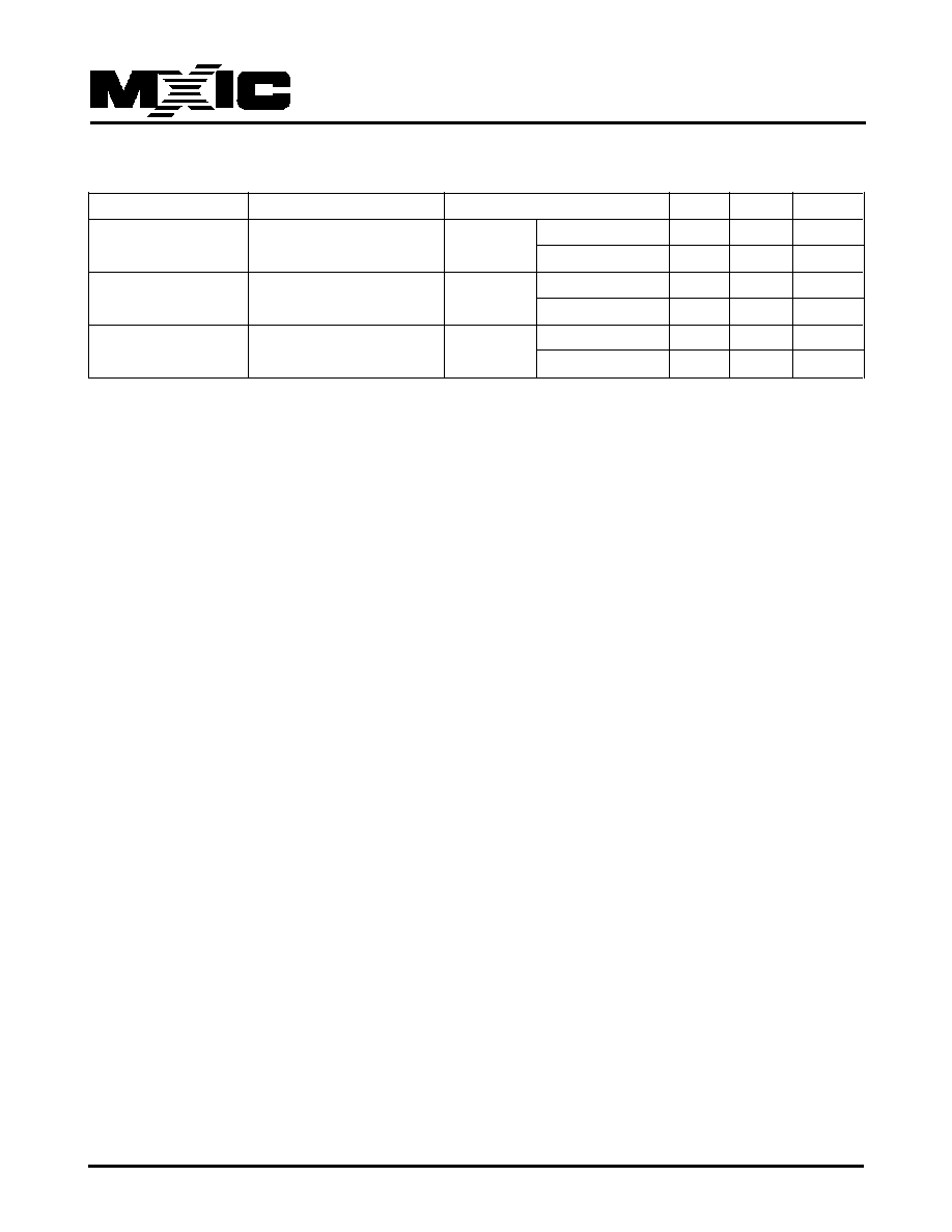
72
P/N:PM1170
REV. 0.04, JUL. 11, 2005
MX29LA128M T/B
Parameter Symbol
Parameter Description
Test Set
TYP
MAX
UNIT
CIN
Input Capacitance
VIN=0
TSOP
6
7.5
pF
CSP
4.2
5.0
pF
COUT
Output Capacitance
VOUT=0
TSOP
8.5
12
pF
CSP
5.4
6.5
pF
CIN2
Control Pin Capacitance
VIN=0
TSOP
7.5
9
pF
CSP
3.9
4.7
pF
TSOP PIN AND BGA PACKAGE CAPACITANCE
Notes:
1. Sampled, not 100% tested.
2. Test conditions TA=25
∞
C, f=1.0MHz
73
P/N:PM1170
REV. 0.04, JUL. 11, 2005
MX29LA128M T/B
ORDERING INFORMATION
PLASTIC PACKAGE
PART NO.
ACCESS TIME
PACKAGE
Remark
(ns)
MX29LA128MTTC-90R
90
56 Pin TSOP
(Normal Type)
MX29LA128MTTC-10
100
56 Pin TSOP
(Normal Type)
MX29LA128MBTC-90R
90
56 Pin TSOP
(Normal Type)
MX29LA128MBTC-10
100
56 Pin TSOP
(Normal Type)
MX29LA128MTTI-90R
90
56 Pin TSOP
(Normal Type)
MX29LA128MTTI-10
100
56 Pin TSOP
(Normal Type)
MX29LA128MBTI-90R
90
56 Pin TSOP
(Normal Type)
MX29LA128MBTI-10
100
56 Pin TSOP
(Normal Type)
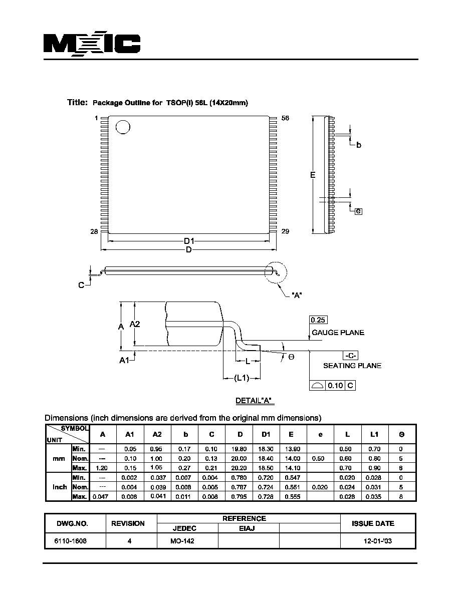
74
P/N:PM1170
REV. 0.04, JUL. 11, 2005
MX29LA128M T/B
PACKAGE INFORMATION

75
P/N:PM1170
REV. 0.04, JUL. 11, 2005
MX29LA128M T/B
REVISION HISTORY
Revision No. Description
Page
Date
0.01
1. Revised 90 ns as 90R ns, and added 100 ns option
P1,40,42,
DEC/29/2004
P45,54
2. Removed PB free order information
P73
0.02
1. Changed standby current from 1uA to 20uA
P1
APR/21/2005
0.03
1. To modify WP# protect function
P1,19,23
JUN/10/2005
0.04
1. Changed title from "Advanced Information" to "Preliminary"
P1
JUL/11/2005
2. To add note 7 for ILIT parameter in DC Characteristics table
P40
3. To add comments into performance table
P71

MX29LA128M T/B
M
ACRONIX
I
NTERNATIONAL
C
O.,
L
TD.
Headquarters:
TEL:+886-3-578-6688
FAX:+886-3-563-2888
Europe Office :
TEL:+32-2-456-8020
FAX:+32-2-456-8021
Hong Kong Office :
TEL:+86-755-834-335-79
FAX:+86-755-834-380-78
Japan Office :
Kawasaki Office :
TEL:+81-44-246-9100
FAX:+81-44-246-9105
Osaka Office :
TEL:+81-6-4807-5460
FAX:+81-6-4807-5461
Singapore Office :
TEL:+65-6346-5505
FAX:+65-6348-8096
Taipei Office :
TEL:+886-2-2509-3300
FAX:+886-2-2509-2200
M
ACRONIX
A
MERICA,
I
NC.
TEL:+1-408-262-8887
FAX:+1-408-262-8810
http : //www.macronix.com
MACRONIX INTERNATIONAL CO., LTD. reserves the right to change product and specifications without notice.