 | –≠–ª–µ–∫—Ç—Ä–æ–Ω–Ω—ã–π –∫–æ–º–ø–æ–Ω–µ–Ω—Ç: MIC39100 | –°–∫–∞—á–∞—Ç—å:  PDF PDF  ZIP ZIP |

June 2000
1
MIC39100/39101/39102
MIC39100/39101/39102
Micrel
Ordering Information
Part Number
Voltage
Junction Temp. Range
Package
MIC39100-1.8BS
1.8V
≠40
∞
C to +125
∞
C
SOT-223
MIC39100-2.5BS
2.5V
≠40
∞
C to +125
∞
C
SOT-223
MIC39100-3.3BS
3.3V
≠40
∞
C to +125
∞
C
SOT-223
MIC39100-5.0BS
5.0V
≠40
∞
C to +125
∞
C
SOT-223
MIC39101-1.8BM
1.8V
≠40
∞
C to +125
∞
C
SOP-8
MIC39101-2.5BM
2.5V
≠40
∞
C to +125
∞
C
SOP-8
MIC39101-3.3BM
3.3V
≠40
∞
C to +125
∞
C
SOP-8
MIC39101-5.0BM
5.0V
≠40
∞
C to +125
∞
C
SOP-8
MIC39102BM
Adj.
≠40
∞
C to +125
∞
C
SOP-8
MIC39100/39101/39102
1A Low-Voltage Low-Dropout Regulator
General Description
The MIC39100, MIC39101, and MIC39102 are 1A low-
dropout linear voltage regulators that provide low-voltage,
high-current output from an extremely small package. Utiliz-
ing Micrel's proprietary Super
eta PNPTM pass element, the
MIC39100/1/2 offers extremely low dropout (typically 410mV
at 1A) and low ground current (typically 11mA at 1A).
The MIC39100 is a fixed output regulator offered in the
SOT-223 package. The MIC39101 and MIC39102 are fixed
and adjustable regulators, respectively, in a thermally en-
hanced power 8-lead SOP (small outline package).
The MIC39100/1/2 is ideal for PC add-in cards that need to
convert from standard 5V to 3.3V, 3.3V to 2.5V or 2.5V to
1.8V. A guaranteed maximum dropout voltage of 630mV over
all operating conditions allows the MIC39100/1/2 to provide
2.5V from a supply as low as 3.13V and 1.8V from a supply
as low as 2.43V.
The MIC39100/1/2 is fully protected with overcurrent limiting,
thermal shutdown, and reversed-battery protection. Fixed
voltages of 5.0V, 3.3V, 2.5V, and 1.8V are available on
MIC39100/1 with adjustable output voltages to 1.24V on
MIC39102.
For other voltages, contact Micrel.
Typical Applications
Features
∑ Fixed and adjustable output voltages to 1.24V
∑ 410mV typical dropout at 1A
Ideal for 3.0V to 2.5V conversion
Ideal for 2.5V to 1.8V conversion
∑ 1A minimum guaranteed output current
∑ 1% initial accuracy
∑ Low ground current
∑ Current limiting and thermal shutdown
∑ Reversed-battery protection
∑ Reversed-leakage protection
∑ Fast transient response
∑ Low-profile SOT-223 package
∑ Power SO-8 package
Applications
∑ LDO linear regulator for PC add-in cards
∑ PowerPCTM power supplies
∑ High-efficiency linear power supplies
∑ SMPS post regulator
∑ Multimedia and PC processor supplies
∑ Battery chargers
∑ Low-voltage microcontrollers and digital logic
Super
eta PNP is a trademark of Micrel, Inc.
Micrel, Inc. ∑ 1849 Fortune Drive ∑ San Jose, CA 95131 ∑ USA ∑ tel + 1 (408) 944-0800 ∑ fax + 1 (408) 944-0970 ∑ http://www.micrel.com
IN
2.5V
V
IN
3.3V
10
µ
F
tantalum
OUT
GND
MIC39100
2.5V/1A Regulator
IN
R1
100k
2.5V
Error
Flag
Output
V
IN
3.3V
10
µ
F
tantalum
EN
OUT
FLG
GND
MIC39101
ENABLE
SHUTDOWN
2.5V/1A Regulator with Error Flag
IN
R1
1.5V
V
IN
2.5V
10
µ
F
tantalum
R2
EN
OUT
ADJ
GND
MIC39102
ENABLE
SHUTDOWN
1.5V/1A Adjustable Regulator

MIC39100/39101/39102
Micrel
MIC39100/39101/39102
2
June 2000
Pin Configuration
IN
OUT
GND
1
3
2
TAB
GND
MIC39100-x.x
Fixed
SOT-223 (S)
1
EN
IN
OUT
FLG
8
GND
GND
GND
GND
7
6
5
2
3
4
MIC39101-x.x
Fixed
SOP-8 (M)
1
EN
IN
OUT
ADJ
8
GND
GND
GND
GND
7
6
5
2
3
4
MIC39102
Adjustable
SOP-8 (M)
Pin Description
Pin No.
Pin No.
Pin No.
Pin Name
Pin Function
MIC39100
MIC39101
MIC39102
1
1
1
EN
Enable (Input): CMOS-compatible control input. Logic high = enable, logic
low or open = shutdown.
2
2
IN
Supply (Input)
3
3
3
OUT
Regulator Output
4
FLG
Flag (Output): Open-collector error flag output. Active low = output under-
voltage.
4
ADJ
Adjustment Input: Feedback input. Connect to resitive voltage-divider
network.
2,
TAB
5≠8
5≠8
GND
Ground

June 2000
3
MIC39100/39101/39102
MIC39100/39101/39102
Micrel
Electrical Characteristics
V
IN
= V
OUT
+ 1V; V
EN
= 2.25V; T
J
= 25
∞
C, bold values indicate ≠40
∞
C
T
J
+125
∞
C; unless noted
Symbol
Parameter
Condition
Min
Typ
Max
Units
V
OUT
Output Voltage
10mA
≠1
1
%
10mA
I
OUT
1A, V
OUT
+ 1V
V
IN
8V
≠2
2
%
Line Regulation
I
OUT
= 10mA, V
OUT
+ 1V
V
IN
16V
0.06
0.5
%
Load Regulation
V
IN
= V
OUT
+ 1V, 10mA
I
OUT
1A,
0.2
1
%
V
OUT
/
T
Output Voltage Temp. Coefficient,
40
100
ppm/
∞
C
Note 5
V
DO
Dropout Voltage, Note 6
I
OUT
= 100mA,
V
OUT
= ≠1%
140
200
mV
250
mV
I
OUT
= 500mA,
V
OUT
= ≠1%
275
mV
I
OUT
= 750mA,
V
OUT
= ≠1%
330
500
mV
I
OUT
= 1A,
V
OUT
= ≠1%
550
mV
410
630
mV
I
GND
Ground Current, Note 7
I
OUT
= 100mA, V
IN
= V
OUT
+ 1V
400
µ
A
I
OUT
= 500mA, V
IN
= V
OUT
+ 1V
4
mA
I
OUT
= 750mA, V
IN
= V
OUT
+ 1V
6.5
mA
I
OUT
= 1A, V
IN
= V
OUT
+ 1V
11
20
mA
I
OUT(lim)
Current Limit
V
OUT
= 0V, V
IN
= V
OUT
+ 1V
1.8
2.5
A
Enable Input
V
EN
Enable Input Voltage
logic low (off)
0.8
V
logic high (on)
2.25
V
I
EN
Enable Input Current
V
EN
= 2.25V
1
15
30
µ
A
75
µ
A
V
EN
= 0.8V
2
µ
A
4
µ
A
Flag Output
I
FLG(leak)
Output Leakage Current
V
OH
= 16V
0.01
1
µ
A
2
µ
A
V
FLG(do)
Output Low Voltage
V
IN
= 2.250V, I
OL
, = 250
µ
A, Note 9
210
300
mV
400
mV
V
FLG
Low Threshold
% of V
OUT
93
%
High Threshold
% of V
OUT
99.2
%
Hysteresis
1
%
Absolute Maximum Ratings
(Note 1)
Supply Voltage (V
IN
) ..................................... ≠20V to +20V
Enable Voltage (V
EN
) .................................................. +20V
Storage Temperature (T
S
) ....................... ≠65
∞
C to +150
∞
C
Lead Temperature (soldering, 5 sec.) ....................... 260
∞
C
ESD, Note 3
Operating Ratings
(Note 2)
Supply Voltage (V
IN
) .................................. +2.25V to +16V
Enable Voltage (V
EN
) .................................................. +16V
Maximum Power Dissipation (P
D(max)
) ..................... Note 4
Junction Temperature (T
J
) ....................... ≠40
∞
C to +125
∞
C
Package Thermal Resistance
SOT-223
(
JC
) ..................................................... 15
∞
C/W
SOP-8
(
JC
) ......................................................... 20
∞
C/W

MIC39100/39101/39102
Micrel
MIC39100/39101/39102
4
June 2000
Symbol
Parameter
Condition
Min
Typ
Max
Units
MIC39102 Only
Reference Voltage
1.228
1.240
1.252
V
1.215
1.265
V
Note 10
1.203
1.277
V
Adjust Pin Bias Current
40
80
nA
120
nA
Reference Voltage
Note 7
20
ppm/
∞
C
Temp. Coefficient
Adjust Pin Bias Current
0.1
nA/
∞
C
Temp. Coefficient
Note 1.
Exceeding the absolute maximum ratings may damage the device.
Note 2.
The device is not guaranteed to function outside its operating rating.
Note 3.
Devices are ESD sensitive. Handling precautions recommended.
Note 4.
P
D(max)
= (T
J(max)
≠ T
A
)
˜
JA
, where
JA
depends upon the printed circuit layout. See "Applications Information."
Note 5.
Output voltage temperature coefficient is
V
OUT(worst case)
˜
(T
J(max)
≠ T
J(min)
) where T
J(max)
is +125
∞
C and T
J(min)
is ≠40
∞
C.
Note 6.
V
DO
= V
IN
≠ V
OUT
when V
OUT
decreases to 98% of its nominal output voltage with V
IN
= V
OUT
+ 1V. For output voltages below 2.25V, dropout
voltage is the input-to-output voltage differential with the minimum input voltage being 2.25V. Minimum input operating voltage is 2.25V.
Note 7.
I
GND
is the quiescent current. I
IN
= I
GND
+ I
OUT
.
Note 8.
V
EN
0.8V, V
IN
8V, and V
OUT
= 0V.
Note 9.
For a 2.5V device, V
IN
= 2.250V (device is in dropout).
Note 10. V
REF
V
OUT
(V
IN
≠ 1V), 2.25V
V
IN
16V, 10mA
I
L
1A, T
J
= T
MAX
.
Note 11. Thermal regulation is defined as the change in output voltage at a time t after a change in power dissipation is applied, excluding load or line
regulation effects. Specifications are for a 200mA load pulse at V
IN
= 16V for t = 10ms.
June 2000
5
MIC39100/39101/39102
MIC39100/39101/39102
Micrel
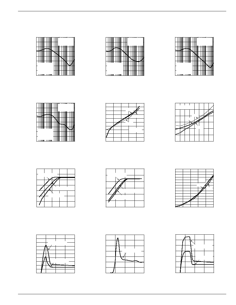
Typical Characteristics
0
20
40
60
80
1E+1 1E+2 1E+3 1E+4 1E+5 1E+6
PSRR (dB)
FREQUENCY (Hz)
Power Supply
Rejection Ratio
I
OUT
= 1A
C
OUT
= 10
µ
F
C
IN
= 0
V
IN
= 5V
V
OUT
= 3.3V
10
100
1k
10k
100k
1M
0
20
40
60
80
1E+1 1E+2 1E+3 1E+4 1E+5 1E+6
PSRR (dB)
FREQUENCY (Hz)
Power Supply
Rejection Ratio
I
OUT
= 1A
C
OUT
= 47
µ
F
C
IN
= 0
V
IN
= 5V
V
OUT
= 3.3V
10
100
1k
10k
100k
1M
0
20
40
60
80
1E+1 1E+2 1E+3 1E+4 1E+5 1E+6
PSRR (dB)
FREQUENCY (Hz)
Power Supply
Rejection Ratio
I
OUT
= 1A
C
OUT
= 10
µ
F
C
IN
= 0
V
IN
= 3.3V
V
OUT
= 2.5V
10
100
1k
10k
100k
1M
0
20
40
60
80
1E+1 1E+2 1E+3 1E+4 1E+5 1E+6
PSRR (dB)
FREQUENCY (Hz)
Power Supply
Rejection Ratio
I
OUT
= 1A
C
OUT
= 47
µ
F
C
IN
= 0
V
IN
= 3.3V
V
OUT
= 2.5V
10
100
1k
10k
100k
1M
0
50
100
150
200
250
300
350
400
450
500
0
250
500
750
1000 1250
DROPOUT VOLTAGE (mV)
OUTPUT CURRENT (mA)
Dropout Voltage
vs. Output Current
2.5V
3.3V
T
A
= 25
∞
C
1.8V
300
350
400
450
500
550
600
-40 -20 0
20 40 60 80 100 120
DROPOUT VOLTAGE (mV)
TEMPERATURE (
∞
C)
Dropout Voltage
vs. Temperature
3.3V
2.5V
I
LOAD
= 1A
1.8V
1.4
1.6
1.8
2.0
2.2
2.4
2.6
2.8
2
2.3
2.6
2.9
3.2
3.5
OUTPUT VOLTAGE (V)
SUPPLY VOLTAGE (V)
Dropout Characteristics
(2.5V)
ILOAD
=100mA
ILOAD
=750mA
ILOAD
=1A
2.4
2.6
2.8
3.0
3.2
3.4
3.6
2.8
3.2
3.6
4.0
4.4
OUTPUT VOLTAGE (V)
SUPPLY VOLTAGE (V)
Dropout Characteristics
(3.3V)
ILOAD
=100mA
ILOAD
=750mA
ILOAD
=1A
0
2
4
6
8
10
12
14
0
200
400
600
800
1000
GROUND CURRENT (mA)
OUTPUT CURRENT (mA)
Ground Current
vs. Output Current
2.5V
3.3V
1.8V
0
0.2
0.4
0.6
0.8
1.0
1.2
1.4
1.6
1.8
2.0
0
2
4
6
8
GROUND CURRENT (mA)
SUPPLY VOLTAGE (V)
Ground Current
vs. Supply Voltage (2.5V)
ILOAD
=
100mA
ILOAD
=
10mA
0
0.2
0.4
0.6
0.8
1.0
1.2
1.4
0
2
4
6
8
GROUND CURRENT (mA)
SUPPLY VOLTAGE (V)
Ground Current
vs. Supply Voltage (3.3V)
ILOAD
=100mA
ILOAD
=10mA
0
5
10
15
20
25
30
35
0
2
4
6
8
GROUND CURRENT (mA)
SUPPLY VOLTAGE (V)
Ground Current
vs. Supply Voltage (2.5V)
ILOAD
=1A