
1
SY100E310L
Micrel, Inc.
M9999-032206
hbwhelp@micrel.com or (408) 955-1690
DESCRIPTION
s
Guaranteed AC performance over temperature and
voltage:
∑ > 800MHz f
MAX
(typical)
∑ < 50ps within-device skew
s
Low voltage operation:
∑ LVPECL: +3.3V
±
10%
∑ LVECL: ≠3.3V
±
10%
s
Internal 75k
pull-down resistors
s
Guaranteed over industrial temperature range:
≠40
∞
C to +85
∞
C
s
Pin-for-pin, plug-in replacement for MC100LVE310
s
Available in 28-pin PLCC package
FEATURES
3.3V ECL/PECL
2:8 DIFFERENTIAL FANOUT BUFFER
SY100E310L
APPLICATIONS
s
Communications clock distribution
s
Redundant clock switchover
s
High-end server clock distribution
Rev.: D
Amendment: /0
Issue Date:
March 2006
The SY100E310L is a 3.3V, precision 2:8 ECL/PECL
fanout buffer optimized for precision low-skew clock
distribution. The SY100E310L features fully differential clock
paths to minimize both device and system skew resulting in
skew performance of < 50ps. In addition, the device includes
a 2:1 multiplexer input for redundant switchover applications.
The SY100E310L is optimized for low voltage +3.3V
LVPECL or ≠3.3V LVECL applications.
Data sheets and support documentation can be found on
Micrel's web site at www.micrel.com.
FUNCTIONAL BLOCK DIAGRAM
Micrel Semiconductor
On Semiconductor
SY100E310LJI
MC100LVE310FN
SY100E310LJITR
MC100LVE310FNR2
CROSS REFERENCE TABLE
CLKA
/CLKA
/CLKB
SEL
CLKB
Q0
/Q0
Q1
/Q1
Q2
/Q2
Q3
/Q3
Q4
/Q4
Q5
/Q5
Q6
/Q6
Q7
/Q7
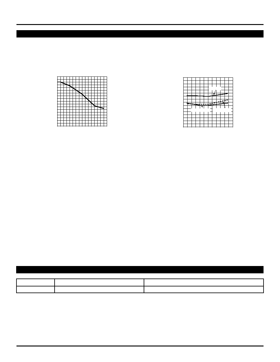
V
BB
0
100
200
300
400
500
600
700
800
900
0
200
400
600
800
1000
1200
1400
1600
Q AMPLITUDE (mV)
CLK FREQUENCY (MHz)
Output Swing
vs. Frequency
TYPICAL PERFORMANCE

2
SY100E310L
Micrel, Inc.
M9999-032206
hbwhelp@micrel.com or (408) 955-1690
PACKAGE/ORDERING INFORMATION
Pin Number
Pin Name
Pin Function
1
VCC
Positive Core Power Supply. Bypass with 0.1
µ
F
||
0.01
µ
F low ESR capacitors.
Not internally connected to V
CCO
. Must be externally connected to V
CCO
on PCB.
28, 2, 4, 5
CLKA, /CLKA
Differential Inputs: These input pairs are the differential data inputs to the device.
CLKB, /CLKB
3
VBB
Reference Voltage Output. Used for AC-coupled inputs or single-ended inputs.
6
NC
No Connect.
8, 15, 22
VCCO
Positive Power Supply. Bypass with 0.1
µ
F
||
0.01
µ
F low ESR capacitors.
Not internally connected to V
CC
. Must be externally connected to V
CC
on PCB.
24, 21, 19,
/Q0, /Q1, /Q2, /Q3
Differential Outputs.
17, 14, 12, 10, 7
/Q4, /Q5, /Q6, /Q7
25, 23, 20, 18,
Q0, Q1, Q2, Q3
Differential Outputs.
16, 13, 11, 9,
Q4, Q5, Q6, Q7
26
VEE
Negative Supply.
27
CLK_SEL
Single-Ended Clock Select.
PIN DESCRIPTION
/CLKB
NC
/Q7
VCCO
Q7
/Q6
Q6
Q0
/Q0
Q1
VCCO
/Q1
Q2
/Q2
4
5
6
7
8
9
10
11
25
24
23
22
21
20
19
3 2 1 28 27 26
12 13 14 15 16 17 18
Q4
VCCO
/Q4
Q5
/Q5
CLKA
VCC
/CLKA
VBB
CLKB
/Q3
Q3
CLK_SEL
VEE
28-Pin PLCC (J28-1)
Ordering Information
(1)
Package
Operating
Package
Lead
Part Number
Type
Range
Marking
Finish
SY100E310JI
J28-1
Industrial
SY100E310LJI
Sn-Pb
SY100E310JITR
(2)
J28-1
Industrial
SY100E310LJI
Sn-Pb
SY100E310JY
(3)
J28-1
Industrial
SY100E310JY with
Matte-Sn
Pb-Free bar-line indicator
SY100E310JYTR
(2, 3)
J28-1
Industrial
SY100E310JY with
Matte-Sn
Pb-Free bar-line indicator
Notes:
1. Contact factory for die availability. Dice are guaranteed at T
A
= 25
∞
C, DC Electricals only.
2. Tape and Reel.
3. Pb-Free package is recommended for new designs.

3
SY100E310L
Micrel, Inc.
M9999-032206
hbwhelp@micrel.com or (408) 955-1690
Absolute Maximum Ratings
(1)
Supply Voltage (V
CC
) ................................. ≠0.5V to +4.0V
Input Voltage (V
IN
) ........................................ ≠0.5V to V
CC
Termination Current
(3)
Source or sink current on V
BB
(I
BB
) .....................
±
0.5mA
Input Current
Source or sink current
(CLKA, /CLKA, CLKB, /CLKB, CLK_SEL) .........
±
50mA
Lead Temperature (soldering, 20 sec.) ................... +260
∞
C
Storage Temperature (T
S
) ...................... ≠65
∞
C to +150
∞
C
Operating Ratings
(2)
Supply Voltage (V
CC
) ................................. +3.0V to +3.6V
Ambient Temperature (T
A
) ........................ ≠40
∞
C to +85
∞
C
Package Thermal Resistance
PLCC
(
JA
)
Still-Air ......................................................... 63.5
∞
C/W
500lfpm ........................................................ 43.5
∞
C/W
T
A
= ≠40
∞
C to +85
∞
C; unless noted.
Symbol
Parameter
Condition
Min
Typ
Max
Units
V
CC
Power Supply
3.0
3.3
3.6
V
DC ELECTRICAL CHARACTERISTICS
(4)
V
CC
= +3.3V, V
EE
= 0V; T
A
= ≠40
∞
C to +85
∞
C; unless noted.
Symbol
Parameter
Condition
Min
Typ
Max
Units
I
CC
Power Supply Current
No load, max. V
CC
55
70
mA
V
OH
Output High Voltage
R
L
= 50
to V
CC
≠2V
2215
2345
2420
mV
(Q0-Q7, /Q0-/Q7)
V
OL
Output Low Voltage
R
L
= 50
to V
CC
≠2V
1470
1595
1680
mV
(Q0-Q7, /Q0-/Q7)
V
IH
Input High Voltage
2135
2420
mV
(CLKA, /CLKA, CLKB, /CLKB, CLK_SEL)
V
IL
Input Low Voltage
1490
1825
mV
(CLKA, /CLKA, CLKB, /CLKB, CLK_SEL)
V
IHCMR
Input High Voltage Common
Note 6
1.8
2.9
V
Mode Range (Differential)
(CLKA, / CLKA, CLKB, /CLKB)
V
BB
Output Reference Voltage
1.92
2.04
V
I
IN
Input HIGH Current
150
µ
A
(CLKA, /CLKA, CLKB,/CLKB, CLK_SEL)
I
IL
Input LOW Current
0.5
µ
A
(CLKA, /CLKA, CLKB, /CLKB, CLK_SEL)
Notes:
1. Permanent device damage may occur if Absolute Maximum Ratings are exceeded. This is a stress rating only and functional operation is not implied
at conditions other than those detailed in the operational sections of this data sheet. Exposure to Absolute Maximum Ratlng conditions for extended
periods may affect device reliability.
2. The data sheet limits are not guaranteed if the device is operated beyond the operating ratings.
3. Due to the limited drive capability use for input of the same package only.
4. The circuit is designed to meet the DC specifications shown in the above table after thermal equilibrium has been established.
5. Input and output parameters vary 1:1 with V
CC
. V
CC
can vary
±
0.3V.
6. V
IHCMR
is defined as the range within which the V
IH
level may vary with the device still meeting the propagation delay specification. The V
IL
level
must be such that the peak-to-peak voltage is less than 1.0V and then greater than or equal to V
PP
(min).
LVPECL DC ELECTRICAL CHARACTERISTICS
(4, 5)

4
SY100E310L
Micrel, Inc.
M9999-032206
hbwhelp@micrel.com or (408) 955-1690
V
CC
= +3.3V, V
EE
= 0V; T
A
= ≠40
∞
C to +85
∞
C; unless noted.
Symbol
Parameter
Condition
Min
Typ
Max
Units
V
OH
Output High Voltage
R
L
= 50
to V
CC
≠2V
≠1085
≠955
≠880
mV
(Q0-Q7, /Q0-/Q7)
V
OL
Output Low Voltage
R
L
= 50
to V
CC
≠2V
≠1830
≠1705
≠1620
mV
(Q0-Q7, /Q0-/Q7)
V
IH
Input High Voltage
≠1165
≠880
mV
(CLKA, /CLKA, CLKB, /CLKB, CLK_SEL)
V
IL
Input Low Voltage
≠1810
≠1475
mV
(CLKA, /CLKA, CLKB, /CLKB, CLK_SEL)
V
IHCMR
Input High Voltage Common
Note 9
≠1.5
≠0.4
V
Mode Range (Differential)
(CLKA, / CLKA, CLKB, /CLKB)
V
BB
Output Reference Voltage
≠1.38
≠1.26
V
I
IN
Input HIGH Current
150
µ
A
(CLKA, /CLKA, CLKB,/CLKB, CLK_SEL)
I
IL
Input LOW Current
0.5
µ
A
(CLKA, /CLKA, CLKB, /CLKB, CLK_SEL)
LVNECL DC ELECTRICAL CHARACTERISTICS
(7, 8)
V
CC
= +3.0 to +3.6V and V
EE
= 0V or V
CC
= 0V and V
EE
= ≠3.0 to ≠3.6V; T
A
= ≠40
∞
C to +85
∞
C; unless noted.
Symbol
Parameter
Condition
Min
Typ
Max
Units
f
MAX
Maximum Operating Frequency
V
OUT
= 400mV
800
MHz
t
PD
Propagation Delay
Note 10
525
725
ps
CLKA-to-Q, CLKB-to-Q (Differential)
CLKA-to-Q, CLKB-to-Q (Single-ended)
Note 11
500
750
ps
t
SKEW
Within-Device Skew
Note 12
50
ps
Part-to-Part Skew (Differential)
200
ps
t
JITTER
Cycle-to-Cycle Jitter
1
ps
RMS
V
PP
Input Swing
Note 13
500
1000
mV
t
r
, t
f
Rise / Fall Time (20% to 80%)
160
375
600
ps
(Q0-Q7, /Q0-/Q7)
Notes:
7. The circuit is designed to meet the DC specifications shown in the above table after thermal equilibrium has been established.
8. Input and output parameters vary 1:1 with V
CC
. V
CC
can vary
±
0.3V.
9. V
IHCMR
is defined as the range within which the V
IH
level may vary with the device still meeting the propagation delay specification. The V
IL
level
must be such that the peak-to-peak voltage is less than 1.0V and then greater than or equal to V
PP
(min).
10. The differential propagation delay is defined as the delay from the crossing points of the differential input signals to the crossing point of the
differential output signals.
11. The single-ended propagation delay is defined as the delay from the 50% point of the input signal to the 50% point of the output signal.
12. The within-device skew is defined as the worst case difference between any two similar delay paths within a single device.
13. V
PP
(min) is defined as the minimum input differential voltage which will cause no increase in the propagation delay. The V
PP
(min) is AC limited for
the E310L as a differential input as low as 50 mV will still produce full ECL levels at the output.
AC ELECTRICAL CHARACTERISTICS
5
SY100E310L
Micrel, Inc.
M9999-032206
hbwhelp@micrel.com or (408) 955-1690
Part Number
Function
Data Sheet Link
HBW Solutions
New Products and Applications
www.micrel.com/product-info/products/solutions.shtml
RELATED PRODUCT AND SUPPORT DOCUMENTATION
TYPICAL OPERATING CHARACTERISTICS
V
CC
= 3.3V, T
A
= 25
∞
C
0
100
200
300
400
500
600
700
800
900
0
200
400
600
800
1000
1200
1400
1600
Q AMPLITUDE (mV)
CLK FREQUENCY (MHz)
Output Swing
vs. Frequency
500
525
550
575
600
625
650
675
700
-50
-25
0
25
50
75
100
PROPAGATION DELAY (ps)
TEMPERATURE (
∞
C) (Forced Air)
Input to Q
Propagation Delay
vs. Temperature
CLK-Q(Diff)
SEL-Q
CLK-Q(S-E)