FEATURES
s
1500ps max. clock to bus (data transmit)
s
1000ps max. clock to Q (data receive)
s
Extended 100E V
EE
range of ≠4.2V to ≠5.5V
s
25
cutoff bus outputs
s
50
receiver outputs
s
Scannable implementation of E336
s
Synchronous and asynchronous bus enables
s
Non-inverting data path
s
Bus outputs feature internal edge slow-down
capacitors
s
Additional package ground pins
s
Fully compatible with industry standard 10KH,
100K ECL levels
s
Internal 75K
input pulldown resistors
s
Fully compatible with Motorola MC10E/100E337
s
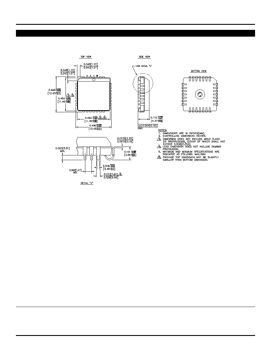
Available in 28-pin PLCC package
3-BIT SCANNABLE
REGISTERED BUS
TRANSCEIVER
DESCRIPTION
The SY10/100E337 are 3-bit registered bus transceivers
with scan designed for use in new, high- performance ECL
systems. The bus outputs (BUS
0
≠BUS
2
) are designed to
drive a 25
bus; the receive outputs (Q
0
≠Q
2
) are designed
for 50
. The bus outputs feature a normal logic HIGH level
(V
OH
) and a cutoff LOW level of ≠2.0V and the output
emitter-follower is "off", presenting a high impedance to the
bus. The bus outputs also feature edge slow-down
capacitors.
Both drive and receive sides feature the same logic,
including a loopback path to hold data. The LOAD/HOLD
function is controlled by Transmit Enable (TEN) and Receive
Enable (REN) on the transmit and receive sides,
respectively, with a HIGH selecting LOAD. The
implementation of the E337 Receive Enable differs from
that of the E336.
A synchronous bus enable (SBUSEN) is provided for
normal, non-scan operation. The asynchronous bus disable
(ABUSDIS) disables the bus for scan mode.
The SYNCEN input allows either synchronous or
asynchronous re-enabling after disabling with ABUSDIS.
An alternative use is asynchronous-only operation with
ABUSDIS, in which case SYNCEN is tied LOW. SYNCEN
is implemented as an overriding SET control to the enable
flip-flop.
Scan mode is selected by a logic HIGH at the SCAN
input. Scan input data is shifted in through S-IN, and output
data appears at the Q
2
output.
All registers are clocked on the rising edge of CLK.
Additional lead-frame grounding is provided through the
ground pins (GND) which should be connected to 0V. The
GND pins are not electrically connected to the chip.
SY10E337
SY100E337
Rev.: C
Amendment: /2
Issue Date:
February, 1998
Pin
Function
A
0
≠A
2
Data Inputs A
B
0
≠B
2
Data Inputs B
S-IN
Serial (Scan) Data Input
TEN, REN
LOAD/HOLD Controls
SCAN
Scan Control
ABUSDIS
Asynchronous Bus Disable
SBUSEN
Synchronous Bus Enable
SYNCEN
Synchronous Enable Control
CLK
Clock
BUS
0
≠BUS
2
25
Cutoff BUS Outputs
Q
0
≠Q
2
Receive Data Outputs (Q
2
serves as
SCAN_OUT in scan mode)
V
CCO
V
CC
to Output
PIN NAMES
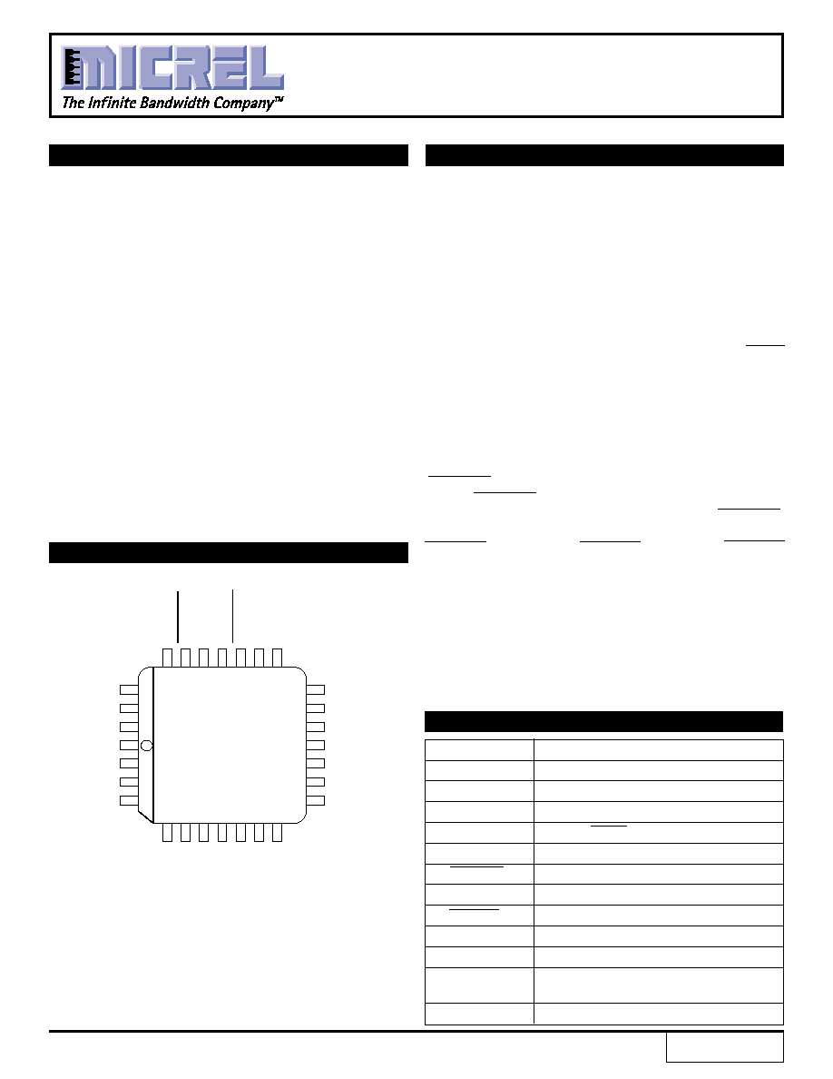
PIN CONFIGURATION
TOP VIEW
PLCC
J28-1
26
27
28
1
2
3
4
18
17
16
15
14
13
12
25 24 23 22 21 20 19
5
6
7
8
9
10 11
V
CC
GND
BUS
0
GND
Q
1
BUS
1
V
CCO
V
EE
A
1
TEN
CLK
REN
SCAN
S-IN
B
2
V
CCO
Q
2
A
2
B
1
BUS
2
GND
V
CCO
A
0
B
0
SBUSEN
Q
0
SYNCEN
ABUSDIS
1