Pin
Function
SIN, SIN
Differential Serial Data Input
D
0
≠ D
3
Parallel Data Input
SOUT, SOUT
Differential Serial Data Output
CLK, CLK
Differential Clock Input
CL/4, CL/4
Differential 4 Clock Output
CL/8, CL/8
Differential 8 Clock Output
MODE
Conversion Mode, 4-bit/8-bit
SYNC
Conversion Synchronizing Input
V
CCO
V
CC
to Output
DESCRIPTION
FEATURES
s
On-chip clock
˜
4 and
˜
8
s
Extended 100E V
EE
range of ≠4.2V to ≠5.5V
s
1.6Gb/s typical data rate capability
s
Differential clock and serial inputs
s
VBB output for single-ended use
s
Asynchronous data synchronization
s
Mode select to expand to 8 bits
s
Internal 75K
input pulldown resistors
s
Fully compatible with Motorola MC10E/100E446
s
Available in 28-pin PLCC package
4-BIT PARALLEL-TO-SERIAL
CONVERTER
The SY10/100E446 are integrated 4-bit parallel-to-
serial data converters. These devices are designed to
operate for NRZ data rates of up to a minimum of 1.3Gb/
s. The chips generate a divide-by-4 and a divide-by-8
clock for both 4-bit conversion and a two-chip 8-bit
conversion function. The conversion sequence was
chosen to convert the parallel data into a serial stream
from bit D
0
to D
3
. A serial input is provided to cascade
two E446 devices for 8-bit conversion applications.
The SYNC input will asynchronously reset the internal
clock circuitry. This pin allows the user to reset the internal
clock conversion unit and, thus, select the start of the
conversion process.
The MODE input is used to select the conversion mode
of the device. With the MODE input LOW (or open) the
device will function as a 4-bit converter. When the mode
input is driven HIGH, the internal load clock will change
on every eighth clock cycle, thus allowing for an 8-bit
conversion scheme using two E446s. When cascaded in
an 8-bit conversion scheme, the devices will not operate
at the 1.3Gb/s data rate of a single device. Refer to the
applications section of this data sheet for more information
on cascading the E446.
For lower data rate applications, a V
BB
reference
voltage is supplied for single-ended inputs. When
operating at clock rates above 500MHz, differential input
signals are recommended. For single-ended inputs, the
V
BB
pin is tied to the inverting differential input and
bypassed via a 0.01
µ
F capacitor. The V
BB
provides the
switching reference for the input differential amplifier. The
V
BB
can also be used to AC couple an input signal.
Rev.: C
Amendment: /1
Issue Date:
February, 1998
SY10E446
SY100E446
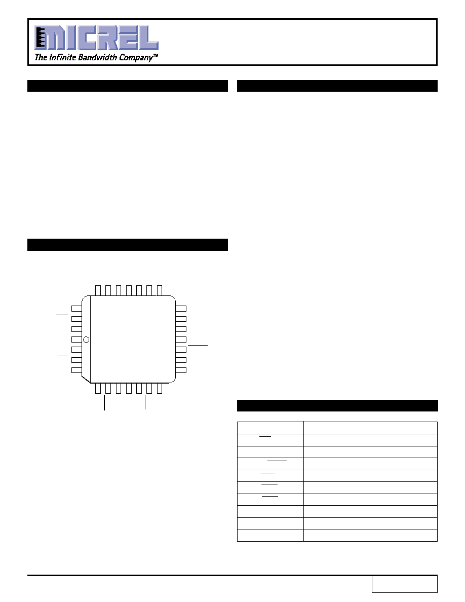
PIN CONFIGURATION
18
17
16
15
14
13
12
5
6
7
8
9
10 11
26
27
28
1
2
3
4
TOP VIEW
PLCC
J28-1
25 24 23 22 21 20 19
D
2
D
3
MODE
NC
D
0
D
1
NC
CLK
V
BB
V
EE
SIN
SYNC
CLK
SIN
V
CCO
CL/8
V
CCO
CL/4
V
CCO
CL/8
CL/4
NC
NC
V
CC
SOUT
V
CCO
NC
SOUT
PIN NAMES
1

3
SY10E446
SY100E446
Micrel
T
A
= 0
∞
C
T
A
= +25
∞
C
T
A
= +85
∞
C
Symbol
Parameter
Min.
Typ.
Max. Min.
Typ.
Max.
Min.
Typ.
Max.
Unit
Condition
f
MAX
Max. Conversion Frequency
1.3
1.6
--
1.3
1.6
--
1.3
1.6
--
Gb/s
--
NRZ
t
PLH
Propagation Delay to Output
ps
--
t
PHL
CLK to SOUT
1000
1400
1700 1000
1400
1700
1000
1400
1700
CLK to CL/4
500
800
1100
500
800
1100
500
800
1100
CLK to CL/8
800
1100
1400
800
1100
1400
800
1100
1400
SYNC to CL/4, CL/8
500
800
1100
500
800
1100
500
800
1100
t
S
Set-up Time
ps
--
SIN
≠200
≠400
--
≠200
≠400
--
≠200
≠400
--
D
n
≠200
≠400
--
≠200
≠400
--
≠200
≠400
--
Mode
0
≠250
--
0
≠250
--
0
≠250
--
t
H
Hold Time
ps
--
SIN
750
550
--
750
550
--
750
550
--
D
n
800
600
--
800
600
--
800
600
--
Mode
500
300
--
500
300
--
500
300
--
t
RR
Reset Recovery Time
500
200
--
500
200
--
500
200
--
ps
--
t
PW
Minimum Pulse Width
400
--
--
400
--
--
400
--
--
ps
--
CLK, MR
t
r
Rise/Fall Time
ps
20≠80%
t
f
SOUT
100
225
350
100
225
350
100
225
350
Other
200
425
650
200
425
650
200
425
650
AC ELECTRICAL CHARACTERISTICS
V
EE
= V
EE
(Min.) to V
EE
(Max.); V
CC
= V
CCO
= GND
DC ELECTRICAL CHARACTERISTICS
V
EE
= V
EE
(Min.) to V
EE
(Max.); V
CC
= V
CCO
= GND
T
A
= 0
∞
C
T
A
= +25
∞
C
T
A
= +85
∞
C
Symbol
Parameter
Min.
Typ.
Max.
Min.
Typ.
Max.
Min.
Typ.
Max.
Unit
Condition
I
IH
Input HIGH Current
--
--
150
--
--
150
--
--
150
µ
A
--
V
OH
Output HIGH Voltage
V
1
(SOUT Only) 10E
≠1020
--
≠790
≠980
--
≠760
≠910
--
≠670
(SOUT Only) 100E
≠1025
--
≠830 ≠1025
--
≠830 ≠1025
--
≠830
V
BB
Output Reference Voltage
V
--
10E
≠1.38
--
≠1.27 ≠1.35
--
≠1.25 ≠1.31
--
≠1.19
100E
≠1.38
--
≠1.26 ≠1.38
--
≠1.26 ≠1.38
--
≠1.26
I
EE
Power Supply Current
mA
--
10E
--
110
132
--
110
132
--
110
132
100E
--
110
132
--
110
132
--
127
152
NOTE:
1. The maximum V
OH
limit was relaxed from standard ECL due to the high frequency output design. All other outputs are specified with the standard 10E
and 100E V
OH
levels.
TRUTH TABLE
Mode
Conversion
L
4-Bit
H
8-Bit


