
The SY10/100EL15 are low skew 1:4 clock distribution
chips designed explicitly for low skew clock distribution
applications. The device can be driven by either a
differential or single-ended ECL or, if positive power
supplies are used, PECL input signal. If a single-ended
input is to be used the V
BB
output should be connected
to the CLK input and bypassed to V
CC
via a 0.01
µ
F
capacitor. The V
BB
output is designed to act as the
switching reference for the input of the EL15 under single-
ended input conditions, as a result this pin can only
source/sink up to 0.5mA of current.
The EL15 features a multiplexed clock input to allow
for the distribution of a lower speed scan or test clock
along with the high speed system clock. When LOW (or
left open and pulled LOW by the input pull-down resistor)
the SEL pin will select the differential clock input.
The common enable (EN) is synchronous so that the
outputs will only be enabled/disabled when they are
already in the LOW state. This avoids any chance of
generating a runt clock pulse when the device is enabled/
disabled as can happen with an asynchronous control.
The internal flip flop is clocked on the falling edge of the
input clock, therefore all associated specification limits
are referenced to the negative edge of the clock input.
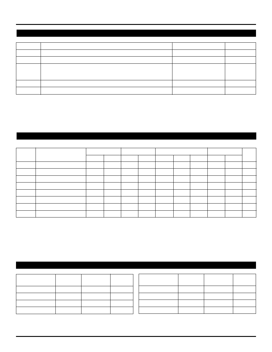
Pin
Function
CLK
Differential Clock Inputs
SCLK
Synchronous Clock Input
EN
Synchronous Enable
SEL
Clock Select Input
V
BB
Reference Output
Q
0-3
Differential Clock Outputs
TRUTH TABLE
PIN NAMES
FEATURES
DESCRIPTION
PIN CONFIGURATION/BLOCK DIAGRAM
Precision EdgeTM
SY10EL15
SY100EL15
FINAL
CLK
SCLK
SEL
EN
Q
L
X
L
L
L
H
X
L
L
H
X
L
H
L
L
X
H
H
L
H
X
X
X
H
L*
* On next negative transition of CLK or SCLK
V
CC
CLK
Q
0
Q
0
Q
1
Q
2
Q
2
Q
3
Q
3
V
EE
SEL
V
BB
CLK
EN
16
15
14
13
12
11
10
9
Q
1
1
2
3
4
5
6
7
8
D
Q
1 0
SCLK
SOIC
TOP VIEW
s
50ps output-to-output skew
s
Synchronous enable/disable
s
Multiplexed clock input
s
75K
internal input pull-down resistors
s
Available in 16-pin SOIC package
1:4 CLOCK
DISTRIBUTION
1
Rev.: G
Amendment: /0
Issue Date:
February 2003
Precision Edge is a trademark of Micrel, Inc.
Precision EdgeTM
2
Precision EdgeTM
SY10EL15
SY100EL15
Micrel
Symbol
Rating
Value
Unit
V
EE
Power Supply (V
CC
= 0V)
≠8.0 to 0
VDC
V
I
Input Voltage (V
CC
= 0V)
0 to ≠6.0
VDC
I
OUT
Output Current
≠Continuous
50
mA
≠Surge
100
T
A
Operating Temperature Range
≠40 to +85
∞
C
V
EE
Operating Range
(1),(2)
≠5.7 to ≠4.2
V
NOTES:
1. Absolute maximum rating, beyond which, device life may be impaired, unless otherwise specified on an individual data sheet.
2. Parametric values specified at:
100EL15 Series:
≠4.2V to ≠5.5V.
10EL15 Series
≠4.75V to ≠5.5V.
ABSOLUTE MAXIMUM RATINGS
(1)
NOTE:
1. 10EL circuits are designed to meet the DC specifications shown in the table after thermal equilibrium has been established. The circuit is in a test socket
or mounted on a printed circuit board and transverse airflow greater than 500lfpm is maintained. Outputs are terminated through a 50
resistor to ≠2.0V
except where otherwise specified on the individual data sheets.
T
A
= ≠40
∞
C
T
A
= 0
∞
C
T
A
= +25
∞
C
T
A
= +85
∞
C
Symbol
Parameter
Min.
Max.
Min.
Max.
Min.
Typ.
Max.
Min.
Max.
Unit
V
OH
Output HIGH Voltage
≠1080
≠890
≠1020
≠840
≠980
--
≠810
≠910
≠720
mV
V
OL
Output LOW Voltage
≠1950
≠1650
≠1950
≠1630
≠1950
--
≠1630
≠1950
≠1595
mV
V
IH
Input HIGH Voltage
≠1230
≠890
≠1170
≠840
≠1130
--
≠810
≠1060
≠720
mV
V
IL
Input LOW Voltage
≠1950
≠1500
≠1950
≠1480
≠1950
--
≠1480
≠1950
≠1445
mV
I
IH
Input High Current
--
150
--
150
--
--
150
--
150
µ
A
I
IL
Input LOW Current
0.5
--
0.5
--
0.5
--
--
0.5
--
µ
A
I
EE
Power Supply Current
--
35
--
35
--
25
35
--
38
mA
V
BB
Output Reference Voltage
≠1.38
≠1.26
≠1.38
≠1.26
≠1.38
--
≠1.26
≠1.38
≠1.26
V
10EL DC ELECTRICAL CHARACTERISTICS
V
EE
= V
EE
(Min.) to V
EE
(Max.); V
CC
= GND
(1)
PRODUCT ORDERING CODE
Ordering
Package
Operating
Marking
Code
Type
Range
Code
SY10EL15ZC
Z16-2
Commercial
HEL15
SY10EL15ZCTR*
Z16-2
Commercial
HEL15
SY100EL15ZC
Z16-2
Commercial
XEL15
SY100EL15ZCTR*
Z16-2
Commercial
XEL15
*Tape and Reel
Note 1.
Recommended for new designs.
Ordering
Package
Operating
Marking
Code
Type
Range
Code
SY10EL15ZI
(1)
Z16-2
Industrial
HEL15
SY10EL15ZITR*
(1)
Z16-2
Industrial
HEL15
SY100EL15ZI
(1)
Z16-2
Industrial
XEL15
SY100EL15ZITR*
(1)
Z16-2
Industrial
XEL15
*Tape and Reel
3
Precision EdgeTM
SY10EL15
SY100EL15
Micrel
T
A
= ≠40
∞
C
T
A
= 0
∞
C
T
A
= +25
∞
C
T
A
= +85
∞
C
Symbol
Parameter
Min.
Max.
Min.
Max.
Min.
Typ.
Max.
Min.
Max.
Unit
V
OH
Output HIGH Voltage
(2)
≠1085
≠880
≠1025
≠880
≠1025
≠955
≠880
≠1025
≠880
mV
V
OL
Output LOW Voltage
(2)
≠1830
≠1555
≠1810
≠1620
≠1810
≠1705
≠1620
≠1810
≠1620
mV
V
OHA
Output HIGH Voltage
(3)
≠1095
--
≠1035
--
≠1035
--
--
≠1035
--
mV
V
OLA
Output LOW Voltage
(3)
--
≠1555
--
≠1610
--
--
≠1610
--
≠1610
mV
V
IH
Input HIGH Voltage
≠1165
≠880
≠1165
≠880
≠1165
--
≠880
≠1165
≠880
mV
V
IL
Input LOW Voltage
≠1810
≠1475
≠1810
≠1475
≠1810
--
≠1475
≠1810
≠1475
mV
I
IH
Input High Current
--
150
--
150
--
--
150
--
150
µ
A
I
IL
Input LOW Current
(4)
0.5
--
0.5
--
0.5
--
--
0.5
--
µ
A
I
EE
Power Supply Current
--
35
--
35
--
25
35
--
38
mA
V
BB
Output Reference Voltage
≠1.38
≠1.26
≠1.38
≠1.26
≠1.38
--
≠1.26
≠1.38
≠1.26
V
100EL DC ELECTRICAL CHARACTERISTICS
V
EE
= V
EE
(Min.) to V
EE
(Max.); V
CC
= GND
(1)
NOTES:
1. This table replaces the three traditionally seen in ECL 100K data books. The same DC parameter values at V
EE
= ≠4.5V now apply across the full V
EE
range of ≠4.2V to ≠5.5V. Outputs are terminated through a 50
resistor to ≠2.0V except where otherwise specified on the individual data sheets.
2. V
IN
= V
IH
(Max) or V
IL
(Min).
3. V
IN
= V
IH
(Min) or V
IL
(Max).
4. V
IN
= V
IL
(Max).
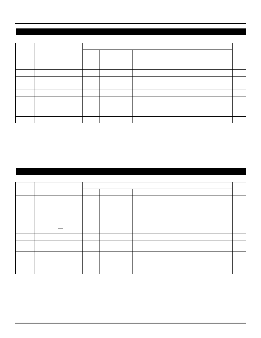
T
A
= ≠40
∞
C
T
A
= 0
∞
C
T
A
= +25
∞
C
T
A
= +85
∞
C
Symbol
Parameter
Min.
Max.
Min.
Max.
Min.
Typ.
Max.
Min.
Max.
Unit
t
PLH
Propagation Delay
ps
t
PHL
CLK to Q (Diff)
460
660
470
670
470
--
670
500
700
CLK to Q (SE)
410
710
420
720
420
--
720
450
750
SCLK to Q
410
710
420
720
420
--
720
470
750
t
skew
Part-to-Part Skew
(1)
--
200
--
200
--
--
200
--
200
ps
Within-Device Skew
--
50
--
50
--
--
50
--
50
t
S
Setup Time EN
150
--
150
--
150
--
--
150
--
ps
t
H
Hold Time EN
400
--
400
--
400
--
--
400
--
ps
V
PP
Minimum Input
CLK
250
--
250
--
250
--
--
250
--
mV
Swing
V
CMR
Common Mode
CLK
≠2.0
≠0.4
≠2.0
≠0.4
≠2.0
--
≠0.4
≠2.0
≠0.4
V
Range
t
r
Output Rise/Fall Times Q
--
--
325
575
325
--
575
325
575
ps
t
f
(20% ≠ 80%)
AC ELECTRICAL CHARACTERISTICS
V
EE
= V
EE
(Min) to V
EE
(Max); V
CC
= GND
NOTE:
1. Skews are specified for identical LOW-to-HIGH or HIGH-to-LOW
transitions.

4
Precision EdgeTM
SY10EL15
SY100EL15
Micrel
16 LEAD SOIC .150" WIDE (Z16-2)
Rev. 02
MICREL, INC.
1849 FORTUNE DRIVE
SAN JOSE, CA 95131
USA
TEL
+ 1 (408) 944-0800
FAX
+ 1 (408) 944-0970
WEB
http://www.micrel.com
The information furnished by Micrel in this datasheet is believed to be accurate and reliable. However, no responsibility is assumed by Micrel for its use.
Micrel reserves the right to change circuitry and specifications at any time without notification to the customer.
Micrel Products are not designed or authorized for use as components in life support appliances, devices or systems where malfunction of a product can
reasonably be expected to result in personal injury. Life support devices or systems are devices or systems that (a) are intended for surgical implant into
the body or (b) support or sustain life, and whose failure to perform can be reasonably expected to result in a significant injury to the user. A Purchaser's
use or sale of Micrel Products for use in life support appliances, devices or systems is at Purchaser's own risk and Purchaser agrees to fully indemnify
Micrel for any damages resulting from such use or sale.
© 2003 Micrel, Incorporated.