
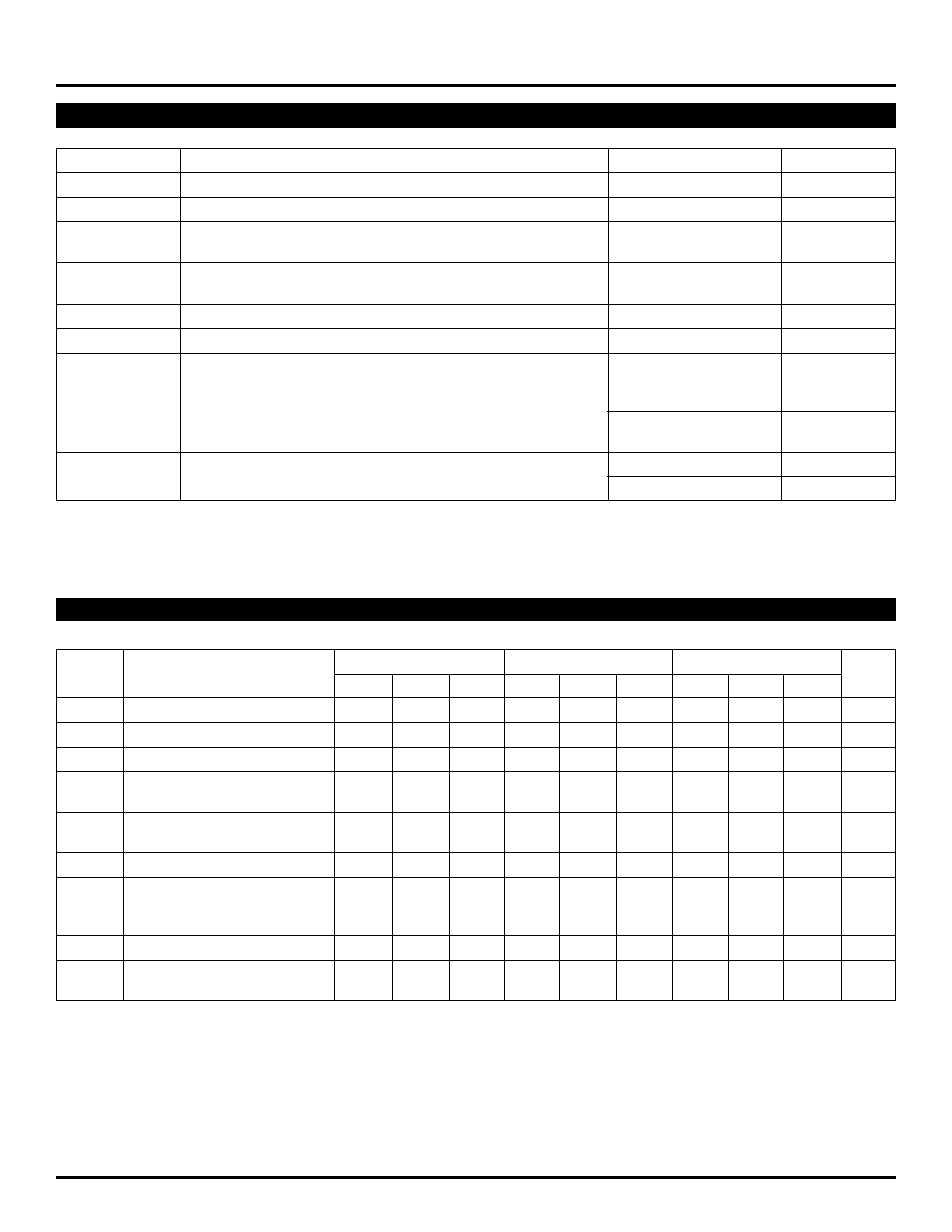
CLK
/CLK
RESET
Q
/Q
X
X
Z
L
H
L
F
F
1
DESCRIPTION
s
Guaranteed maximum frequency >4GHz
s
3.3V and 5V power supply options
s
Guaranteed propagation delay <460ps over
temperature
s
Wide operating temperature range: ≠40
∞
C to +85
∞
C
s
Available in 8-pin MSOP and SOIC packages
The SY10/100EP33V is an integrated
˜
4 divider.
The V
BB
pin, an internally generated voltage supply,
is available to this device only. For single-ended input
conditions, the unused differential input is connected to
V
BB
as a switching reference voltage. V
BB
may also rebias
AC-coupled inputs. When used, decouple V
BB
and V
CC
via a 0.01
µ
F capacitor and limit current sourcing or sinking
to 0.5mA. When not used, V
BB
should be left open.
The reset pin is asynchronous and is asserted on the
rising edge. Upon power-up, the internal flip-flops will
attain a random state; the reset allows for the
synchronous use of multiple EP33s in a system.
The 100K Series includes internal temperature
compensation circuitry.
FEATURES
PIN CONFIGURATION/BLOCK DIAGRAM
PIN NAMES
5V/3.3V 4GHz,
˜
4 PECL/LVPECL DIVIDER
1
2
3
4
5
6
7
8
RESET
VCC
Q
VEE
CLK
VBB
/Q
R
/CLK
˜ 4
TOP VIEW
(Available in MSOP or SOIC package)
Pin
Function
CLK, /CLK
ECL Clock Inputs with Internal 75k
Pull-Down Resistor, Default State is LOW
RESET
ECL Asynchronous Reset
V
BB
Reference Voltage Output
Q, /Q
ECL Data Outputs
Rev.: C
Amendment: /0
Issue Date:
March 2003
Precision EdgeTM
SY10EP33V
SY100EP33V
FINAL
TRUTH TABLE
(1)
Note 1.
F = Divide by 4 function
ECL ProTM
Precision Edge and ECL Pro are trademarks of Micrel, Inc.
2
Precision EdgeTM
SY10EP33V
SY100EP33V
Micrel
Symbol
Rating
Value
Unit
V
CC
Power Supply Voltage (V
EE
= 0)
+6.0 to 0
V
V
EE
Power Supply Voltage (V
CC
= 0)
≠6.0 to 0
V
V
IN
Input Voltage (V
CC
= 0V, V
IN
not more negative than V
EE
)
≠6.0 to 0
V
Input Voltage (V
EE
= 0V, V
IN
not more positive than V
CC
)
+6.0 to 0
V
I
OUT
Output Current
≠Continuous
50
mA
≠Surge
100
T
A
Operating Temperature Range
≠40 to +85
∞
C
T
store
Storage Temperature Range
≠65 to +150
∞
C
JA
Thermal Resistance (Junction-to-Ambient)
SOIC-8
≠Still Air
160
∞
C/W
≠500lfpm
109
∞
C/W
MSOP-8
≠Still Air
206
∞
C/W
≠500lfpm
155
∞
C/W
JC
Thermal Resistance (Junction-to-Case)
SOIC-8
39
∞
C/W
MSOP-8
39
∞
C/W
Note 1.
Permanent device damage may occur if ABSOLUTE MAXIMUM RATINGS are exceeded. This is a stress rating only and functional operation
is not implied at conditions other than those detailed in the operational sections of this data sheet. Exposure to ABSOLUTE MAXIMUM
RATlNG conditions for extended periods may affect device reliability.
ABSOLUTE MAXIMUM RATINGS
(1)
T
A
= ≠40
∞
C
T
A
= +25
∞
C
T
A
= +85
∞
C
Symbol
Parameter
Min.
Typ.
Max.
Min.
Typ.
Max.
Min.
Typ.
Max.
Unit
I
EE
Power Supply Current
--
--
36
--
26
36
--
--
36
mA
V
OH
Output HIGH Voltage
(3)
2165
2290
2415
2230
2355
2480
2290
2415
2540
mV
V
OL
Output LOW Voltage
(3)
1365
1490
1615
1430
1555
1680
1490
1615
1740
mV
V
IH
Input HIGH Voltage
2090
--
2415
2155
--
2480
2215
--
2540
mV
(Single-Ended)
V
IL
Input LOW Voltage
1365
--
1690
1430
--
1755
1490
--
1815
mV
(Single-Ended)
V
BB
Output Voltage
1790
1890
1990
1885
1955
2055
1915
2015
2115
mV
V
IHCMR
Input HIGH Voltage
(4)
Common Mode Range
2.0
--
V
CC
2.0
--
V
CC
2.0
--
V
CC
V
(Differential)
I
IH
Input HIGH Current
--
--
150
--
--
150
--
--
150
µ
A
I
IL
Input LOW
RESET, CLK
0.5
--
--
0.5
--
--
0.5
--
--
µ
A
Current
/CLK
≠150
--
--
≠150
--
--
≠150
--
--
Note 1.
10EP circuits are designed to meet the DC specifications shown in the above table after thermal equilibrium has been established. The circuit
is in a test socket or mounted on a printed circuit board and traverse airflow greater than 500lfpm is maintained.
Note 2.
Input and output parameters vary 1:1 with V
CC
.
Note 3.
All loading with 50
to V
CC
≠2.0V.
Note 4.
The V
IHCMR
range is referenced to the most positive side of the differential input signal.
(10EP) LVPECL DC ELECTRICAL CHARACTERISTICS
(1)
V
CC
= +3.3V
±
10%; V
EE
= 0V
(2)
3
Precision EdgeTM
SY10EP33V
SY100EP33V
Micrel
T
A
= ≠40
∞
C
T
A
= +25
∞
C
T
A
= +85
∞
C
Symbol
Parameter
Min.
Typ.
Max.
Min.
Typ.
Max.
Min.
Typ.
Max.
Unit
I
EE
Power Supply Current
--
--
36
--
26
36
--
--
36
mA
V
OH
Output HIGH Voltage
(3)
3865
3990
4115
3930
4055
4180
3990
4115
4240
mV
V
OL
Output LOW Voltage
(3)
3065
3190
3315
3130
3255
3380
3190
3315
3440
mV
V
IH
Input HIGH Voltage
3790
--
4115
3855
--
4180
3915
--
4240
mV
(Single-Ended)
V
IL
Input LOW Voltage
3065
--
3390
3130
--
3455
3190
--
3515
mV
(Single-Ended)
V
BB
Output Voltage
3490
3590
3690
3555
3655
3755
3615
3715
3815
mV
V
IHCMR
Input HIGH Voltage
(4)
Common Mode Range
2.0
--
V
CC
2.0
--
V
CC
2.0
--
V
CC
V
(Differential)
I
IH
Input HIGH Current
--
--
150
--
--
150
--
--
150
µ
A
I
IL
Input LOW
RESET, CLK
0.5
--
--
0.5
--
--
0.5
--
--
µ
A
Current
/CLK
≠150
--
--
≠150
--
--
≠150
--
--
Note 1.
10EP circuits are designed to meet the DC specifications shown in the above table after thermal equilibrium has been established. The circuit
is in a test socket or mounted on a printed circuit board and traverse airflow greater than 500lfpm is maintained.
Note 2.
Input and output parameters vary 1:1 with V
CC
.
Note 3.
All loading with 50
to V
CC
≠2.0V.
Note 4.
The V
IHCMR
range is referenced to the most positive side of the differential input signal.
(10EP) PECL DC ELECTRICAL CHARACTERISTICS
(1)
V
CC
= +5.0V
±
10%; V
EE
= 0V
(2)
T
A
= ≠40
∞
C
T
A
= +25
∞
C
T
A
= +85
∞
C
Symbol
Parameter
Min.
Typ.
Max.
Min.
Typ.
Max.
Min.
Typ.
Max.
Unit
I
EE
Power Supply Current
--
--
36
--
26
36
--
--
36
mA
V
OH
Output HIGH Voltage
(3)
≠1135
≠1010
≠885
≠1070
≠945
≠820
≠1010
≠885
≠760
mV
V
OL
Output LOW Voltage
(3)
≠1935
≠1810
≠1685
≠1870
≠1745
≠1620
≠1810
≠1685
≠1560
mV
V
IH
Input HIGH Voltage
≠1210
--
≠885
≠1145
--
≠820
≠1085
--
≠760
mV
(Single-Ended)
V
IL
Input LOW Voltage
≠1935
--
≠1610
≠1870
--
≠1545
≠1810
--
≠1485
mV
(Single-Ended)
V
BB
Output Voltage
≠1510
≠1410
≠1310
≠1445
≠1345
≠1245
≠1385
≠1285
≠1185
mV
V
IHCMR
Input HIGH Voltage
(4)
Common Mode Range
V
EE
+2.0
0.0
V
EE
+2.0
0.0
V
EE
+2.0
0.0
V
(Differential)
I
IH
Input HIGH Current
--
--
150
--
--
150
--
--
150
µ
A
I
IL
Input LOW
RESET, CLK
0.5
--
--
0.5
--
--
0.5
--
--
µ
A
Current
/CLK
≠150
--
--
≠150
--
--
≠150
--
--
Note 1.
10EP circuits are designed to meet the DC specifications shown in the above table after thermal equilibrium has been established. The circuit
is in a test socket or mounted on a printed circuit board and traverse airflow greater than 500lfpm is maintained.
Note 2.
Input and output parameters vary 1:1 with V
CC
.
Note 3.
All loading with 50
to V
CC
≠2.0V.
Note 4.
V
IHCMR
(Min) varies 1:1 with V
EE
. The V
IHCMR
range is referenced to the most positive side of the differential input signal.
(10EP) ECL/LVECL DC ELECTRICAL CHARACTERISTICS
(1)
V
CC
= 0V; V
EE
= ≠3.3V to ≠5.0V
±
10%
(2)

5-4
Precision EdgeTM
SY10EP33V
SY100EP33V
Micrel
T
A
= ≠40
∞
C
T
A
= +25
∞
C
T
A
= +85
∞
C
Symbol
Parameter
Min.
Typ.
Max.
Min.
Typ.
Max.
Min.
Typ.
Max.
Unit
I
EE
Power Supply Current
--
--
36
--
30
36
--
--
40
mA
V
OH
Output HIGH Voltage
(3)
2155
2280
2405
2155
2280
2405
2155
2280
2405
mV
V
OL
Output LOW Voltage
(3)
1355
1480
1605
1355
1480
1605
1355
1480
1605
mV
V
IH
Input HIGH Voltage
2075
--
2420
2075
--
2420
2075
--
2420
mV
(Single-Ended)
V
IL
Input LOW Voltage
1355
--
1675
1355
--
1675
1355
--
1675
mV
(Single-Ended)
V
BB
Output Voltage
1775
1875
1975
1775
1875
1975
1775
1875
1975
mV
V
IHCMR
Input HIGH Voltage
(4)
Common Mode Range
2.0
--
V
CC
2.0
--
V
CC
2.0
--
V
CC
V
(Differential)
I
IH
Input HIGH Current
--
--
150
--
--
150
--
--
150
µ
A
I
IL
Input LOW
RESET, CLK
0.5
--
--
0.5
--
--
0.5
--
--
µ
A
Current
/CLK
≠150
--
--
≠150
--
--
≠150
--
--
Note 1.
100EP circuits are designed to meet the DC specifications shown in the above table after thermal equilibrium has been established. The circuit
is in a test socket or mounted on a printed circuit board and traverse airflow greater than 500lfpm is maintained.
Note 2.
Input and output parameters vary 1:1 with V
CC
.
Note 3.
All loading with 50
to V
CC
≠2.0V.
Note 4.
The V
IHCMR
range is referenced to the most positive side of the differential input signal.
(100EP) LVPECL DC ELECTRICAL CHARACTERISTICS
(1)
V
CC
= +3.3V
±
10%; V
EE
= 0V
(2)
T
A
= ≠40
∞
C
T
A
= +25
∞
C
T
A
= +85
∞
C
Symbol
Parameter
Min.
Typ.
Max.
Min.
Typ.
Max.
Min.
Typ.
Max.
Unit
I
EE
Power Supply Current
--
--
36
--
30
36
--
--
40
mA
V
OH
Output HIGH Voltage
(3)
3855
3980
4105
3855
3980
4105
3855
3980
4105
mV
V
OL
Output LOW Voltage
(3)
3055
3180
3305
3055
3180
3305
3055
3180
3305
mV
V
IH
Input HIGH Voltage
3775
--
4120
3775
--
4120
3775
--
4120
mV
(Single-Ended)
V
IL
Input LOW Voltage
3055
--
3375
3055
--
3375
3055
--
3375
mV
(Single-Ended)
V
BB
Output Voltage
3475
3575
3675
3475
3575
3675
3475
3575
3675
mV
V
IHCMR
Input HIGH Voltage
(4)
Common Mode Range
2.0
--
V
CC
2.0
--
V
CC
2.0
--
V
CC
V
(Differential)
I
IH
Input HIGH Current
--
--
150
--
--
150
--
--
150
µ
A
I
IL
Input LOW
RESET, CLK
0.5
--
--
0.5
--
--
0.5
--
--
µ
A
Current
/CLK
≠150
--
--
≠150
--
--
≠150
--
--
Note 1.
100EP circuits are designed to meet the DC specifications shown in the above table after thermal equilibrium has been established. The circuit
is in a test socket or mounted on a printed circuit board and traverse airflow greater than 500lfpm is maintained.
Note 2.
Input and output parameters vary 1:1 with V
CC
.
Note 3.
All loading with 50
to V
CC
≠2.0V.
Note 4.
The V
IHCMR
range is referenced to the most positive side of the differential input signal.
(100EP) PECL DC ELECTRICAL CHARACTERISTICS
(1)
V
CC
= +5.0V
±
10%; V
EE
= 0V
(2)

5
Precision EdgeTM
SY10EP33V
SY100EP33V
Micrel
T
A
= ≠40
∞
C
T
A
= +25
∞
C
T
A
= +85
∞
C
Symbol
Parameter
Min.
Typ.
Max.
Min.
Typ.
Max.
Min.
Typ.
Max.
Unit
I
EE
Power Supply Current
--
--
36
--
30
36
--
--
40
mA
V
OH
Output HIGH Voltage
(3)
≠1145
≠1020
≠895
≠1145
≠1020
≠895
≠1145
≠1020
≠895
mV
V
OL
Output LOW Voltage
(3)
≠1945
≠1820
≠1695
≠1945
≠1820
≠1695
≠1945
≠1820
≠1695
mV
V
IH
Input HIGH Voltage
≠1225
--
≠880
≠1225
--
≠880
≠1225
--
≠880
mV
(Single-Ended)
V
IL
Input LOW Voltage
≠1945
--
≠1625
≠1945
--
≠1625
≠1945
--
≠1625
mV
(Single-Ended)
V
BB
Output Voltage
≠1525
≠1425
≠1325
≠1525
≠1425
≠1325
≠1525
≠1425
≠1325
mV
V
IHCMR
Input HIGH Voltage
(4)
Common Mode Range
V
EE
+2.0
0.0
V
EE
+2.0
0.0
V
EE
+2.0
0.0
V
(Differential)
I
IH
Input HIGH Current
--
--
150
--
--
150
--
--
150
µ
A
I
IL
Input LOW
RESET, CLK
0.5
--
--
0.5
--
--
0.5
--
--
µ
A
Current
/CLK
≠150
--
--
≠150
--
--
≠150
--
--
Note 1.
100EP circuits are designed to meet the DC specifications shown in the above table after thermal equilibrium has been established. The circuit
is in a test socket or mounted on a printed circuit board and traverse airflow greater than 500lfpm is maintained.
Note 2.
Input and output parameters vary 1:1 with V
CC
.
Note 3.
All loading with 50
to V
CC
≠2.0V.
Note 4.
V
IHCMR
(Min) varies 1:1 with V
EE
. The V
IHCMR
range is referenced to the most positive side of the differential input signal.
(100EP) ECL/LVECL DC ELECTRICAL CHARACTERISTICS
(1)
V
CC
= 0V; V
EE
= ≠3.3V to ≠5.0V
±
10%
(2)
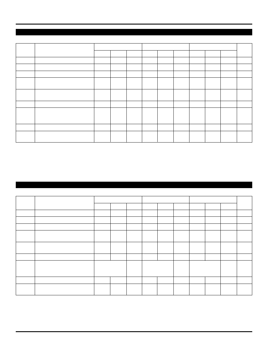
TIMING DIAGRAM
Q
CLK
t
RR
RESET