
DESCRIPTION
FEATURES
Rev.: D
Amendment: /0
Rev. Date:
October, 1998
ClockWorksTM
SY10E111AE/LE
SY100E111AE/LE
5V/3.3V 1:9 DIFFERENTIAL
CLOCK DRIVER (w/ENABLE)
s
5V and 3.3V power supply options
s
200ps part-to-part skew
s
50ps output-to-output skew
s
Differential design
s
V
BB
output
s
Enable Input
s
Voltage and temperature compensated outputs
s
75K
input pulldown resistors
s
Fully compatible with Motorola MC10/100E111
s
Available in 28-pin PLCC package
The SY10/100E111AE/LE are low skew 1-to-9 differential
drivers designed for clock distribution in mind. The SY10/
100E111AE/LE's function and performance are similar to
the popular SY10/100E111, with the improvement of lower
jitter and the added feature of low voltage operation. It
accepts one signal input, which can be either differential or
single-ended if the V
BB
output is used. The signal is fanned
out to 9 identical differential outputs. An enable input is
also provided such that a logic HIGH disables the device by
forcing all Q outputs LOW and all Q outputs HIGH.
The E111AE/LE is specifically designed, modeled and
produced with low skew as the key goal. Optimal design
and layout serve to minimize gate to gate skew within a
device, and empirical modeling is used to determine process
control limits that ensure consistent t
pd
distributions from
lot to lot. The net result is a dependable, guaranteed low
skew device.
To ensure that the tight skew specification is met it is
necessary that both sides of the differential output are
terminated into 50
, even if only one side is being used. In
most applications, all nine differential pairs will be used
and therefore terminated. In the case where fewer that
nine pairs are used, it is necessary to terminate at least the
output pairs on the same package side as the pair(s) being
used on that side, in order to maintain minimum skew.
Failure to do this will result in small degradations of
propagation delay (on the order of 10-20ps) of the output(s)
being used which, while not being catastrophic to most
designs, will mean a loss of skew margin.
The E111AE/LE, as with most other ECL devices, can
be operated from a positive V
CC
supply in PECL mode.
This allows the E111AE/LE to be used for high performance
clock distribution in +5V/+3.3V systems. Designers can
take advantage of the E111AE/LE's performance to
distribute low skew clocks across the backplane or the
board. In a PECL environment, series or Thevenin line
terminations are typically used as they require no additional
power supplies. For systems incorporating GTL, parallel
termination offers the lowest power by taking advantage of
the 1.2V supply as terminating voltage.
BLOCK DIAGRAM
IN
V
BB
Q
0
Q
0
Q
1
Q
1
Q
2
Q
2
Q
3
Q
3
Q
4
Q
4
Q
5
Q
5
Q
6
Q
6
Q
7
Q
7
Q
8
Q
8
IN
EN
1

2
ClockWorksTM
SY10E111AE/LE
SY100E111AE/LE
Micrel
PIN CONFIGURATION
V
CC
V
EE
EN
V
BB
IN
Q
2
26
27
28
1
2
3
4
18
17
16
15
14
13
12
25 24 23 22 21 20 19
5
6
7
8
9
10 11
NC
IN
Q
6
Q
6
Q
3
Q
1
PLCC
TOP VIEW
J28-1
Q
2
Q
0
Q
0
V
CCO
Q
1
Q
3
Q
4
V
CCO
Q
4
Q
5
Q
5
Q
7
V
CCO
Q
7
Q
8
Q
8
Pin
Function
IN, IN
Differential Input Pair
EN
Enable Input
Q
0
, Q
0
-- Q
8
, Q
8
Differential Outputs
V
BB
V
BB
Output
V
CCO
V
CC
to Output
PIN NAMES
T
A
= �40
�
C
T
A
= 0
�
C
T
A
= +25
�
C
T
A
= +85
�
C
Symbol
Parameter
Min.
Typ.
Max.
Min.
Typ.
Max.
Min.
Typ.
Max.
Min.
Typ.
Max.
Unit
V
OH
Output HIGH Voltage
mV
10EL
�1080
--
�890
�1020
--
�840
�980
--
�810
�910
--
�720
100EL
�1085
--
�880
�1025
--
�880
�1025
--
�880
�1025
--
�880
V
OL
Output LOW Voltage
mV
10EL
�1950
--
�1650 �1950
--
�1630 �1950
--
�1630 �1950
--
�1595
100EL
�1830
--
�1550 �1810
--
�1620 �1810
--
�1620 �1810
--
�1620
V
IH
Input HIGH Voltage
mV
10EL
�1230
--
�890
�1170
--
�840
�1130
--
�810
�1060
--
�720
100EL
�1165
--
�880
�1165
--
�880
�1165
--
�880
�1165
--
�880
V
IL
Input LOW Voltage
mV
10EL
�1950
--
�1500 �1950
--
�1480 �1950
--
�1480 �1950
--
�1445
100EL
�1810
--
�1475 �1810
--
�1475 �1810
--
�1475 �1810
--
�1475
V
BB
Output Reference
V
Voltage
10EL
�1.43
--
�1.30
�1.38
--
�1.27
�1.35
--
�1.25
�1.31
--
�1.19
100EL
�1.38
--
�1.26
�1.38
--
�1.26
�1.38
--
�1.26
�1.38
--
�1.26
I
IH
Input HIGH Current
--
--
150
--
--
150
--
--
150
--
--
150
�
A
I
IL
Input LOW Current
�
A
10EL
0.5
--
--
0.5
--
--
0.5
--
--
0.3
--
--
100EL
0.5
--
--
0.5
--
--
0.5
--
--
0.5
--
--
I
EE
Power Supply Current
mA
10EL
--
--
66
--
--
66
--
--
66
--
--
66
100EL
--
--
66
--
--
66
--
--
66
--
--
78
ECL DC ELECTRICAL CHARACTERISTICS
V
EE
= V
EE
(Min.) to V
EE
(Max.); V
CC
= GND
NOTE:
1. Parametric values specified at:
5 volt Power Supply Range
100E111AE Series:
-4.2V to -5.5V.
10E111AE Series
-4.75V to -5.5V.
3 volt Power Supply Range
10/100E111LE Series: -3.0V to -3.8V.

3
ClockWorksTM
SY10E111AE/LE
SY100E111AE/LE
Micrel
3.3V PECL DC ELECTRICAL CHARACTERISTICS
(1)
V
CC
= +3.0V to +3.8V, V
EE
= GND
T
A
= �40
�
C
T
A
= 0
�
C
T
A
= +25
�
C
T
A
= +85
�
C
Symbol
Parameter
Min.
Typ.
Max.
Min.
Typ.
Max.
Min.
Typ.
Max.
Min.
Typ.
Max.
Unit
V
OH
Output HIGH Voltage
(2)
mV
10EL
2220
--
2110
2280
--
2460
2320
--
2490
2390
--
2580
100EL
2215
--
2120
2275
--
2420
2275
--
2420
2275
--
2420
V
OL
Output LOW Voltage
(2)
mV
10EL
1350
--
1650
1350
--
1670
1350
--
1670
1350
--
1705
100EL
1470
--
1750
1490
--
1680
1490
--
1680
1490
--
1680
V
IH
Input HIGH Voltage
(2)
mV
10EL
2070
--
2410
2130
--
2460
2170
--
2490
2240
--
2580
100EL
2135
--
2420
2135
--
2420
2135
--
2420
2135
--
2420
V
IL
Input LOW Voltage
(2)
mV
10EL
1350
--
1800
1350
--
1820
1350
--
1820
1350
--
1855
100EL
1490
--
1825
1490
--
1825
1490
--
1825
1490
--
1825
V
BB
Output Reference
V
Voltage
(2)
10EL
1.87
--
2.00
1.92
--
2.03
1.95
--
2.05
1.99
--
2.11
100EL
1.92
--
2.04
1.92
--
2.04
1.92
--
2.04
1.92
--
2.04
I
IH
Input HIGH Current
--
--
150
--
--
150
--
--
150
--
--
150
�
A
I
IL
Input LOW Current
�
A
10EL
0.5
--
--
0.5
--
--
0.5
--
--
0.3
--
--
100EL
0.5
--
--
0.5
--
--
0.5
--
--
0.5
--
--
I
EE
Power Supply Current
mA
10EL
--
--
66
--
--
66
--
--
66
--
--
66
100EL
--
--
66
--
--
66
--
--
66
--
--
78
NOTES:
1. Parametric values specified at:
3 volt Power Supply Range
10/100E111LE Series:
+3.0V to +3.8V.
2. These values are for V
CC
= 3.3V. Level specifications will vary 1:1 with V
CC.
5V PECL DC ELECTRICAL CHARACTERISTICS
(1)
V
CC
= V
CC
(Min.) to V
CC
(Max.); V
EE
= GND
T
A
= �40
�
C
T
A
= 0
�
C
T
A
= +25
�
C
T
A
= +85
�
C
Symbol
Parameter
Min.
Typ.
Max.
Min.
Typ.
Max.
Min.
Typ.
Max.
Min.
Typ.
Max.
Unit
V
OH
Output HIGH Voltage
(2)
mV
10EL
3920
--
4110
3980
--
4160
4020
--
4190
4090
--
4280
100EL
3915
--
4120
3975
--
4120
3975
--
4120
3975
--
4120
V
OL
Output LOW Voltage
(2)
mV
10EL
3050
--
3350
3050
--
3370
3050
--
3370
3050
--
3405
100EL
3170
--
3450
3190
--
3380
3190
--
3380
3190
--
3380
V
IH
Input HIGH Voltage
(2)
mV
10EL
3770
--
4110
3830
--
4160
3870
--
4190
3940
--
4280
100EL
3835
--
4120
3835
--
4120
3835
--
4120
3835
--
4120
V
IL
Input LOW Voltage
(2)
mV
10EL
3050
--
3500
3050
--
3520
3050
--
3520
3050
--
3555
100EL
3190
--
3525
3190
--
3525
3190
--
3525
3190
--
3525
V
BB
Output Reference
V
Voltage
(2)
10EL
3.57
--
3.70
3.62
--
3.73
3.65
--
3.75
3.69
--
3.81
100EL
3.62
--
3.74
3.62
--
3.74
3.62
--
3.74
3.62
--
3.74
I
IH
Input HIGH Current
--
--
150
--
--
150
--
--
150
--
--
150
�
A
I
IL
Input LOW Current
�
A
10EL
0.5
--
--
0.5
--
--
0.5
--
--
0.3
--
--
100EL
0.5
--
--
0.5
--
--
0.5
--
--
0.5
--
--
I
EE
Power Supply Current
mA
10EL
--
--
66
--
--
66
--
--
66
--
--
66
100EL
--
--
66
--
--
66
--
--
66
--
--
78
NOTES:
1. Parametric values specified at:
5 volt Power Supply Range
100E111AE Series:
+4.2V to +5.5V.
10E111AE Series
+4.75V to +5.5V.
2. These values are for V
CC
= 5V. Level specifications will vary 1:1 with V
CC.
4
ClockWorksTM
SY10E111AE/LE
SY100E111AE/LE
Micrel
V
EE
= V
EE
(Min.) to V
EE
(Max.); V
CC
= GND
T
A
= �40
�
C
T
A
= 0
�
C
T
A
= +25
�
C
T
A
= +85
�
C
Symbol
Parameter
Min.
Typ.
Max.
Min.
Typ.
Max.
Min.
Typ.
Max. Min.
Typ.
Max.
Unit
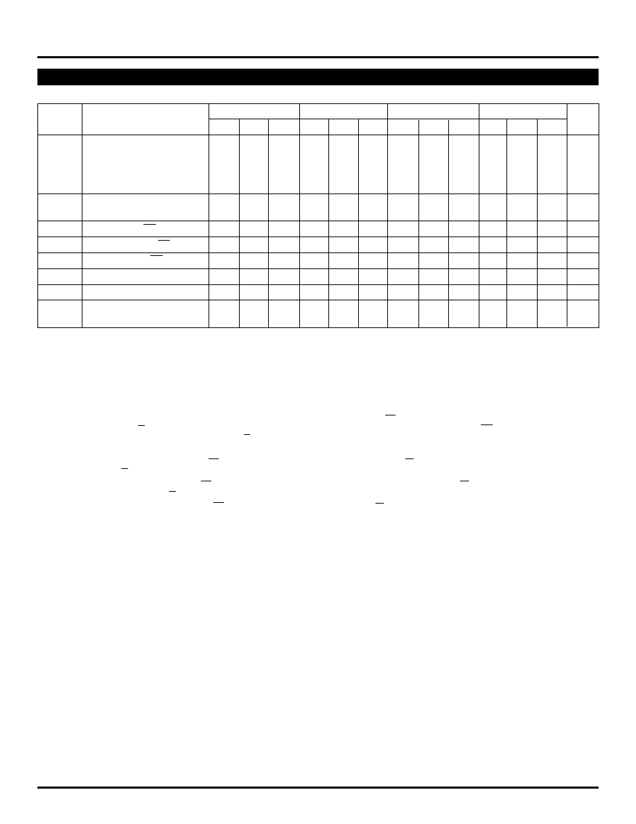
t
PLH
Propagation Delay to Output
ps
t
PHL
IN (differential)
(2)
380
--
680
430
--
630
430
--
630
430
--
630
IN (single-ended)
(3)
280
--
780
330
--
730
330
--
730
330
--
730
Enable
(4)
400
--
900
450
--
850
450
--
850
450
--
850
Disable
(4)
400
--
900
450
--
850
450
--
850
450
--
850
t
skew
Within-Device Skew
(5)
--
--
75
--
--
50
--
--
50
--
--
50
ps
Part-to-Part Skew (Diff.)
--
--
250
--
--
200
--
--
200
--
--
200
t
S
Set-up Time, EN to IN
(6)
250
--
0
200
0
--
200
0
--
200
0
--
ps
t
H
Hold Time, IN to EN
(7)
0
--
�200
0
�200
--
0
�200
--
0
�200
--
ps
t
R
Release Time, EN to IN
(8)
350
--
100
300
100
--
300
100
--
300
100
--
ps
V
PP
Minimum Input Swing
(9)
250
--
--
250
--
--
250
--
--
250
--
--
mV
V
CMR
Common Mode Range
(10)
�1.5
--
�0.4
�1.5
--
�0.4
�1.5
--
�0.4
�1.5
--
�0.4
V
t
r
Rise/Fall Times
200
--
650
200
--
600
200
--
600
200
--
600
ps
t
f
20% to 80%
NOTES:
1. Parametric values specified at:
5 volt Power Supply Range
100E111AE Series:
-4.2V to -5.5V.
10E111AE Series
-4.75V to -5.5V.
3 volt Power Supply Range
10/100E111LE Series: -3.0V to -3.8V.
2. The differential propagation delay is defined as the delay from the crossing points of the differential input signals to the crossing point of the
differential output signals.
3. The single-ended propagation delay is defined as the delay from the 50% point of the input signal to the 50% point of the output signal.
4. Enable is defined as the propagation delay from the 50% point of a negative transition on EN to the 50% point of a positive transition on Q (or a
negative transition on Q). Disable is defined as the propagation delay from the 50% point of a positive transition on EN to the 50% point of a
negative transition on Q (or a positive transition on Q).
5. The within-device skew is defined as the worst case difference between any two similar delay paths within a single device.
6. The set-up time is the minimum time that EN must be asserted prior to the next transition of IN/IN to prevent an output response greater than
�
75mV to that IN/IN transition (see Figure 1).
7. The hold time is the minimum time that EN must remain asserted after a negative going IN or a positive going IN to prevent an output response
greater than
�
75mV to that IN/IN transition (see Figure 2).
8. The release time is the minimum time that EN must be de-asserted prior to the next IN/IN transition to ensure an output response that meets the
specified IN to Q propagation delay and output transition times (see Figure 3).
9. V
PP
(min) is defined as the minimum input differential voltage which will cause no increase in the propagation delay. The V
PP
(min) is AC limited
for the E111AE/LE, as a differential input as low as 50mV will still produce full ECL levels at the output.
10. V
CMR
is defined as the range within the V
IH
level may vary, with the device still meeting the propagation delay specification. the V
IL
level must be
such that the peak-to-peak voltage is less than 1.0V and greater than or equal to V
PP
(min).
For PECL operation: V
CMR
(max) = V
CC
� |V
CMR
(max)| and
V
CMR
(min) = V
CC
� |V
CMR
(min)|
AC ELECTRICAL CHARACTERISTICS
(1)

5
ClockWorksTM
SY10E111AE/LE
SY100E111AE/LE
Micrel
Ordering
Package
Operating
V
EE
Range
Code
Type
Range
(V)
SY10E111AEJC
J28-1
Commercial
-4.75 to -5.5
SY10E111AEJCTR
J28-1
Commercial
-4.75 to -5.5
SY100E111AEJC
J28-1
Commercial
-4.2 to -5.5
SY100E111AEJCTR
J28-1
Commercial
-4.2 to -5.5
PRODUCT ORDERING CODE
5V
TIMING DIAGRAMS
Figure 1. Set-up Time
Figure 3. Release Time
Figure 2. Hold Time
SY10E111LEJC
J28-1
Commercial
-3.0 to -3.8
SY10E111LEJCTR
J28-1
Commercial
-3.0 to -3.8
SY100E111LEJC
J28-1
Commercial
-3.0 to -3.8
SY100E111LEJCTR
J28-1
Commercial
-3.0 to -3.8
3.3V
Ordering
Package
Operating
V
EE
Range
Code
Type
Range
(V)
SY10E111AEJI
J28-1
Industrial
-4.75 to -5.5
SY10E111AEJITR
J28-1
Industrial
-4.75 to -5.5
SY100E111AEJI
J28-1
Industrial
-4.2 to -5.5
SY100E111AEJITR
J28-1
Industrial
-4.2 to -5.5
5V
SY10E111LEJI
J28-1
Industrial
-3.0 to -3.8
SY10E111LEJITR
J28-1
Industrial
-3.0 to -3.8
SY100E111LEJI
J28-1
Industrial
-3.0 to -3.8
SY100E111LEJITR
J28-1
Industrial
-3.0 to -3.8
3.3V
IN
t
s
IN
EN
Q
Q
50%
75 mV
75 mV
IN
t
h
IN
EN
Q
Q
50%
75 mV
75 mV
IN
t
r
IN
EN
Q
Q
50%