FEATURES
s
450ps max. Propagation Delay
s
Extended 100E V
EE
range of ≠4.2V to ≠5.5V
s
V
BB
output for single-ended reception
s
Fully compatible with industry standard 10KH,
100K I/O levels
s
Internal 75K
input pulldown resistors
s
Fully compatible with Motorola MC10E/100E116
s
Available in 28-pin PLCC package
DESCRIPTION
The SY10/100E116 are quint differential line receivers
designed for use in new, high-performance ECL systems.
These devices have emitter-follower outputs and an
internally generated reference supply (V
BB
) for single-
ended reception.
Active current sources combined with Micrel-Synergy's
ASSETTM technology provide the receivers with excellent
common mode noise rejection.
The receiver design features clamp circuitry to cause a
defined output state if both the inverting and non-inverting
inputs are left open; in this case the Q output goes LOW,
while the Q output goes HIGH.
If both inverting and non-inverting inputs are at equal
potential, the receiver does
not go to a defined state, but
rather shares current in normal differential amplifier fashion,
producing output voltage levels midway between HIGH
and LOW.
The V
BB
output is intended for use as a reference
voltage for single-ended reception of ECL signals to that
device only. When using V
BB
for this purpose, it is
recommended that V
BB
is decoupled to V
CC
via a 0.01
µ
F
capacitor.
For higher bandwidth, please refer to the SY10/100E416
device.
QUINT DIFFERENTIAL
LINE RECEIVER
SY10E116
SY100E116
Rev.: E
Amendment: /0
Issue Date: November, 1998
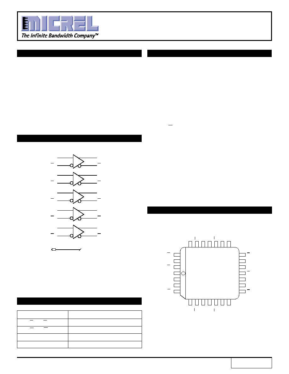
PIN CONFIGURATION
BLOCK DIAGRAM
Pin
Function
D
0
, D
0
-D
4
, D
4
Differential Input Pairs
Q
0
, Q
0
-Q
4
, Q
4
Differential Output Pairs
V
BB
Reference Voltage Output
V
CCO
V
CC
to Output
PIN NAMES
V
BB
Q
0
Q
0
Q
1
Q
1
Q
2
Q
2
Q
3
Q
3
Q
4
Q
4
D
0
D
0
D
1
D
1
D
2
D
2
D
3
D
3
D
4
D
4
D
4
V
EE
D
3
D
2
D
0
V
BB
Q
4
26
27
28
1
2
3
4
18
17
16
15
14
13
12
25
24
23 22
21
20
19
5
6
7
8
9
10
11
D
0
D
2
Q
1
V
CCO
Q
3
Q
4
PLCC
TOP VIEW
J28-1
D
3
V
CCO
D
4
Q
3
V
CC
Q
2
Q
2
V
CCO
Q
1
Q
0
Q
0
V
CCO
D
1
D
1
V
CCO
1

2
SY10E116
SY100E116
Micrel
PRODUCT ORDERING CODE
Ordering
Package
Operating
Code
Type
Range
SY10E116JC
J28-1
Commercial
SY10E116JCTR
J28-1
Commercial
SY100E116JC
J28-1
Commercial
SY100E116JCTR
J28-1
Commercial
NOTES:
1. Minimum input swing for which AC parameters are guaranteed.
2. Within-device skew is defined as identical transitions on similar paths through a device.
3. Duty cycle skew is defined only for differential operation when the delays are measured from the cross point of the inputs to the cross point of the
outputs.
DC ELECTRICAL CHARACTERISTICS
V
EE
= V
EE
(Min.) to V
EE
(Max.); V
CC
= V
CCO
= GND
T
A
= ≠40
∞
C
T
A
= 0
∞
C
T
A
= +25
∞
C
T
A
= +85
∞
C
Symbol
Parameter
Min.
Typ.
Max.
Min.
Typ.
Max.
Min.
Typ.
Max.
Min.
Typ.
Max.
Unit
V
BB
Output Reference
V
Voltage
10E
≠1.43
--
≠1.30
≠1.38
--
≠1.27
≠1.35
--
≠1.25
≠1.31
--
≠1.19
100E
≠1.43
--
≠1.26
≠1.38
--
≠1.26
≠1.38
--
≠1.26
≠1.38
--
≠1.26
I
IH
Input HIGH Current
--
--
200
--
--
200
--
--
200
--
--
200
µ
A
I
EE
Power Supply Current
mA
10E
--
29
35
--
29
35
--
29
35
--
29
35
100E
--
29
35
--
29
35
--
29
35
--
33
40
V
PP (DC)
Input Sensitivity
(1)
150
--
--
150
--
--
150
--
--
150
--
--
mV
V
CMR
Common Mode Range
(2)
≠2.0
--
≠0.6
≠2.0
--
≠0.6
≠2.0
--
≠0.6
≠2.0
--
≠0.6
V
NOTES:
1. V
PP
is the minimum differential input voltage required to assure full ECL levels are present at the outputs.
2. V
CMR
is referenced to the most positive side of the differential input signal. Normal operation is obtained when the "HIGH" input is within the V
CMR
range
and the input swing is greater than V
PP
(min.) and <1V.
AC ELECTRICAL CHARACTERISTICS
V
EE
= V
EE
(Min.) to V
EE
(Max.); V
CC
= V
CCO
= GND
T
A
= ≠40
∞
C
T
A
= 0
∞
C
T
A
= +25
∞
C
T
A
= +85
∞
C
Symbol
Parameter
Min.
Typ.
Max.
Min.
Typ.
Max.
Min.
Typ.
Max.
Min.
Typ.
Max.
Unit
t
PLH
Propagation Delay to
ps
t
PHL
Output
D
150
300
500
200
300
450
200
300
450
200
300
450
D (S.E.)
150
300
550
150
300
500
150
300
500
150
300
500
V
PP (DC)
Input Sensitivity
(1)
150
--
150
150
--
--
150
--
--
150
--
--
mV
t
skew
Within-Device Skew
(2)
--
50
--
--
50
--
--
50
--
--
50
--
ps
Dn to Qn, Qn
t
skew
Duty Cycle Skew
(3)
--
±
10
--
--
±
10
--
--
±
10
--
--
±
10
--
ps
t
PLH ≠
t
PHL
t
r
Rise/Fall Time
250
375
625
275
375
575
275
375
575
275
375
575
ps
t
f
20% to 80%
Q
n
= D
n
LOGIC EQUATION
Ordering
Package
Operating
Code
Type
Range
SY10E116JI
J28-1
Industrial
SY10E116JITR
J28-1
Industrial
SY100E116JI
J28-1
Industrial
SY100E116JITR
J28-1
Industrial

4
SY10E116
SY100E116
Micrel
MICREL-SYNERGY
3250 SCOTT BOULEVARD
SANTA CLARA
CA 95054
USA
TEL
+ 1 (408) 980-9191
FAX
+ 1 (408) 914-7878
WEB
http://www.micrel.com
This information is believed to be accurate and reliable, however no responsibility is assumed by Micrel for its use nor for any infringement of patents or
other rights of third parties resulting from its use. No license is granted by implication or otherwise under any patent or patent right of Micrel Inc.
© 2000 Micrel Incorporated