
DESCRIPTION
FEATURES
PROGRAMMABLE DELAY
CHIP WITH ANALOG INPUT
Rev.: E
Amendment: /0
Issue Date:
October, 1998
ClockWorksTM
SY10E196
SY100E196
s
Up to 2ns delay range
s
Extended 100E V
EE
range of ≠4.2V to ≠5.5V
s
20ps digital step resolution
s
Linear input for tighter resolution
s
>1GHz bandwidth
s
On-chip cascade circuitry
s
75Kk
input pulldown resistor
s
Fully compatible with Motorola MC10E/100E196
s
Available in 28-pin PLCC package
The SY10/100E196 are programmable delay chips
(PDCs) designed primarily for very accurate differential
ECL input edge placement applications.
The delay section consists of a chain of gates and a
linear ramp delay adjustment organized as shown in the
logic diagram. The first two delay elements feature gates
that have been modified to have delays 1.25 and 1.5
times the basic gate delay of approximately 80ps. These
two elements provide the E196 with a digitally-selectable
resolution of approximately 20ps. The required device
delay is selected by the seven address inputs D[0:6],
which are latched on-chip by a high signal on the latch
enable (LEN) control. If the LEN signal is either LOW or
left floating, then the latch is transparent.
The FTUNE input takes an analog coltage and applies
it to an internal linear ramp for reducing the 20s resolution
still further. The FTUNE input is what differentiates the
E196 from the E195.
An eighth latched input, D7, is provided for cascading
multiple PDCs for increased programmable range. The
cascade logic allows full control of multiple PDCs, at the
expense of only a single added line to the data bus for
each additional PDC, without the need for any external
gating.
Pin
Function
IN/IN
Signal Input
EN
Input Enable
D[0:7]
Mux Select Inputs
Q/Q
Signal Output
LEN
Latch Enable
SET MIN
Minimum Delay Set
SET MAX
Maximum Delay Set
CASCADE
Cascade Signal
FTUNE
Linear Voltage Input
V
CCO
V
CC
to Output
PIN NAMES
PIN CONFIGURATION
18
17
16
15
14
13
12
5
6
7
8
9
10 11
26
27
28
1
2
3
4
TOP VIEW
PLCC
J28-1
25 24 23 22 21 20 19
D
4
D
5
D
6
D
7
D
2
D
3
NC
D
1
D
0
LEN
V
EE
IN
V
BB
IN
NC
NC
SET MIN
SET MAX
CASCADE
EN
CASCADE
FTUNE
NC
V
CC
V
CCO
Q
V
CCO
Q
1
4
ClockWorksTM
SY10E196
SY100E196
Micrel
NOTES:
1. Duty cycle skew guaranteed only for differential operation measured from the cross point of the input to the cross point of the output.
2. This set-up time defines the amount of time prior to the input signal the delay tap of the device must be set.
3. This set-up time is the minimum time that EN must be asserted prior to the next transition of IN/IN to prevent an output response greater than
±
75mV to
that IN/IN transition.
4. This hold time is the minimum time that EN must remain asserted after a negative going IN or positive going IN to prevent an output response greater than
±
75mV to that IN/IN transition.
5. This release time is the minimum time that EN must be deasserted prior to the next IN/IN transition to ensure an output response that meets the specified
IN to Q propagation delay and transition times.
6. Specification limits represent the amount of delay added with the assertion of each individual delay control pin. The various combinations of asserted delay
control inputs will typically realize D
0
resolution steps across the specified programmable range.
7. The linearity specification guarantees to which delay control input the programmable steps will be monotonic (i.e. increasing delay steps for increasing
binary counts on the control inputs D
n
). Typically, the device will be monotonic to the D
0
input, however, under worst case conditions and process variation,
delays could decrease slightly with increasing binary counts when the D
0
input is the LSB. With the D
1
input as the LSB, the device is guaranteed to be
monotonic over all specified environmental conditions and process variation.
8. The jitter of the device is less than what can be measured without resorting to very tedious and specialized measurement techniques.
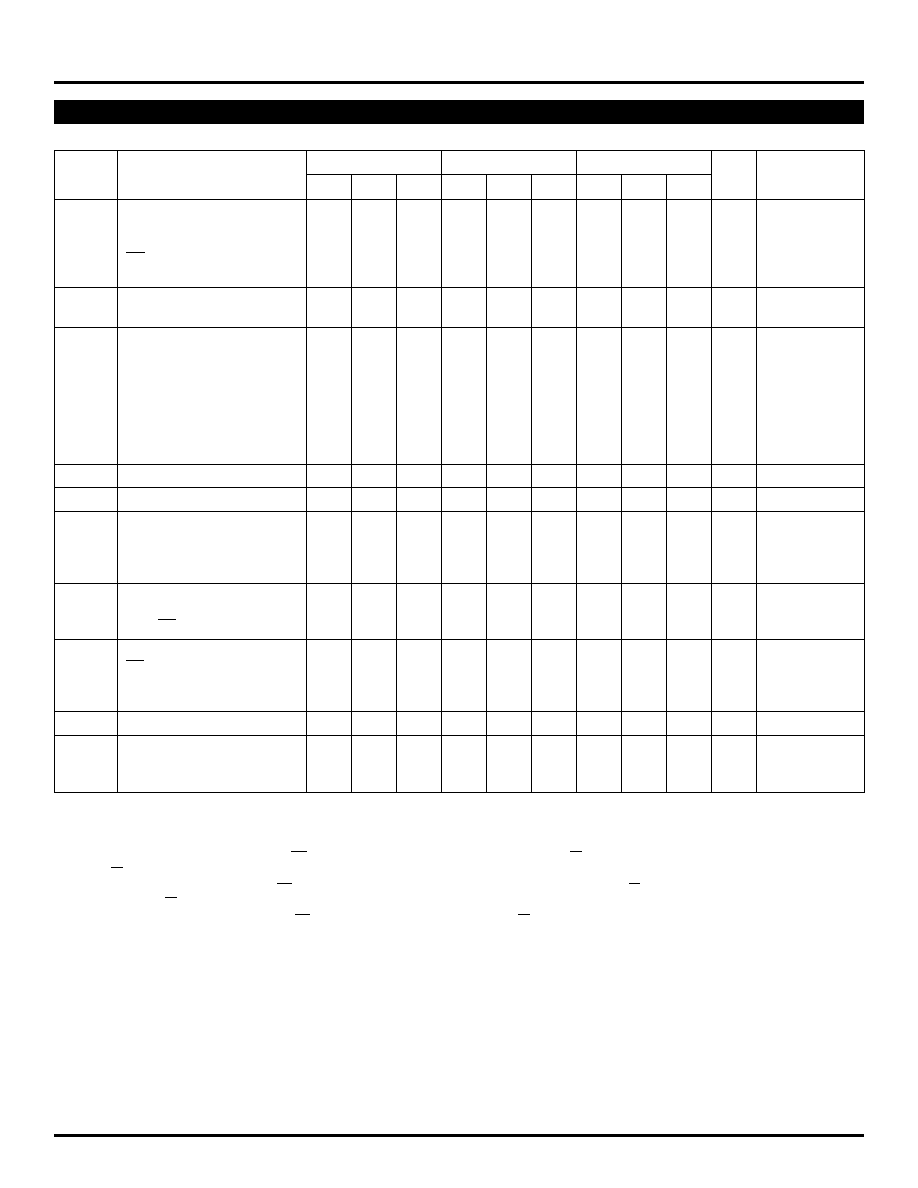
T
A
= 0
∞
C
T
A
= +25
∞
C
T
A
= +85
∞
C
Symbol
Parameter
Min.
Typ.
Max.
Min.
Typ.
Max.
Min.
Typ.
Max.
Unit
Condition
t
PLH
Propagation Delay to Output
ps
--
t
PHL
IN to Q; Tap = 0
1210
1360
1510
1240
1390
1540
1440
1590
1765
IN to Q; Tap = 127
3320
3570
3820
3380
3630
3880
3920
4270
4720
EN to Q; Tap = 0
1250
1450
1650
1275
1475
1675
1350
1650
1950
D
7
to CASCADE
300
450
700
300
450
700
300
450
700
t
RANGE
Programmable Range
2000
2175
--
2050
2240
--
2375
2580
--
ps
--
t
PD
(max.) ≠ t
PD
(min.)
t
Step Delay
ps
6
D
0
High
--
17
--
--
17.5
--
--
21
--
D
1
High
--
34
--
--
35
--
--
42
--
D
2
High
55
68
105
55
70
105
65
84
120
D
3
High
115
136
180
115
140
180
140
168
205
D
4
High
250
272
325
250
280
325
305
336
380
D
5
High
505
544
620
515
560
620
620
672
740
D
6
High
1000
1088
1190
1030
1120
1220
1240
1344
1450
Lin
Linearity
D
1
D
0
--
D
1
D
0
--
D
1
D
0
--
--
7
t
skew
Duty Cycle Skew, t
PHL
≠t
PLH
--
±
30
--
--
±
30
--
--
±
30
--
ps
1
t
S
Set-up Time
ps
D to LEN
200
0
--
200
0
--
200
0
--
D to IN
800
--
--
800
--
--
800
--
--
2
EN to IN
200
--
--
200
--
--
200
--
--
3
t
H
Hold Time
ps
LEN to D
500
250
--
500
250
--
500
250
--
IN to EN
0
--
--
0
--
--
0
--
--
4
t
R
Release Time
ps
EN to IN
300
--
--
300
--
--
300
--
--
5
SET MAX to LEN
800
--
--
800
--
--
800
--
--
SET MIN to LEN
800
--
--
800
--
--
800
--
--
t
jit
Jitter
--
<5
--
--
<5
--
--
<5
--
ps
8
t
r
Rise/Fall Times
ps
--
t
f
20≠80% (Q)
125
225
325
125
225
325
125
225
325
20≠80% (CASCADE)
300
450
650
300
450
650
300
450
650
AC ELECTRICAL CHARACTERISTICS
V
EE
= V
EE
(Min.) to V
EE
(Max.); V
CC
= V
CCO
= GND


