
1
DESCRIPTION
FEATURES
2.5V/3.3V/5V 1:2 DIFFERENTIAL
PECL/LVPECL/ECL
FANOUT BUFFER
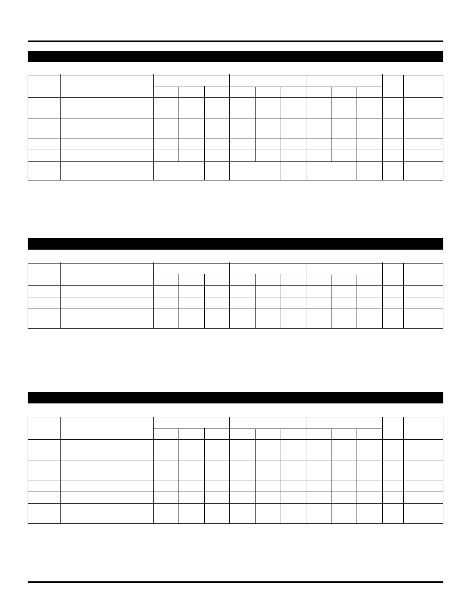
PIN CONFIGURATION/BLOCK DIAGRAM
1
2
3
4
5
6
7
8
Q0
Q1
VCC
D
VEE
/D
/Q0
/Q1
V
EE
V
CC
V
EE
V
CC
75k
75k
75k
V
EE
8-pin MSOP and SOIC Packages
ECL ProTM
SY10EP11U
SY100EP11U
FINAL
s
2.5V, 3.3V and 5V power supply options
s
Guaranteed AC parameters over temperature:
∑ f
MAX
> 3.0GHz
∑ < 20ps output-to-output skew
∑ < 200ps t
r
/ t
f
∑ < 300ps propagation delay
s
Wide temperature range: ≠40
∞
C to +85
∞
C
s
Available in 8-pin (3mm) MSOP and SOIC packages
The SY10/100EP11U is a precision, high-speed 1:2
differential fanout buffer. Having within-device skews and
output transition times significantly improved over the
EL11V, the EP11U is ideally suited for those applications
which require the ultimate in AC performance.
The differential inputs of the EP11U employ clamping
circuitry to maintain stability under open input conditions.
If the inputs are left open, the Q outputs will go LOW.
Rev.: D
Amendment: /0
Issue Date:
March 2003
Pin
Function
D
PECL, LVPECL, ECL, LVECL Clock or Data Input:
Internal 75k
pulldown resistor. If left floating,
pin defaults LOW, Q
OUT
goes LOW.
/D
PECL, LVPECL, ECL, LVECL complementary
Clock or Data Input: Internal 75k
pull-up and
down resistors. If left open, default is V
CC
/2. When
the input is not used, it can be left open.
Q0, /Q0
PECL, LVPECL, ECL, LVECL Outputs:
Q1, /Q1
Terminates to V
CC
≠2V.
V
CC
Positive Power Supply: Bypass with 0.1
µ
F//0.01
µ
F
low ESR capacitors.
V
EE
Negative Power Supply: For PECL operation,
connect to GND.
PIN NAMES
Micrel Semiconductor
ON Semiconductor
SY10EP11UZI/KI
MC10EP11D/DT
SY10EP11UZI/KI
MC10LVEP11D/DT
SY100EP11UZI/KI
MC100EP11D/DT
SY100EP11UZI/KI
MC100LVEP11D/DT
CROSS REFERENCE TABLE
ECL ProTM
ECL Pro is a trademark of Micrel, Inc.

2
ECL ProTM
SY10EP11U
SY100EP11U
Micrel
Symbol
Rating
Value
Unit
V
CC
-- V
EE
Power Supply Voltage
6V
V
V
IN
Input Voltage (V
CC
= 0V, V
IN
not more negative than V
EE
)
≠6.0 to 0
V
Input Voltage (V
EE
= 0V, V
IN
not more positive than V
CC
)
+6.0 to 0
V
I
OUT
Output Current
≠Continuous
50
mA
≠Surge
100
T
A
Operating Temperature Range
≠40 to +85
∞
C
T
store
Storage Temperature Range
≠65 to +150
∞
C
JA
Package Thermal Resistance
≠Still-Air
(SOIC)
160
∞
C/W
(Junction-to-Ambient)
≠500lfpm
(SOIC)
109
≠Still-Air
(MSOP)
206
∞
C/W
≠500lfpm
(MSOP)
155
JC
Package Thermal Resistance
(SOIC)
39
∞
C/W
(Junction-to-Case)
(MSOP)
39
Note 1.
Permanent device damage may occur if ABSOLUTE MAXIMUM RATINGS are exceeded. This is a stress rating only and functional operation
is not implied at conditions other than those detailed in the operational sections of this data sheet. Exposure to ABSOLUTE MAXIMUM
RATlNG conditions for extended periods may affect device reliability.
ABSOLUTE MAXIMUM RATINGS
(1)
T
A
= ≠40
∞
C
T
A
= +25
∞
C
T
A
= +85
∞
C
Symbol
Parameter
Min.
Typ.
Max.
Min.
Typ.
Max.
Min.
Typ.
Max.
Unit
Condition
V
CC
Power Supply Voltage
V
(PECL)
4.5
5.0
5.5
4.5
5.0
5.5
4.5
5.0
5.5
(LVPECL)
2.37
--
3.8
2.37
--
3.8
2.37
--
3.8
(ECL)
≠5.5
≠5.0
≠4.5
≠5.5
≠5.0
≠4.5
≠5.5
≠5.0
≠4.5
(LVECL)
≠3.8
≠3.3
≠2.37
≠3.8
≠3.3
≠2.37
≠3.8
≠3.3
≠2.37
I
EE
Power Supply Current
SY10EP11U
--
--
37
--
25
39
--
--
40
mA
SY100EP11U
--
--
44
--
30
44
--
--
44
mA
I
IH
Input HIGH Current
--
--
150
--
--
150
--
--
150
µ
A
V
IN
= V
IH
I
IL
Input LOW Current
D
0.5
--
--
0.5
--
--
0.5
--
--
µ
A
V
IN
= V
IL
/D
≠150
--
--
≠150
--
--
≠150
--
--
µ
A
V
IN
= V
IL
C
IN
Input Capacitance (MSOP)
--
--
--
--
1.0
--
--
--
--
pF
(SOIC)
--
--
--
--
1.35
--
--
--
--
pF
Note 1.
10/100KEP circuits are designed to meet the DC specifications shown in the above table after thermal equilibrium has been established. The
circuit is in a test socket or mounted on a printed circuit board and traverse airflow greater than 500lfpm is maintained.
DC ELECTRICAL CHARACTERISTICS
(1)

3
ECL ProTM
SY10EP11U
SY100EP11U
Micrel
T
A
= ≠40
∞
C
T
A
= +25
∞
C
T
A
= +85
∞
C
Symbol
Parameter
Min.
Typ.
Max.
Min.
Typ.
Max.
Min.
Typ.
Max.
Unit
Condition
V
OL
Output LOW Voltage
565
690
815
630
755
880
690
815
940
mV
50
to V
CC
≠2V
V
OH
Output HIGH Voltage
1365
1490
1615
1430
1555
1680
1490
1615
1740
mV
50
to V
CC
≠2V
V
IHCMR
Input HIGH Voltage
(2)
1.2
--
V
CC
1.2
--
V
CC
1.2
--
V
CC
V
Common Mode Range
(10KEP) LVPECL DC ELECTRICAL CHARACTERISTICS
(1)
V
CC
= 2.5V
±
5%, V
EE
= 0V
T
A
= ≠40
∞
C
T
A
= +25
∞
C
T
A
= +85
∞
C
Symbol
Parameter
Min.
Typ.
Max.
Min.
Typ.
Max.
Min.
Typ.
Max.
Unit
Condition
V
IL
Input LOW Voltage
1365
--
1690
1430
--
1755
1490
--
1815
mV
(Single-Ended)
V
IH
Input HIGH Voltage
2090
--
2415
2155
--
2480
2215
--
2540
mV
(Single-Ended)
V
OL
Output LOW Voltage
1365
1490
1615
1430
1555
1680
1490
1615
1740
mV
50
to V
CC
≠2V
V
OH
Output HIGH Voltage
2165
2290
2415
2230
2355
2480
2290
2415
2540
mV
50
to V
CC
≠2V
V
IHCMR
Input HIGH Voltage
(2)
1.2
--
V
CC
1.2
--
V
CC
1.2
--
V
CC
V
Common Mode Range
(10KEP) LVPECL DC ELECTRICAL CHARACTERISTICS
(1)
V
CC
= 3.3V
±
10%, V
EE
= 0V
No te 1. 10KEP circuits are designed to meet the DC specifications shown in the above table after thermal equilibrium has been established. The
circuit is in a test socket or mounted on a printed circuit board and traverse airflow greater than 500lfpm is maintained. Input and output
parameters are at V
CC
= 2.5V. They vary 1:1 with V
CC
.
Note 2.
The V
IHCMR
range is referenced to the most positive side of the differential input signal. See "Input Waveform" section. Single-ended input
CLK pin operation is limited to V
CC
3.0V in PECL mode.
Note 1.
10KEP circuits are designed to meet the DC specifications shown in the above table after thermal equilibrium has been established. The
circuit is in a test socket or mounted on a printed circuit board and traverse airflow greater than 500lfpm is maintained. Input and output
parameters are at V
CC
= 3.3V. They vary 1:1 with V
CC
.
Note 2.
The V
IHCMR
range is referenced to the most positive side of the differential input signal. See "Input Waveform" section. Single-ended input
CLK pin operation is limited to V
CC
3.0V in PECL mode.
T
A
= ≠40
∞
C
T
A
= +25
∞
C
T
A
= +85
∞
C
Symbol
Parameter
Min.
Typ.
Max.
Min.
Typ.
Max.
Min.
Typ.
Max.
Unit
Condition
V
IL
Input LOW Voltage
3065
--
3390
3130
--
3455
3190
--
3515
mV
(Single-Ended)
V
IH
Input HIGH Voltage
3790
--
4115
3855
--
4180
3915
--
4240
mV
(Single-Ended)
V
OL
Outuput LOW Voltage
3065
3190
3315
3130
3255
3380
3190
3315
3440
mV
50
to V
CC
≠2V
V
OH
Output HIGH Voltage
3865
3990
4115
3930
4055
4180
3990
4115
4240
mV
50
to V
CC
≠2V
V
IHCMR
Input HIGH Voltage
(2)
1.2
--
V
CC
1.2
--
V
CC
1.2
--
V
CC
V
Common Mode Range
(10KEP) PECL DC ELECTRICAL CHARACTERISTICS
(1)
V
CC
= 5.0V
±
10%, V
EE
= 0V
Note 1.
10KEP circuits are designed to meet the DC specifications shown in the above table after thermal equilibrium has been established. The
circuit is in a test socket or mounted on a printed circuit board and traverse airflow greater than 500lfpm is maintained. Input and output
parameters are at V
CC
= 5.0V. They vary 1:1 with V
CC
.
Note 2.
The V
IHCMR
range is referenced to the most positive side of the differential input signal. See "Input Waveform" section. Single-ended input
CLK pin operation is limited to V
CC
3.0V in PECL mode.
4
ECL ProTM
SY10EP11U
SY100EP11U
Micrel
T
A
= ≠40
∞
C
T
A
= +25
∞
C
T
A
= +85
∞
C
Symbol
Parameter
Min.
Typ.
Max.
Min.
Typ.
Max.
Min.
Typ.
Max.
Unit
Condition
V
IL
Input LOW Voltage
≠1935
--
≠1610 ≠1870
--
≠1545 ≠1810
--
≠1485
mV
(Single-Ended)
V
IH
Input HIGH Voltage
≠1210
--
≠885
≠1145
--
≠820
≠1085
--
≠760
mV
(Single-Ended)
V
OL
Outuput LOW Voltage
≠1935 ≠1810 ≠1685 ≠1870 ≠1745 ≠1620 ≠1810 ≠1685 ≠1560
mV
50
to V
CC
≠2V
V
OH
Output HIGH Voltage
≠1135 ≠1010
≠885
≠1070
≠945
≠820
≠1010
≠885
≠760
mV
50
to V
CC
≠2V
V
IHCMR
Input HIGH Voltage
(2)
V
EE
+1.2
0.0
V
EE
+1.2
0.0
V
EE
+1.2
0.0
V
Common Mode Range
(10KEP) ECL/LVECL DC ELECTRICAL CHARACTERISTICS
(1)
V
CC
= 0V, V
EE
= ≠5.5V to ≠2.375V
Note 1.
10KEP circuits are designed to meet the DC specifications shown in the above table after thermal equilibrium has been established. The
circuit is in a test socket or mounted on a printed circuit board and traverse airflow greater than 500lfpm is maintained.
Note 2.
The V
IHCMR
range is referenced to the most positive side of the differential input signal. See "Input Waveform" section. Single-ended input
CLK pin operation is limited to V
EE
≠3.0V in ECL/LVECL mode.
T
A
= ≠40
∞
C
T
A
= +25
∞
C
T
A
= +85
∞
C
Symbol
Parameter
Min.
Typ.
Max.
Min.
Typ.
Max.
Min.
Typ.
Max.
Unit
Condition
V
OL
Outuput LOW Voltage
555
680
805
555
680
805
555
680
805
mV
50
to V
CC
≠2V
V
OH
Output HIGH Voltage
1355
1480
1605
1355
1480
1605
1355
1480
1605
mV
50
to V
CC
≠2V
V
IHCMR
Input HIGH Voltage
(2)
1.2
--
V
CC
1.2
--
V
CC
1.2
--
V
CC
V
Common Mode Range
(100KEP) LVPECL DC ELECTRICAL CHARACTERISTICS
(1)
V
CC
= 2.5V
±
5%
Note 1.
100KEP circuits are designed to meet the DC specifications shown in the above table after thermal equilibrium has been established. The
circuit is in a test socket or mounted on a printed circuit board and traverse airflow greater than 500lfpm is maintained. Input and output
parameters are at V
CC
= 2.5V. They vary 1:1 with V
CC
.
Note 2.
The V
IHCMR
range is referenced to the most positive side of the differential input signal. See "Input Waveform" section. Single-ended input
CLK pin operation is limited to V
CC
3.0V in PECL mode.
T
A
= ≠40
∞
C
T
A
= +25
∞
C
T
A
= +85
∞
C
Symbol
Parameter
Min.
Typ.
Max.
Min.
Typ.
Max.
Min.
Typ.
Max.
Unit
Condition
V
IL
Input LOW Voltage
1355
--
1675
1355
--
1675
1355
--
1675
mV
(Single-Ended)
V
IH
Input HIGH Voltage
2075
--
2420
2075
--
2420
2075
--
2420
mV
(Single-Ended)
V
OL
Output LOW Voltage
1355
1480
1605
1355
1480
1605
1355
1480
1605
mV
50
to V
CC
≠2V
V
OH
Output HIGH Voltage
2155
2280
2405
2155
2280
2405
2155
2280
2405
mV
50
to V
CC
≠2V
V
IHCMR
Input HIGH Voltage
(2)
1.2
--
V
CC
1.2
--
V
CC
1.2
--
V
CC
V
Common Mode Range
(100KEP) LVPECL DC ELECTRICAL CHARACTERISTICS
(1)
V
CC
= 3.3V
±
10%, V
EE
= 0V
Note 1.
100KEP circuits are designed to meet the DC specifications shown in the above table after thermal equilibrium has been established. The
circuit is in a test socket or mounted on a printed circuit board and traverse airflow greater than 500lfpm is maintained. Input and output
parameters are at V
CC
= 3.3V. They vary 1:1 with V
CC
.
Note 2.
The V
IHCMR
range is referenced to the most positive side of the differential input signal. See "Input Waveform" section. Single-ended input
CLK pin operation is limited to V
CC
3.0V in PECL mode.

5
ECL ProTM
SY10EP11U
SY100EP11U
Micrel
T
A
= ≠40
∞
C
T
A
= +25
∞
C
T
A
= +85
∞
C
Symbol
Parameter
Min.
Typ.
Max.
Min.
Typ.
Max.
Min.
Typ.
Max.
Unit
Condition
V
IL
Input LOW Voltage
3055
--
3375
3055
--
3375
3055
--
3375
mV
(Single-Ended)
V
IH
Input HIGH Voltage
3775
--
4120
3775
--
4120
3775
--
4120
mV
(Single-Ended)
V
OL
Outuput LOW Voltage
3055
3180
3305
3055
3180
3305
3055
3180
3305
mV
50
to V
CC
≠2V
V
OH
Output HIGH Voltage
3855
3980
4105
3855
3980
4105
3855
3980
4105
mV
50
to V
CC
≠2V
V
IHCMR
Input HIGH Voltage
(2)
2.0
--
V
CC
2.0
--
V
CC
2.0
--
V
CC
V
Common Mode Range
(100KEP) PECL DC ELECTRICAL CHARACTERISTICS
(1)
V
CC
= 5.0V
±
10%, V
EE
= 0V
Note 1.
100KEP circuits are designed to meet the DC specifications shown in the above table after thermal equilibrium has been established. The
circuit is in a test socket or mounted on a printed circuit board and traverse airflow greater than 500lfpm is maintained. Input and output
parameters are at V
CC
= 5.0V. They vary 1:1 with V
CC
.
Note 2.
The V
IHCMR
range is referenced to the most positive side of the differential input signal. See "Input Waveform" section. Single-ended input
CLK pin operation is limited to V
CC
3.0V in PECL mode.
T
A
= ≠40
∞
C
T
A
= +25
∞
C
T
A
= +85
∞
C
Symbol
Parameter
Min.
Typ.
Max.
Min.
Typ.
Max.
Min.
Typ.
Max.
Unit
Condition
V
IL
Input LOW Voltage
≠1945
--
≠1625 ≠1945
--
≠1625 ≠1945
--
≠1625
mV
(Single-Ended)
V
IH
Input HIGH Voltage
≠1225
--
≠880
≠1225
--
≠880
≠1225
--
≠880
mV
(Single-Ended)
V
OL
Outuput LOW Voltage
≠1945 ≠1820 ≠1695 ≠1945 ≠1820 ≠1695 ≠1945 ≠1820 ≠1695
mV
50
to V
CC
≠2V
V
OH
Output HIGH Voltage
≠1145 ≠1020
≠895
≠1145 ≠1020
≠895
≠1145 ≠1020
≠895
mV
50
to V
CC
≠2V
V
IHCMR
Input HIGH Voltage
(2)
V
EE
+1.2
0.0
V
EE
+1.2
0.0
V
EE
+1.2
0.0
V
Common Mode Range
(100KEP) ECL/LVECL DC ELECTRICAL CHARACTERISTICS
(1)
V
CC
= 0V, V
EE
= ≠5.5V to ≠2.375V
Note 1.
100KEP circuits are designed to meet the DC specifications shown in the above table after thermal equilibrium has been established. The
circuit is in a test socket or mounted on a printed circuit board and traverse airflow greater than 500lfpm is maintained.
Note 2.
The V
IHCMR
range is referenced to the most positive side of the differential input signal. See "Input Waveform" section. Single-ended input
CLK pin operation is limited to V
EE
≠3.0V in ECL/LVECL mode.