1
ECL ProTM
SY10EP89V
Micrel
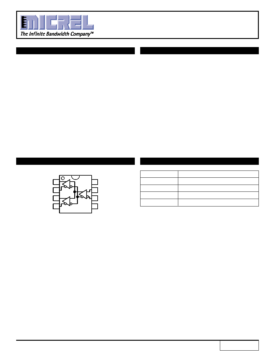
Pin
Function
D, /D
ECL Data Inputs
Q0, Q1, /Q0, /Q1
ECL Data Outputs
V
CC
Positive Supply
V
EE
Negative Supply
DESCRIPTION
s
3.3V and 5V power supply options
s
3.0GHz typical toggle frequency
s
310ps typical propagation delay
s
1.6V (5V) and 1.4V (3.3V) swing
s
Internal input resistors: pulldown on D, pulldown
and pullup on /D
s
New differential input common mode range
s
Available in 8-pin MSOP and SOIC packages
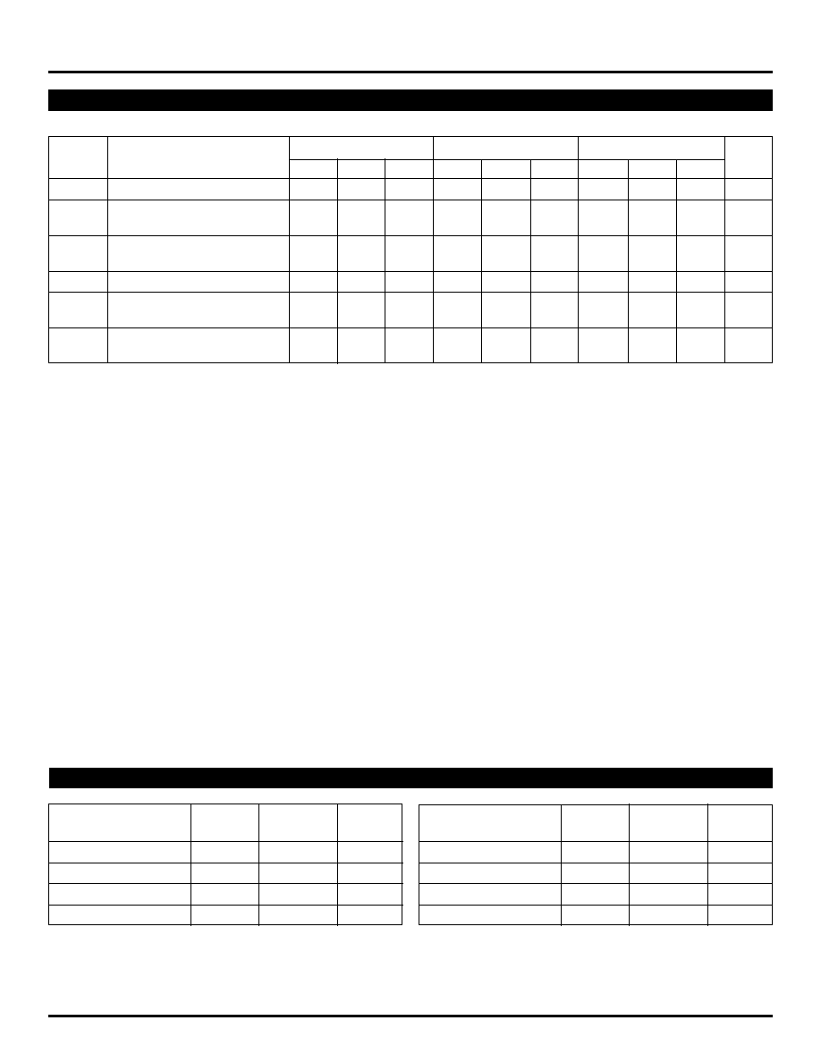
The SY10EP89V is a differential fanout gate specifically
designed to drive coaxial cables. The device is especially
useful in digitial video broadcasting applications; for this
application, since the system is polarity free, each output
can be used as an independent driver. The driver
produces swings 70% larger than a standard ECL output.
When driving a coaxial cable, proper termination is
required at both ends of the line, while maintaining a
800mV (5V) or 700mV (3.3V) swing at the receiving end
of the cable. Because of the larger output swings, the
device cannot be terminated into the standard V
CC
�2.0V.
All of the DC parameters are tested with a 50
to
V
CC
�3.0V load. The driver accepts a standard differential
ECL input and can run off of the digital video broadcast
standard �5.0V supply.
FEATURES
5V/3.3V 3GHz
COAXIAL CABLE DRIVER
PIN NAMES
PIN CONFIGURATION/BLOCK DIAGRAM
ECL ProTM
SY10EP89V
FINAL
Rev.: C
Amendment: /0
Issue Date:
March 2003
1
Q0
/Q0
Q1
/Q1
8
V
CC
D
/D
V
EE
7
6
5
2
3
4
Available in 8-Pin SOIC and MSOP Packages
ECL Pro is a trademark of Micrel, Inc.

2
ECL ProTM
SY10EP89V
Micrel
150
150
SY10EP89
V
EE
DC Blocking Capacitors
75
75
75
75
75
Coax
75
Coax
Figure 1. EP89V Termination Configuration
Symbol
Rating
Value
Unit
V
CC
-- V
EE
Power Supply Voltage
6V
V
V
IN
Input Voltage (V
CC
= 0V, V
IN
not more negative than V
EE
)
�6.0 to 0
V
Input Voltage (V
EE
= 0V, V
IN
not more positive than V
CC
)
+6.0 to 0
V
I
OUT
Output Current
�Continuous
50
mA
�Surge
100
T
A
Operating Temperature Range
�40 to +85
�
C
T
store
Storage Temperature Range
�65 to +150
�
C
JA
Package Thermal Resistance
�Still-Air
(SOIC)
160
�
C/W
(Junction-to-Ambient)
�500lfpm (SOIC)
109
�Still-Air
(MSOP)
206
�
C/W
�500lfpm (MSOP)
155
JC
Package Thermal Resistance
(SOIC)
39
�
C/W
(Junction-to-Case)
(MSOP)
39
Note 1.
Permanent device damage may occur if ABSOLUTE MAXIMUM RATINGS are exceeded. This is a stress rating only and functional operation
is not implied at conditions other than those detailed in the operational sections of this data sheet. Exposure to ABSOLUTE MAXIMUM
RATlNG conditions for extended periods may affect device reliability.
ABSOLUTE MAXIMUM RATINGS
(1)

3
ECL ProTM
SY10EP89V
Micrel
T
A
= �40
�
C
T
A
= +25
�
C
T
A
= +85
�
C
Symbol
Parameter
Min.
Typ.
Max.
Min.
Typ.
Max.
Min.
Typ.
Max.
Unit
I
EE
Power Supply Current
22
28
34
24
32
38
28
34
40
mA
V
OH
Output HIGH Voltage
(3)
2080
2180
2280
2150
2250
2350
2225
2325
2425
mV
V
OL
Outuput LOW Voltage
(3)
620
720
820
630
730
830
670
770
870
mV
V
IH
Input HIGH Voltage
2070
--
2410
2170
--
2490
2240
--
2580
mV
(Single-Ended)
V
IL
Input LOW Voltage
1350
--
1800
1350
--
1820
1350
--
1855
mV
(Single-Ended)
V
IHCMR
Input HIGH Voltage
V
EE
+2.0
V
CC
V
EE
+2.0
V
CC
V
EE
+2.0
V
CC
V
Common Mode Range (Diff.)
(4)
I
IH
Input HIGH Current
--
--
150
--
--
150
--
--
150
�
A
I
IL
Input LOW Current
D
0.5
--
--
0.5
--
--
0.5
--
--
�
A
/D
�150
--
--
�150
--
--
�150
--
--
Note 1.
10EP circuits are designed to meet the DC specifications shown in the above table after thermal equilibrium has been established. The circuit
is in a test socket or mounted on a printed circuit board and traverse airflow greater than 500lfpm is maintained.
Note 2.
Input and output parameters vary 1:1 with V
CC
.
Note 3.
All loading with 50
to V
CC
�3.0V.
Note 4.
The V
IHCMR
range is referenced to the most positive side of the differential input signal.
3.3V LVPECL DC ELECTRICAL CHARACTERISTICS
(1)
V
CC
= 3.3V
�
5%, V
EE
= 0V
(2)
T
A
= �40
�
C
T
A
= +25
�
C
T
A
= +85
�
C
Symbol
Parameter
Min.
Typ.
Max.
Min.
Typ.
Max.
Min.
Typ.
Max.
Unit
I
EE
Power Supply Current
27
34
45
30
37
45
32
39
50
mA
V
OH
Output HIGH Voltage
(3)
3780
3880
3980
3850
3950
4050
3925
4025
4125
mV
V
OL
Outuput LOW Voltage
(3)
2075
2225
2375
2060
2210
2360
2090
2240
2390
mV
V
IH
Input HIGH Voltage
3770
--
4110
3870
--
4190
3940
--
4280
mV
(Single-Ended)
V
IL
Input LOW Voltage
3050
--
3500
3050
--
3520
3050
--
3555
mV
(Single-Ended)
V
IHCMR
Input HIGH Voltage
V
EE
+2.0
V
CC
V
EE
+2.0
V
CC
V
EE
+2.0
V
CC
V
Common Mode Range
(4)
I
IH
Input HIGH Current
--
--
150
--
--
150
--
--
150
�
A
I
IL
Input LOW Current
D
0.5
--
--
0.5
--
--
0.5
--
--
�
A
/D
�150
--
--
�150
--
--
�150
--
--
Note 1.
10EP circuits are designed to meet the DC specifications shown in the above table after thermal equilibrium has been established. The circuit
is in a test socket or mounted on a printed circuit board and traverse airflow greater than 500lfpm is maintained.
Note 2.
Input and output parameters vary 1:1 with V
CC
.
Note 3.
All loading with 50
to V
CC
� 3.0V.
Note 4.
The V
IHCMR
range is referenced to the most positive side of the differential input signal.
5.0V PECL DC ELECTRICAL CHARACTERISTICS
(1)
V
CC
= 5.0V
�
5%; V
EE
= 0V
(2)

4
ECL ProTM
SY10EP89V
Micrel
T
A
= �40
�
C
T
A
= +25
�
C
T
A
= +85
�
C
Symbol
Parameter
Min.
Typ.
Max.
Min.
Typ.
Max.
Min.
Typ.
Max.
Unit
I
EE
Power Supply Current
22
28
34
24
32
38
28
34
40
mA
V
OH
Output HIGH Voltage
(2)
�1220
�1120
�1020
�1150
�1050
�950
�1075
�975
�875
mV
V
OL
Outuput LOW Voltage
(2)
�2680
�2580
�2480
�2670
�2570
�2470
�2630
�2530
�2430
mV
V
IH
Input HIGH Voltage
�1230
--
�890
�1130
--
�810
�1060
--
�720
mV
(Single-Ended)
V
IL
Input LOW Voltage
�1950
--
�1500
�1950
--
�1480
�1950
--
�1445
mV
(Single-Ended)
V
IHCMR
Input HIGH Voltage
V
EE
+2.0
0.0
V
EE
+2.0
0.0
V
EE
+2.0
0.0
V
Common Mode Range (Diff.)
(3)
I
IH
Input HIGH Current
--
--
150
--
--
150
--
--
150
�
A
I
IL
Input LOW Current
D
0.5
--
--
0.5
--
--
0.5
--
--
�
A
/D
�150
--
--
�150
--
--
�150
--
--
Note 1.
10EP circuits are designed to meet the DC specifications shown in the above table after thermal equilibrium has been established. The circuit
is in a test socket or mounted on a printed circuit board and traverse airflow greater than 500lfpm is maintained.
Note 2.
All loading with 50
to V
CC
�3.0V.
Note 3.
The V
IHCMR
range is referenced to the most positive side of the differential input signal.
LVECL DC ELECTRICAL CHARACTERISTICS
(1)
V
CC
= 0V, V
EE
= �3.3V
�
5%
T
A
= �40
�
C
T
A
= +25
�
C
T
A
= +85
�
C
Symbol
Parameter
Min.
Typ.
Max.
Min.
Typ.
Max.
Min.
Typ.
Max.
Unit
I
EE
Power Supply Current
27
32
41
30
37
44
32
39
50
mA
V
OH
Output HIGH Voltage
(2)
�1220
�1120
�1020
�1150
�1050
�950
�1075
�975
�875
mV
V
OL
Outuput LOW Voltage
(2)
�2950
�2800
�2650
�2950
�2850
�2650
�2950
�2800
�2650
mV
V
IH
Input HIGH Voltage
�1230
--
�890
�1130
--
�810
�1060
--
�720
mV
(Single-Ended)
V
IL
Input LOW Voltage
�1950
--
�1500
�1950
--
�1480
�1950
--
�1445
mV
(Single-Ended)
V
IHCMR
Input HIGH Voltage
V
EE
+2.0
0
V
EE
+2.0
0
V
EE
+2.0
0
V
Common Mode Range
(3)
I
IH
Input HIGH Current
--
--
150
--
--
150
--
--
150
�
A
I
IL
Input LOW Current
D
0.5
--
--
0.5
--
--
0.5
--
--
�
A
/D
�150
--
--
�150
--
--
�150
--
--
Note 1.
10EP circuits are designed to meet the DC specifications shown in the above table after thermal equilibrium has been established. The circuit
is in a test socket or mounted on a printed circuit board and traverse airflow greater than 500lfpm is maintained.
Note 2.
All loading with 50
to V
CC
�3.0V.
Note 3.
The V
IHCMR
range is referenced to the most positive side of the differential input signal.
ECL DC ELECTRICAL CHARACTERISTICS
(1)
V
CC
= 0V; V
EE
= �5.2V
�
5%
5
ECL ProTM
SY10EP89V
Micrel
T
A
= �40
�
C
T
A
= +25
�
C
T
A
= +85
�
C
Symbol
Parameter
Min.
Typ.
Max.
Min.
Typ.
Max.
Min.
Typ.
Max.
Unit
f
MAX
Maximum Toggle Frequency
(2)
3
--
--
3
--
--
3
--
--
GHz
t
PLH
Propagation Delay to
200
--
380
220
310
400
250
--
420
ps
t
PHL
Output Differential
t
SKEW
Within Device Skew
(3)
Q, /Q
--
5.0
20
--
5
20
--
--
20
ps
Device-to-Device Skew
--
--
120
--
--
120
--
--
120
t
JITTER
Cycle-to-Cycle Jitter
--
0.5
< 1.0
--
0.5
< 1.0
--
0.5
< 1.0
ps
V
PP
Input Voltage Swing
(4)
150
800
1200
150
800
1200
150
--
1200
mV
(Differential)
t
r
Output Rise/Fall Times
Q, /Q
120
--
350
130
250
350
150
--
350
ps
t
f
(20% to 80%)
Note 1.
Measured using a 750mV source, 50% duty cycle clock source. All loading with 50
to V
CC
�3.0V.
Note 2.
f
MAX
guaranteed for functionality only. V
OL
and V
OH
levels are guaranteed at DC only.
Note 3.
Skew is measured between outputs under identical transitions. Duty cycle skew is defined only for differential operation when the delays are
measured from the cross point of the inputs to the cross point of the outputs.
Note 4.
V
IL
must not go below V
CC
�3.0V.
AC ELECTRICAL CHARACTERISTICS
V
CC
= 0V, V
EE
= �3.0V to �5.5V; V
CC
= 3.0V to 5.5V, V
EE
= 0V
(1)
PRODUCT ORDERING CODE
Ordering
Package
Operating
Package
Code
Type
Range
Marking
SY10EP89VZC
Z8-1
Commercial
HEP89V
SY10EP89VZCTR
(1)
Z8-1
Commercial
HEP89V
SY10EP89VKC
K8-1
Commercial
HP89
SY10EP89VKCTR
(1)
K8-1
Commercial
HP89
Note 1.
Tape and Reel.
Note 2.
Recommended for new designs.
Ordering
Package
Operating
Package
Code
Type
Range
Marking
SY10EP89VZI
(2)
Z8-1
Industrial
HEP89V
SY10EP89VZITR
(1,2)
Z8-1
Industrial
HEP89V
SY10EP89VKI
(2)
K8-1
Industrial
HP89
SY10EP89VKITR
(1,2)
K8-1
Industrial
HP89