DESCRIPTION
s
Guaranteed f
MAX
>2.5GHz over temperature
s
2.3V to 5.7V power supply
s
Non-blocking "switch architecture"
s
Guaranteed <15ps channel-to-channel skew
s
Guaranteed <480ps propagation delay over
temperature
s
Configurable as 2:1 mux, 1:2 fan-out buffer, dual
buffer, or 2 x 2 switch
s
Accepts CML, PECL, LVPECL inputs
s
Fully differential inputs/outputs
s
Source terminated CML outputs for fast edge rates
s
Wide operating temperature range: ≠40
∞
C to +85
∞
C
s
Available in a tiny 16-pin EPAD-QSOP package
The SY55854U is a fully differential, CML, 2 x 2-
crosspoint switch. The non-blocking design allows any
input to be connected to any output. Varying the state of
the select inputs allows SY55854U to be used in backup,
fault tolerant, protection, and backplane distribution
applications.
SY55854U inputs can be terminated with a single
resistor between the true and the complement pins of a
given input.
The SY55854U is a member of Micrel's new
SuperLiteTM family of high-speed logic devices. This family
features very small packaging, high signal integrity, and
flexible supply voltage operation.
FEATURES
2 X 2 PROTECTION
CROSSPOINT SWITCH
SuperLiteTM
SY55854U
FINAL
APPLICATIONS
s
High-speed logic
s
Data communications systems
s
Wireless communications systems
s
Telecom systems
s
Backplane redundancy
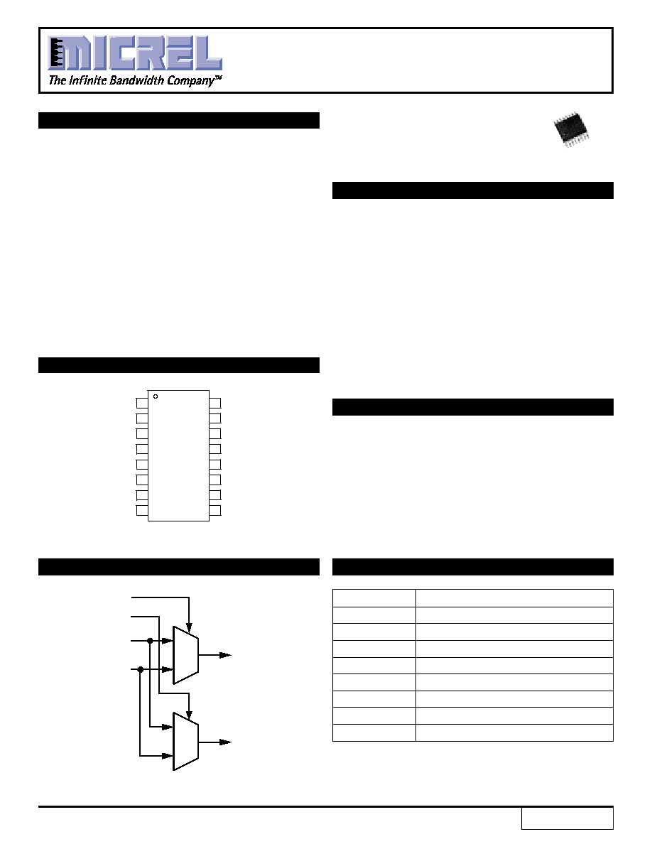
PIN CONFIGURATION
FUNCTIONAL BLOCK DIAGRAM
1
Rev.: B
Amendment: /0
Issue Date:
March 2003
PIN NAMES
Pin
Function
D0, /D0
CML/PECL/LVPECL Input Data
D1, /D1
CML/PECL/LVPECL Input Data
Q0, /Q0
CML Output Data
Q1, /Q1
CML Output Data
S0, /S0
CML/PECL/LVPECL Select Input
S1, /S1
CML/PECL/LVPECL Select Input
GND
Ground
V
CC
V
CC
SuperLite is a trademark of Micrel, Inc.
S
0
1
D0
D1
S0
Q0
S
0
1
Q1
S1
1
GND
D0
/D0
S0
/S0
/D1
D1
GND
16 VCC
Q0
/Q0
S1
/S1
/Q1
Q1
VCC
15
14
13
12
11
10
9
2
3
4
5
6
7
8
QSOP
16-Pin QSOP
SuperLiteTM
2
SuperLiteTM
SY55854U
Micrel
PIN DESCRIPTIONS
D0, /D0 ≠ CML/PECL/LVPECL Input (Differential)
This is one of the data inputs to the crosspoint. It will be
switched either to the Q0 output, the Q1 output, both
outputs, or neither output, depending on the state of the
S0 and S1 inputs.
D1, /D1 ≠ CML/PECL/LVPECL Input (Differential)
This is the other data input to the crosspoint. It will be
switched either to the Q0 output, the Q1 output, both
outputs, or neither output, depending on the state of the
S0 and S1 inputs.
Q0, /Q0 ≠ CML Output (Differential)
This is one output from the crosspoint. Input S0 selects
either the D0 or the D1 input to be switched to this
output.
Q1, /Q1 ≠ CML Output (Differential)
This is the other output from the crosspoint. Input S1
selects either the D0 or D1 input to be switched to this
output.
S0, /S0 ≠ CML/PECL/LVPECL Input (Differential)
This selects input chooses which data input switches to
the Q0 output. S0 logic low selects the D0 input, while
S0 logic high selects the B input.
S1, /S1 ≠ CML/PECL/LVPECL Input (Differential)
This select input chooses which data input switches to
the Q1 output. S1 logic low selects the D0 input, while
S1 logic high selects the D1 input.
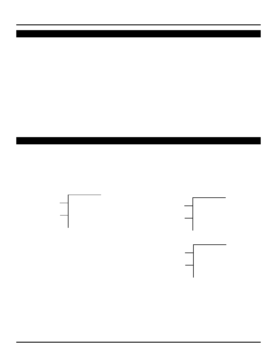
FUNCTIONAL DESCRIPTION
V
CC
NC
X
/X
Figure 1. Hard Wiring a Logic "1"
(1)
NC
NC
X
/X
V
CC
> 3.0V
NC
V
CC
X
/X
V
CC
3.0V
Figure 2. Hard Wiring a Logic "0"
(1)
Establishing Static Logic Inputs
The true pin of an input pair is internally biased to ground
through a 75k
resistor. The complement pin of an input
pair is internally biased halfway between V
CC
and ground
by a voltage divider consisting of two 75k
resistors. In this
way, unconnected inputs appear as logic zeros. To keep an
input at static logic zero at V
CC
> 3.0V, leave both inputs
unconnected. For V
CC
3.0V, connect the complement
input to V
CC
and leave the true input unconnected. To make
an input static logic one, connect the true input to V
CC
,
leave the complement input unconnected. These are the
only two safe ways to cause inputs to be at a static value.
In particular, no input pin should be directly connected to
ground. All NC (no connect) pins should be unconnected.
Note 1.
X is either D0, D1, S0, or S1 input. /X is either /D0, /D1, /S0, or
/S1 input.
Usage
SY55854U is very versatile. Tying its select inputs in
various ways varies its functionality. For example, tying the
select inputs together turns SY55854U into a redundant
distributor. Either input will be switched to both outputs
simultaneously. This is very useful in redundant backplane
applications. By cross-tying the select inputs, SY55854U
becomes a true crosspoint, selecting between "straight
through" and "cross connected" operation. Also, using the
select inputs independently, SY55854U functions as two
multiplexers. Setting the select inputs to static values turns
SY55854U into a dual buffer, or a fan-out buffer.
To make larger crosspoints, cascade SY55854U devices,
either in a tree or in a Banyan structure, as appropriate for
your application.
3
SuperLiteTM
SY55854U
Micrel
CML TERMINATION
100
100
100
100
SY55854U
v
cc
v
cc
100
50
50
8mA
Figure 3a.
Differentially Terminated
(50
Load CML Output)
100
100
100
50
SY55854U
v
cc
50
8mA
50
100
50
Figure 3b.
Individually Terminated
(50
Load CML Output)
All inputs accept the output from any other member of
this family. All outputs are source terminated 100
CML
differential drivers as shown in Figures 3 and 4. SY55854U
expects the inputs to be terminated, and that good high
speed design practices be adhered to. SY55854U inputs
are designed to accept a termination resistor between the
true and complement inputs of a differential pair. 0402 form
factor chip resistors will fit with some trace fanout.
100
100
200
SY55854U
V
CC
8mA
100
100
Figure 4.
100
Load CML Output
S0
S1
Q0
Q1
Function
0
0
D0
D0
Fan-Out Buffer
0
1
D0
D1
Dual Buffer
1
0
D1
D0
Dual Buffer
1
1
D1
D1
Fan-Out Buffer
CTL
CTL
Same
Same
Redundant Distribution
CTL
/CTL
Opposite
Opposite
Crosspoint
TRUTH TABLE
4
SuperLiteTM
SY55854U
Micrel
T
A
= ≠40
∞
C
T
A
= 0
∞
C
T
A
= +25
∞
C
T
A
= +85
∞
C
Symbol
Parameter
Min.
Max.
Min.
Max.
Min.
Max.
Min.
Max.
Unit
V
CC
Power Supply Voltage
2.3
5.7
2.3
5.7
2.3
5.7
2.3
5.7
V
I
CC
Power Supply Current
--
60
--
60
--
60
--
60
mA
Note 1.
Specification for packaged product only.
DC ELECTRICAL CHARACTERISTICS
(1)
V
CC
= 2.3V to 5.7V; GND = 0V
Symbol
Parameter
Min.
Typ.
Max.
Unit
Condition
V
ID
Differential Input Voltage
100
--
--
mV
V
IH
Input HIGH Voltage
1.6
--
V
CC
V
V
IL
Input LOW Voltage
1.5
--
V
CC
≠ 0.1
V
V
OH
Output HIGH Voltage
V
CC
≠ 0.020
V
CC
≠ 0.010
V
CC
V
No Load
V
OL
Output LOW Voltage
V
CC
≠ 0.97
V
CC
≠ 0.825
V
CC
≠ 0.660
V
No Load
V
OS
Output Voltage Swing
(3)
0.700
0.800
0.950
V
No Load
0.400
100
Environment
(5)
0.200
50
Environment
(4)
R
DRIVE
Output Source Impedance
80
100
120
CML DC ELECTRICAL CHARACTERISTICS
(1)
V
CC
= 2.3V to 5.7V; GND = 0V; T
A
= ≠40
∞
C to +85
∞
C
(2)
Note 1.
Specification for packaged product only.
Note 2.
Equilibrium temperature.
Note 3.
Actual voltage levels and differential swing will depend on customer termination scheme. Typically, a 400mV swing is available in the 100
environment and a 200mV swing in the 50
environment. Refer to the "CML Termination" diagram for more details.
Note 4.
See Figure 3a and 3b.
Note 5.
See Figure 4.
Symbol
Rating
Value
Unit
V
CC
Power Supply Voltage
≠0.5 to +6.0
V
V
I
Input Voltage
≠0.5 to V
CC
+0.5
V
V
O
CML Output Voltage
V
CC
≠1.0 to V
CC
+0.5
V
T
A
Operating Temperature Range
≠40 to +85
∞
C
T
store
Storage Temperature Range
≠65 to +150
∞
C
Note 1.
Permanent device damage may occur if ABSOLUTE MAXIMUM RATINGS are exceeded. This is a stress rating only and functional operation
is not implied at conditions other than those detailed in the operational sections of this data sheet. Exposure to ABSOLUTE MAXIMUM
RATlNG conditions for extended periods may affect device reliability.
ABSOLUTE MAXIMUM RATINGS
(1)
5
SuperLiteTM
SY55854U
Micrel
Symbol
Parameter
Min.
Typ.
Max.
Unit
Condition
f
MAX
Max. Operating Frequency
2.5
--
--
GHz
t
PLH
Propagation Delay,
--
--
400
ps
t
PHL
S0, S1, D0, D1 to Q0, Q1
t
SKEW
Within-Device Skew
(3)
--
--
15
ps
Part-to-Part Skew (Diff.)
--
--
100
t
r
CML Output Rise/Fall Times
--
--
150
ps
t
f
(20% to 80%)
AC ELECTRICAL CHARACTERISTICS
(1, 2)
V
CC
= 2.3V to 5.7V; GND = 0V; T
A
= ≠40
∞
C to +85
∞
C
Note 1.
Specification for packaged product only.
Note 2.
Tested using environment of Figure 3b, 50
load CML output.
Note 3.
Worst case difference between Q0 and Q1 from either A or B, when both outputs come from the same input
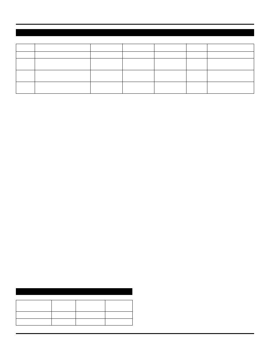
PRODUCT ORDERING CODE
Ordering
Package
Operating
Package
Code
Type
Range
Marking
SY55854UYI
Y16-1
Industrial
854U
SY55854UYITR
Y16-1
Industrial
854U