1
Precision Edge
Æ
SY58021U
Micrel, Inc.
M9999-062405
hbwhelp@micrel.com or (408) 955-1690
DESCRIPTION
Precision 1:4, LVPECL fanout buffer
Guaranteed AC performance over temperature/
voltage:
∑ >4GHz f
MAX
(clock)
∑ <100ps t
r
/ t
f
Times
∑ <300ps t
pd
∑ <15ps max skew
Low jitter performance
∑ <10ps
pp
total jitter (clock)
∑ <1ps
rms
random jitter (data)
∑ <10ps
pp
deterministic jitter (data)
Accepts an input signal as low as 100mV
Unique input termination and VT pin accepts
DC-coupled and AC-coupled differential inputs:
LVPECL, LVDS, and CML
100k LVPECL compatible 800mV swing output
Power supply 2.5V
±
5% and 3.3V
±
10%
≠40
∞
C to +85
∞
C temperature range
Available in 16-pin (3mm
◊◊
◊◊
◊
3mm) MLFTM package
FEATURES
4GHz, 1:4 LVPECL FANOUT
BUFFER/ TRANSLATOR
WITH INTERNAL TERMINATION
Precision Edge
Æ
SY58021U
APPLICATIONS
s All SONET and All GigE clock distribution
s
Fibre Channel clock and data distribution
s
Backplane distribution
s
High-end, low skew, multiprocessor synchronous
clock distribution
Rev.: D
Amendment: /0
Issue Date:
June 2005
The SY58021U is a 2.5V/3.3V precision, high-speed, fully
differential 1:4 LVPECL fanout buffer. Optimized to provide
four identical output copies with less than 15ps of skew and
less than 10ps
pp
total jitter, the SY58021U can process
clock signals as fast as 4GHz.
The differential input includes Micrel's unique, 3-pin input
termination architecture interfaces to differential LVPECL,
CML, and LVDS signals (AC- or DC-coupled) as small as
100mV without any level-shifting or termination resistor
networks in the signal path. For AC-coupled input interface
applications, an on-board output reference voltage (V
REF-
AC
) is provided to bias the VT pin. The outputs are 100k
LVPECL compatible, with extremely fast rise/fall times
guaranteed to be less than 100ps.
The SY58021U operates from a 2.5V
±
5% supply or
3.3V
±
10% supply and is guaranteed over the full industrial
temperature range (≠40
∞
C to +85
∞
C). For applications that
require faster rise/fall times, or greater bandwidth, consider
the SY58022U 1:4 fanout buffer with 400mV LVPECL output
swing, or the SY58020U 1:4 CML fanout buffer. The
SY58021U is part of Micrel's high-speed, Precision Edge
Æ
product line.
All support documentation can be found on Micrel's web
site at www.micrel.com.
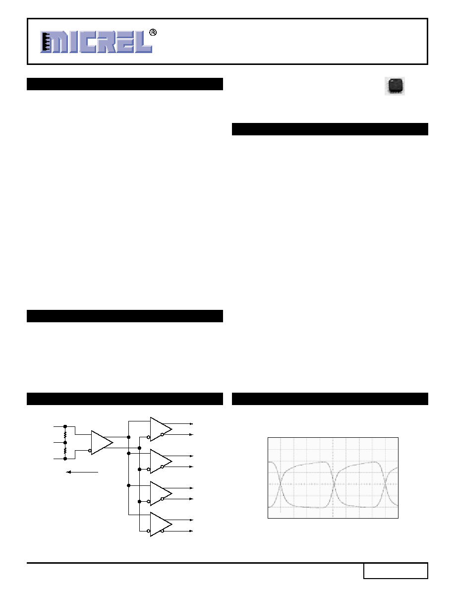
FUNCTIONAL BLOCK DIAGRAM
TYPICAL PERFORMANCE
Precision Edge is a registered trademark of Micrel , Inc.
MicroLeadFrame and MLF are trademarks of Amkor Technology, Inc.
IN
/IN
Q1
/Q1
Q0
/Q0
V
T
50
50
V
REF-AC
Q3
/Q3
Q2
/Q2
Precision Edge
Æ
1.25GHz Output
TIME (100ps/div.)
Amplitude (200mV/div
.)
2
Precision Edge
Æ
SY58021U
Micrel, Inc.
M9999-062405
hbwhelp@micrel.com or (408) 955-1690
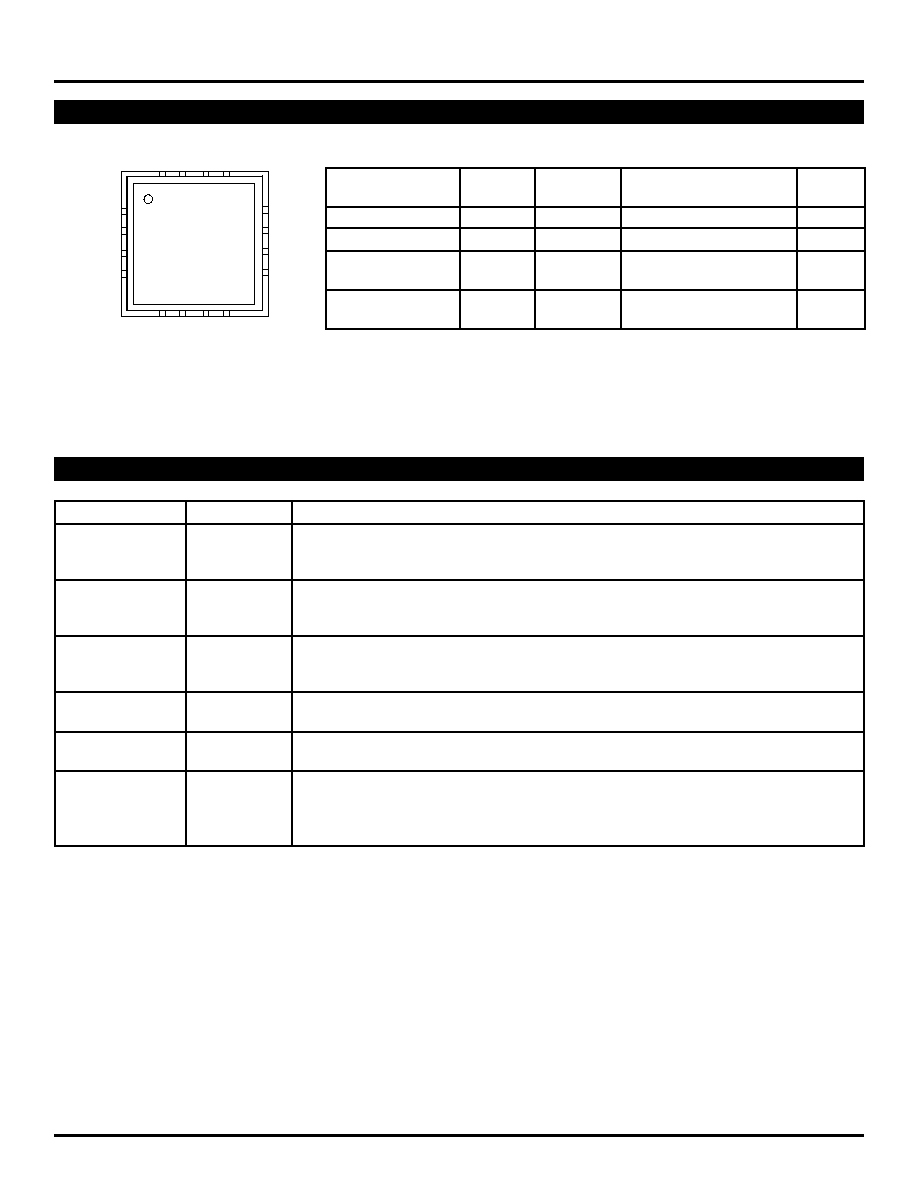
PACKAGE/ORDERING INFORMATION
Pin Number
Pin Name
Pin Function
1, 4
IN, /IN
Differential Input: This input pair receives the signal to be buffered. Each pin of this pair
internally terminates with 50
to the VT pin. Note that this input will default to an
indeterminate state if left open. See "Input Interface Applications" section.
2
VT
Input Termination Center-Tap: Each input terminates to this pin. The V
T
pin provides a
center-tap for each input (IN, /IN) to the termination network for maximum interface
flexibility. See "Input Interface Applications" section.
3
VREF-AC
Reference Output Voltage: This output biases to V
CC
≠1.2V. It is used when AC-coupling
to differential inputs. Connect V
REF-AC
directly to the VT pin. Bypass with 0.01
µ
F low ESR
capacitor to V
CC
. See "Input Interface Applications" section.
8, 13
VCC
Positive Power Supply: Bypass with 0.1
µ
F//0.01
µ
F low ESR capacitors as close to the
V
CC
pins as possible.
5, 16
GND,
Ground. Exposed pad must be connected to a ground plane that is the same potential as
Exposed Pad
the ground pin.
14, 15
/Q0, Q0,
LVPECL Differential Output Pairs: Differential buffered output copy of the input signal. The
11, 12
/Q1, Q1,
output swing is typically 800mV Proper termination is 50
to V
CC
≠2V at the receiving end.
9, 10
/Q2, Q2,
Unused output pairs may be left floating with no impact on jitter or skew.
6, 7
/Q3, Q3
See "LVPECL Output Termination" section.
PIN DESCRIPTION
13
14
15
16
12
11
10
9
1
2
3
4
8
7
6
5
IN
VT
VREF-AC
/IN
Q1
/Q1
Q2
/Q2
GND
Q0
/Q0
VCC
GND
/Q3
Q3
VCC
16-Pin MLFTM (MLF-16)
Ordering Information
(1)
Package
Operating
Package
Lead
Part Number
Type
Range
Marking
Finish
SY58021UMI
MLF-16
Industrial
021U
Sn-Pb
SY58021UMITR
(2)
MLF-16
Industrial
021U
Sn-Pb
SY58021UMG
MLF-16
Industrial
021U with
Pb-Free
Pb-Free bar-line indicator
NiPdAu
SY58021UMGTR
(2)
MLF-16
Industrial
021U with
Pb-Free
Pb-Free bar-line indicator
NiPdAu
Notes:
1. Contact factory for die availability. Dice are guaranteed at T
A
= 25
∞
C, DC electricals only.
2. Tape and Reel.
3
Precision Edge
Æ
SY58021U
Micrel, Inc.
M9999-062405
hbwhelp@micrel.com or (408) 955-1690
Absolute Maximum Ratings
(1)
Power Supply Voltage (V
CC
) ...................... ≠0.5V to +4.0V
Input Voltage (V
IN
) ......................................... ≠0.5V to V
CC
LVPECL Output Current (I
OUT
)
Continuous ............................................................. 50mA
Surge .................................................................... 100mA
Source or sink current on VT pin
V
T
Current ..........................................................
±
100mA
Source or sink current on IN, /IN
Input Current ........................................................
±
50mA
Source or sink current on V
REF-AC
(4)
V
REF
Current .......................................................
±
1.5mA
Soldering, (20 seconds) ............................................ 260
∞
C
Storage Temperature Range (T
S
) ............ ≠65
∞
C to +150
∞
C
Operating Ratings
(2)
Power Supply Voltage (V
CC
) ................. +2.375V to +3.60V
Operating Temperature Range (T
A
) ........... ≠40
∞
C to +85
∞
C
Package Thermal Resistance
MLFTM (
JA
)
Still-Air ............................................................. 60
∞
C/W
500 lpfm ........................................................... 54
∞
C/W
MLFTM (
JB
)
Junction-to-Board Resistance
(3)
...................... 33
∞
C/W
T
A
= ≠40
∞
C to 85
∞
C
Symbol
Parameter
Condition
Min
Typ
Max
Units
V
CC
Power Supply Voltage
V
CC
= 2.5V
2.375
2.5
2.625
V
V
CC
= 3.3V
3.0
3.3
3.60
V
I
CC
Power Supply Current
No load, V
CC
= max.
125
160
mA
V
IH
Input HIGH Voltage
IN, /IN, Note 6
V
CC
≠1.6
V
CC
V
V
IL
Input LOW Voltage
IN, /IN
0
V
IH
≠0.1
V
V
IN
Input Voltage Swing
IN, /IN; see Figure 1a.
0.1
1.7
V
V
DIFF_IN
Differential Input Voltage Swing
IN, /IN; see Figure 1b.
0.2
3.4
V
R
IN
IN-to-V
T
Resistance
40
50
60
V
T IN
IN-to-V
T
Voltage
1.28
V
V
REF-AC
Output Reference Voltage
V
CC
≠1.30 V
CC
≠1.2
V
CC
≠1.1
V
INPUT DC ELECTRICAL CHARACTERISTICS
(5)
V
CC
= 3.3V
±
10% or 2.5
±
5%; R
L
= 50
to V
CC
≠2V; T
A
= ≠40
∞
C to 85
∞
C, unless otherwise stated.
Symbol
Parameter
Condition
Min
Typ
Max
Units
V
OH
Output HIGH Voltage
V
CC
≠1.145
V
CC
≠0.895
V
V
OL
Output LOW Voltage
V
CC
≠1.945
V
CC
≠1.695
V
V
OUT
Output Voltage Differential Swing
see Figure 1a.
550
780
1050
mV
V
DIFF_OUT
Differential Output Voltage Swing
see Figure 1b.
1100
1560
2100
mV
Notes:
1. Permanent device damage may occur if ratings in the "Absolute Maximum Ratings" section are exceeded. This is a stress rating only and functional
operation is not implied for conditions other than those detailed in the operational sections of this data sheet. Exposure to absolute maximum ratings
conditions for extended periods may affect device reliability.
2. The data sheet limits are not guaranteed if the device is operated beyond the operating ratings.
3. Thermal performance assumes exposed pad is soldered (or equivalent) to the device's most negative potential on the PCB.
4. Due to the limited drive capability, use for input of the same package only.
5. The circuit is designed to meet the DC specifications shown in the above table after thermal equilibrium has been established.
6. V
IH
(min.) not lower than 1.2V.
LVPECL OUTPUT DC ELECTRICAL CHARACTERISTICS
(5)
4
Precision Edge
Æ
SY58021U
Micrel, Inc.
M9999-062405
hbwhelp@micrel.com or (408) 955-1690
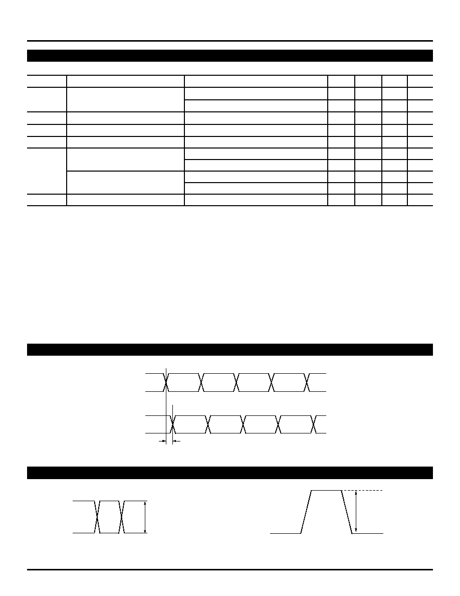
TIMING DIAGRAM
/IN
IN
/Q
Q
t
pd
SINGLE-ENDED AND DIFFERENTIAL SWINGS
V
IN
,
V
OUT
800mV
Figure 1a. Single-Ended Voltage Swing
V
DIFF_IN
,
V
DIFF_OUT
1.6V
Figure 1b. Differential Voltage Swing
V
CC
= 2.5V
±
5% or 3.3V
±
10%; R
L
= 50
to V
CC
≠2V; T
A
= ≠40
∞
C to +85
∞
C, unless otherwise stated.
Symbol
Parameter
Condition
Min
Typ
Max
Units
f
MAX
Maximum Operating Frequency
V
OUT
400mV
Clock
4
GHz
NRZ Data
5
Gbps
t
pd
Propagation Delay
150
220
300
ps
t
CHAN
Channel-to-Channel Skew
Note 7
4
15
ps
t
SKEW
Part-to-Part Skew
Note 8
50
ps
t
JITTER
Clock
Cycle-to-Cycle Jitter
Note 9
1
ps
RMS
Total Jitter
Note 10
10
ps
PP
Data
Random Jitter
Note 11
2.5Gbps ≠ 3.2Gbps
1
ps
RMS
Deterministic Jitter
Note 12
2.5Gbps ≠ 3.2Gbps
10
ps
PP
t
r
, t
f
Output Rise/Fall Time 20% to 80%
At full swing.
35
75
110
ps
Notes:
7.
Skew is measured between outputs of the same bank under identical transitions.
8.
Skew is defined for two parts with identical power supply voltages at the same temperature and with no skew of the edges at the respective inputs.
9.
Cycle-to-cycle jitter definition: the variation of periods between adjacent cycles, T
n
≠T
n≠1
where T is the time between rising edges of the output
signal.
10. Total jitter definition: with an ideal clock input of frequency
f
MAX
, no more than one output edge in 10
12
output edges will deviate by more than the
specified peak-to-peak jitter value.
11. Random jitter is measured with a K28.7 comma detect character pattern, measured at 2.5Gbps/3.2Gbps.
12. Deterministic jitter is measured at 2.5Gbps/3.2Gbps with both K28.5 and 2
23
≠1 PRBS pattern
AC ELECTRICAL CHARACTERISTICS
5
Precision Edge
Æ
SY58021U
Micrel, Inc.
M9999-062405
hbwhelp@micrel.com or (408) 955-1690
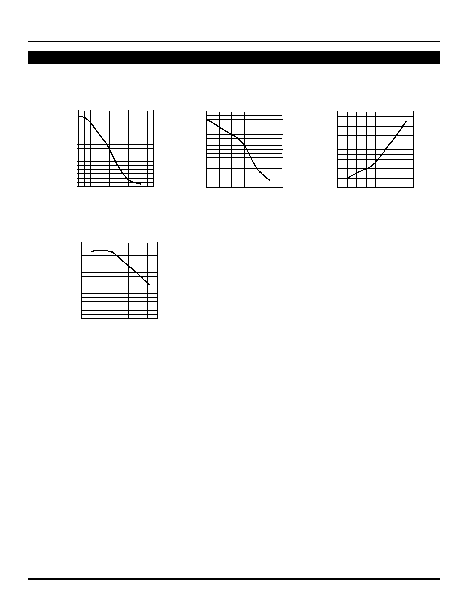
TYPCIAL OPERATING CHARACTERISTICS
V
CC
= 2.5V, GND = 0, V
IN
= 100mV, T
A
= 25
∞
C, unless otherwise stated.
0
100
200
300
400
500
600
700
800
900
0
2000
4000
6000
8000
10000
12000
AMPLITUDE (mV)
FREQUENCY (MHz)
Amplitude
vs. Frequency
174
176
178
180
182
184
186
188
190
192
194
0
200 400 600 800 1000 1200
PROPAGATION DELAY (ps)
INPUT VOLTAGE SWING (mV)
Propagation Delay vs.
Input Voltage Swing
176
177
178
179
180
181
182
183
184
-60 -40 -20 0
20 40 60 80 100
PROPAGATION DELAY (ps)
TEMPERATURE (
∞
C)
Propagation Delay vs.
Temperature
0
0.5
1.0
1.5
2.0
2.5
3.0
3.5
4.0
4.5
-60 -40 -20 0
20 40 60 80 100
SKEW (ps)
TEMPERATURE (
∞
C)
Skew
vs. Temperature