
SY58609U
4.25Gbps Precision, CML 2:1 MUX with
Internal Termination and Fail Safe Input
Precision Edge is a registered trademark of Micrel, Inc.
MLF and
Micro
LeadFrame are registered trademarks of Amkor Technology.
Micrel Inc. ∑ 2180 Fortune Drive ∑ San Jose, CA 95131 ∑ USA ∑ tel +1 (408) 944-0800 ∑ fax + 1 (408) 474-1000 ∑ http://www.micrel.com
October 2006
M9999-103106-A
hbwhelp@micrel.com
or (408) 955-1690
General Description
The SY58609U is a 2.5/3.3V, high-speed, fully
differential CML 2:1 MUX capable of processing clock
signals up to 2.5GHz and data patterns up to 4.25Gbps.
The SY58609U is optimized to provide a buffered output
of the selected input with less than 20ps of skew and
less than 10ps
pp
total jitter.
The differential input includes Micrel's unique, 3-pin
input termination architecture that interfaces to LVPECL,
LVDS or CML differential signals, (AC- or DC-coupled)
as small as 100mV (200mV
pp
) without any level-shifting
or termination resistor networks in the signal path. For
AC-coupled input interface applications, an integrated
reference voltage (V
REF-AC
) is provided to bias the V
T
pin.
The outputs are 400mV CML, with extremely fast
rise/fall times guaranteed to be less than 90ps.
The SY58609U operates from a 2.5V ±5% supply or
3.3V ±10% supply and is guaranteed over the full
industrial temperature range (≠40∞C to +85∞C). For
applications that require LVPECL or LVDS outputs,
consider Micrel's SY58610U and SY58611U, 2:1 MUX
with 800mV and 325mV output swings, respectively.
The SY58609U is part of Micrel's high-speed, Precision
Edge
Æ
product line.
Datasheets and support documentation can be found on
Micrel's web site at:
www.micrel.com
.
Functional Block Diagram
Precision Edge
Æ
Features
∑ Precision 400mV CML 2:1 MUX
∑ Guaranteed AC performance over temperature and
voltage:
≠ DC-to > 4.25Gbps throughput
≠ <370ps propagation delay (IN-to-Q)
≠ <90ps
rise/fall
times
∑ Fail Safe Input
≠ Prevents outputs from oscillating when input is
invalid
∑ Ultra-low jitter design
≠ <1ps
RMS
cycle-to-cycle jitter
≠ <10ps
PP
total jitter
≠ <1ps
RMS
random jitter
≠ <10ps
PP
deterministic jitter
∑ High-speed CML outputs
∑ 2.5V ±5% or 3.3V ±10% power supply operation
∑ Industrial temperature range: ≠40∞C to +85∞C
∑ Available in 16-pin (3mm x 3mm) MLF
Æ
package
Applications
∑ Data Distribution: OC-48, OC-48+FEC, XAUI
∑ SONET clock and data distribution
∑ Fibre Channel clock and data distribution
∑ Gigabit Ethernet clock and data distribution
Markets
∑ Storage
∑ ATE
∑ Test and measurement
∑ Enterprise networking equipment
∑ High-end servers
∑ Access
Micrel, Inc.
SY58609U
October 2006
2
M9999-103106-A
hbwhelp@micrel.com
or (408) 955-1690
Ordering Information
(1)
Part Number
Package
Type
Operating
Range
Package Marking
Lead Finish
SY58609UMG MLF-16
Industrial
609U with Pb-Free
bar-line indicator
NiPdAu
Pb-Free
SY58609UMGTR
(2)
MLF-16 Industrial
609U with Pb-Free
bar-line indicator
NiPdAu
Pb-Free
Notes:
1. Contact factory for die availability. Dice are guaranteed at T
A
= 25∞C, DC Electricals only.
2. Tape
and
Reel.
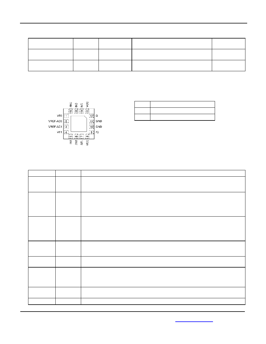
Pin Configuration
16-Pin MLF
Æ
Truth Table
SEL Output
0 IN0
Selected
1 IN1
Selected
Pin Description
Pin Number
Pin Name
Pin Function
1, 4
VT0, VT1
Input Termination Center-Tap: Each side of the differential input pair terminates to the VT
pin. This pin provides a center-tap to a termination network for maximum interface flexibility.
See "Input Interface Applications" subsection.
2, 3
VREF-AC0,
VREF-AC1
Reference Voltage: These outputs bias to V
CC
≠1.2V. They are used for AC-coupling inputs
IN and /IN. Connect VREF-AC directly to the corresponding VT pin. Bypass with 0.01µF low
ESR capacitor to VCC. Due to limited drive capability, the VREF-AC pin is only intended to
drive its respective VT pin. Maximum sink/source current is ±0.5mA. See "Input Interface
Applications" subsection.
5, 6
15, 16
IN1, /IN1
IN0, /IN0
Differential Inputs: These input pairs are the differential signal inputs to the device. Inputs
accept DC-Coupled differential signals as small as 100mV
(200mVpp). Each pin of the pairs
internally terminates with 50 to the VT pin. If the input swing falls below a certain
threshold (typical 30mV), the Fail Safe Input (FSI) feature will guarantee a stable output by
latching the output to its last valid state. See "Input Interface Applications" subsection.
7 SEL
Single-Ended Input: This single-ended TTL/CMOS-compatible input selects the inputs to the
multiplexer. Note that this input is internally connected to a 25k pull-up resistor and will
default to logic HIGH state if left open. The input-switching threshold is V
CC
/2.
8, 13
VCC
Positive Power Supply: Bypass with 0.1uF//0.01uF low ESR capacitors as close to the V
CC
pins as possible.
9, 12
/Q, Q
CML Differential Output Pair: Differential buffered output copy of the selected input signal.
The output swing is typically 400mV. Normally terminate with 100 across Q and /Q.
Unused output pair may be left floating with no impact on jitter. See "CML Output
Termination" subsection.
10, 11
GND
Ground. Exposed pad must be connected to a ground plane that is the same potential as
the ground pins.
14 NC
No
connect.

Micrel, Inc.
SY58609U
October 2006
3
M9999-103106-A
hbwhelp@micrel.com
or (408) 955-1690
Absolute Maximum Ratings
(1)
Supply Voltage (V
CC
) ............................... ≠0.5V to +4.0V
Input Voltage (V
IN
) .......................................≠0.5V to V
CC
CML Output Voltage (V
OUT
).......... V
CC
-1.0V to V
CC
+0.5V
Current (V
T
)
Source or sink on VT pin .............................±100mA
Input Current
Source or sink Current on (IN, /IN) ................±50mA
Current (V
REF
)
Source or sink current on V
REF
-AC
(4)
............±0.5mA
Maximum operating Junction Temperature ......... 125∞C
Lead Temperature (soldering, 20sec.) .................. 260∞C
Storage Temperature (T
s
) ....................≠65∞C to +150∞C
Operating Ratings
(2)
Supply Voltage (V
CC
)....................... +2.375V to +3.60V
Ambient Temperature (T
A
) ................... ≠40∞C to +85∞C
Package Thermal Resistance
(3)
MLF
Æ
Still-air (
JA
)........................................... 60∞C/W
Junction-to-board (
JB
) ......................... 33∞C/W
DC Electrical Characteristics
(5)
T
A
= ≠40∞C to +85∞C, unless otherwise stated.
Symbol Parameter
Condition
Min Typ Max Units
V
CC
Power Supply Voltage Range
2.375
3.0
2.5
3.3
2.625
3.6
V
I
CC
Power Supply Current
No load, max. V
CC
50
60
mA
R
DIFF_IN
Differential Input Resistance
(IN-to-/IN)
90 100
110
V
IH
Input HIGH Voltage
(IN, /IN)
IN, /IN
1.2
V
CC
V
V
IL
Input LOW Voltage
(IN, /IN)
IN, /IN
0.2
V
IH
≠0.1 V
V
IN
Input Voltage Swing
(IN, /IN)
see Figure 3a, Note 6
0.1 1.0
V
V
DIFF_IN
Differential Input Voltage Swing
(|IN - /IN|)
see Figure 3b
0.2 V
V
IN_FSI
Input Voltage Threshold that
Triggers FSI
30
100
mV
V
REF-AC
AC
Reference
Voltage
V
CC
-1.3 V
CC
-1.0 V
V
T_IN
Voltage from Input to V
T
1.28
V
Notes:
1. Permanent device damage may occur if absolute maximum ratings are exceeded. This is a stress rating only and functional operation is not
implied at conditions other than those detailed in the operational sections of this data sheet. Exposure to absolute maximum ratings conditions for
extended periods may affect device reliability.
2. The data sheet limits are not guaranteed if the device is operated beyond the operating ratings.
3. Package thermal resistance assumes exposed pad is soldered (or equivalent) to the device's most negative potential on the PCB.
JB
and
JA
values are determined for a 4-layer board in still-air number, unless otherwise stated.
4. Due to the limited drive capability, use for input of the same package only.
5. The circuit is designed to meet the DC specifications shown in the above table after thermal equilibrium has been established.
6. V
IN
(max) is specified when V
T
is floating.

Micrel, Inc.
SY58609U
October 2006
4
M9999-103106-A
hbwhelp@micrel.com
or (408) 955-1690
CML Outputs DC Electrical Characteristics
(7)
V
CC
= +2.5V ±5% or +3.3V ±10%, R
L
= 100 across the outputs; T
A
= ≠40∞C to +85∞C, unless otherwise stated.
Symbol Parameter
Condition
Min
Typ
Max Units
V
OH
Output HIGH Voltage
R
L
= 50 to V
CC
V
CC
-0.020 V
CC
-0.010 V
CC
V
V
OUT
Output Voltage Swing
See Figure 3a
325
400
mV
V
DIFF_OUT
Differential Output Voltage Swing
See Figure 3b
650 800
mV
R
OUT
Output
Source
Impedance
45
50 55
LVTTL/CMOS DC Electrical Characteristics
(7)
V
CC
= 2.5V ±5% or 3.3V ±10%; T
A
= ≠40∞C to + 85∞C, unless otherwise stated.
Symbol Parameter
Condition
Min
Typ
Max Units
V
IH
Input HIGH Voltage
2.0
V
V
IL
Input LOW Voltage
0.8
V
I
IH
Input HIGH Current
-125
30
µA
I
IL
Input LOW Current
-300
µA
Notes:
7. The circuit is designed to meet the DC specifications shown in the above table after thermal equilibrium has been established.

Micrel, Inc.
SY58609U
October 2006
5
M9999-103106-A
hbwhelp@micrel.com
or (408) 955-1690
AC Electrical Characteristics
(8)
V
CC
= +2.5V ±5% or +3.3V ±10%, R
L
= 100 across the outputs; Input t
R
/t
F
< 300ps, T
A
= ≠40∞C to +85∞C, unless
otherwise stated.
Symbol Parameter
Condition
Min Typ Max Units
NRZ Data
4.25
Gbps
f
MAX
Maximum
Frequency
V
OUT
> 200mV Clock
2.5
3
GHz
V
IN
:
100mV-200mV
180 330 450 ps
Propagation Delay IN-to-Q
V
IN
:
>200mV
140 270 370 ps
t
PD
SEL-to-Q
150
450
ps
Input-to-Input Skew
Note 9, 10
5
20
ps
t
Skew
Part-to-Part Skew
Note 11
150
ps
Data Random Jitter
Note 12
1
ps
RMS
Deterministic Jitter
Note 13
10
ps
PP
Clock Cycle-to-Cycle Jitter Note 14
1
ps
RMS
t
Jitter
Total Jitter
Note 15
10
ps
PP
t
R
,t
F
Output Rise/Fall Times
(20% to 80%)
At full output swing.
35
50
90
ps
Duty Cycle
Differential I/O
47
53
%
Notes:
8.
High-frequency AC-parameters are guaranteed by design and characterization.
9.
Input-to-Input skew is the time difference between the two inputs and one output, under identical input transitions.
9.
Input-to-Input Skew is included in IN-to-Q propagation delay.
11. Part-to-part skew is defined for two parts with identical power supply voltages at the same temperature, same transition edge, and no skew at
the edges at the respective inputs.
12. Random jitter is measured with a K28.7 pattern, measured at f
MAX
.
13. Deterministic jitter is measured at 2.5Gbps with both K28.5 and 2
23
≠1 PRBS pattern.
14. Cycle-to-cycle jitter definition: the variation period between adjacent cycles over a random sample of adjacent cycle pairs. t
JITTER
_
CC
= T
n
≠T
n+1
,
where T is the time between rising edges of the output signal.
15. Total jitter definition: with an ideal clock input frequency of f
MAX
(device), no more than one output edge in 10^12 output edges will deviate by
more than the specified peak-to-peak jitter value.